

Fairchild Semiconductor DM74ALS640AWMX, DM74ALS640AWM, DM74ALS640AN Datasheet
© 2000 Fairchild Semiconductor Corporation DS008640 www.fairchildsemi.com
August 1985
Revised February 2000
DM74ALS640A Inverting Octal Bus Transceiver
DM74ALS640A
Inverting Octal Bus Transceiver
General Description
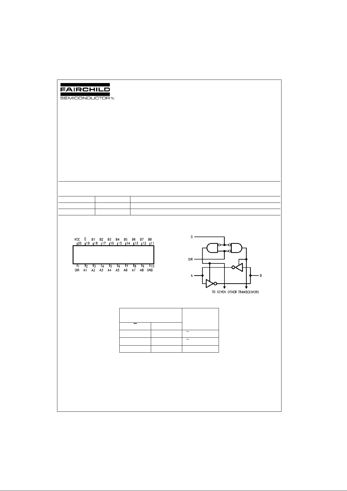
This inverting octal bus transce iver is designed for asynchronous two-way communica tion between data busses.
This device transmits data from the A b us to the B b us or
from the B bus to the A bus depending upon the level at the
direction control (DI R) input. The enable inp ut (G) can be
used to disable the device so the busses are effectively
isolated.
Features
■ Advanced Oxide-isolated Ion-implanted Schottky TTL
process
■ Switching performan ce is gu aranteed over full tempe rature and V
CC
supply range
■ Switching performance specified at 50 pF
■ PNP input design reduces input loading
Ordering Code:
Devices also availab le in Tape and Reel. Specify by appending th e s uffix let t er “X” to the ordering code.
Connection Diagram Logic Diagram
Function Table
L = LOW Logic Level
H = HIGH Logic Level
X = Either LOW or HIG H Logic Level
Order Number Package Number Package Description
DM74ALS640AWM M20B 20-Lead Small Outline Integrated Circuit (SOIC), JEDEC MS-013, 0.300 Wide
DM74ALS640AN N20A 20-Lead Plastic Dual-In-Line Package (PDIP), JEDEC MS-001, 0.300 Wide
Control
Inputs Operation
G
DIR
LLB
Data to A Bus
LHA
Data to B Bus
HXIsolation
www.fairchildsemi.com 2
DM74ALS640A
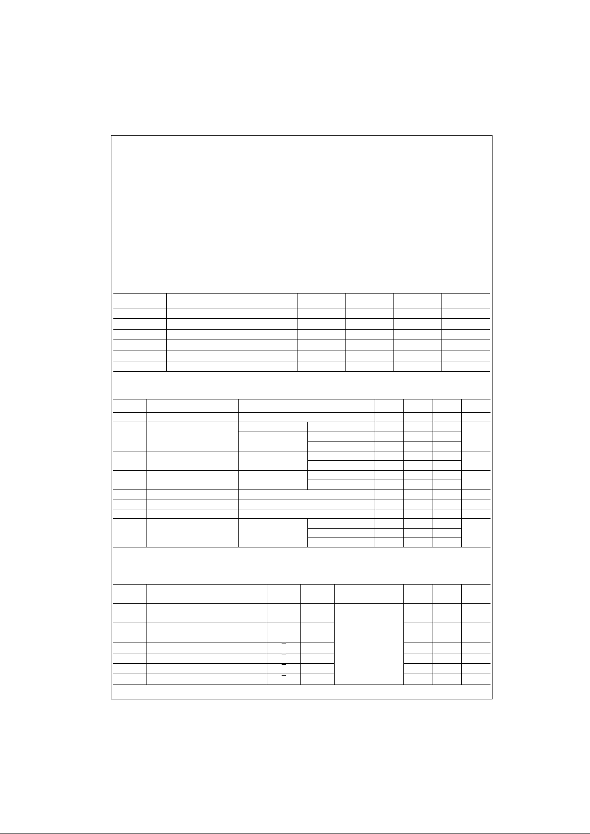
Absolute Maximum Ratings(Note 1)
Note 1: The “Absolute Maximum Ratin gs” are those v alues beyon d which
the safety of the dev ice cannot be guaranteed. T he device sh ould not be
operated at these limits. The parametric values defined in the Electrical
Characteristics tables are not guaranteed at the absolute maximum ratings.
The “Recommend ed O peratin g Cond itions” t able w ill defin e the co ndition s
for actual device operation.
Recommended Operating Conditions
Electrical Characteristics
Over Recommended Free Air Temperature Range
Note 2: For I/O ports, IIH and IILparameters includ e t he 3-STATE output current (I
OZL
and I
OZH
).
Switching Characteristics
Over Recommended Operating Free Air Temperature Range
Supply Voltage 7V
Input Voltage
Control Inputs 7V
I/O ports 5.5V
Operating Free Air Temperature Range 0°C to +70°C
Storage Temperature Range −65°C to +150°C
Typical θ
JA
N Package 53.0°C/W
M Package 72.0°C/W
Symbol Parameter Min Typ Max Units
V
CC
Supply Voltage 4.5 5 5.5 V
V
IH
HIGH Level Input Voltage 2 V
V
IL
LOW Level Input Voltage 0.8 V
I
OH
HIGH Level Output Current −15 mA
I
OL
LOW Level Output Current 24 mA
T
A
Operating Free Air Temperature Range 0 70 °C
Symbol Parameter Test Conditions Min Typ Max Units
V
IC
Input Clamp Voltage VCC = Min, II = −18 mA −1.5 V
V
OH
HIGH Level VCC = 4.5 to 5.5V IOH = −0.4 mA VCC − 2
Output Voltage VCC = Min IOH = − 3 mA 2.4 2.9 V
IOH = Max 2
V
OL
LOW Level VCC = Min IOL = 12 mA 0.25 0.4
V
Output Voltage IOL = 24 mA 0.35 0.5
I
I
Input Current at Maximum VCC = Max. I/O Ports, VI = 5.5V 100
µA
Input Voltage Control Inputs, VI = 7V 100
I
IH
HIGH Level Input Current VCC = Max, VI = 2.7V (Note 2) 20 µA
I
IL
LOW Level Input Current VCC = Max, VI = 0.4V (Note 2) −100 µA
I
O
Output Drive Current VCC = Max, VO = 2.25V −30 −112 mA
I
CC
Supply Current VCC = Max Outputs HIGH 19 45
Outputs LOW 23 55 mA
Outputs Disabled 17 50
Symbol Parameter
From To
Conditions Min Max Units
(Input) (Output)
t
PLH
Propagation Delay Time
A or B B or A
VCC = 4.5 to 5.5V,
111ns
LOW-to-HIGH Level Output CL = 50 pF,
t
PHL
Propagation Delay Time
A or B B or A
R1 = R2 = 500Ω
110ns
HIGH-to-LOW Level Output
t
PZH
Output Enable Time to HIGH Level Output G A or B 4 21 ns
t
PZL
Output Enable Time to LOW Level Output G A or B 5 24 ns
t
PHZ
Output Disable Time from HIGH Level Output G A or B 1 10 ns
t
PLZ
Output Disable Time from LOW Level Output G A or B 3 15 ns
 Loading...