

Fairchild Semiconductor DM74ALS573BSJ Datasheet
April 1984
Revised February 2000
DM74ALS573B
Extended Temperature Octal D-Type Transparent Latch
with 3-STATE Outputs
DM74ALS573B Extended Temperature Octal D-Type Transparent Latch with 3-STATE Outputs
General Description
These 8-bit register s feature totem-pole 3- STATE outputs
designed specifically fo r driving highly-capacitive or relatively low-impedance loa ds. Th e hi gh -im ped ance state and
increased high-logic-level drive provide these registers with
the capability of being connected directly to and driving the
bus lines in a bu s-or ga nized system without need fo r inte rface or pull-up components. They are particularly attractive
for implementing buffer registers, I/O ports, bidirectional
bus drivers, and working registers.
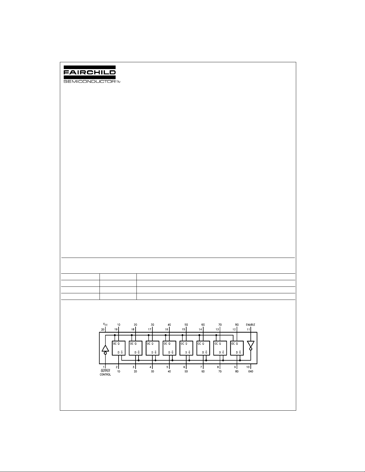
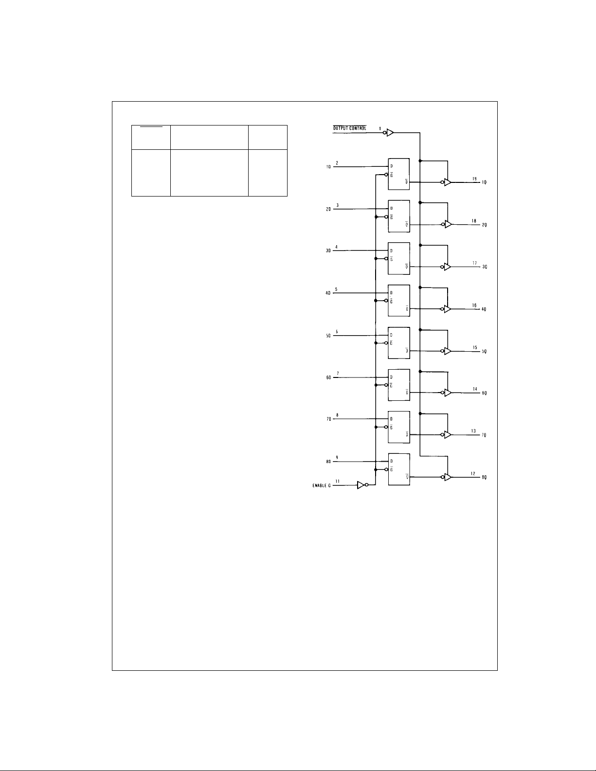
The eight latches of the DM74 AL S573 B are tran spa ren t Dtype latches. While the enable (G) is HIGH the Q outputs
will follow the data (D) inputs. When the enable is taken
LOW the output will be latched at the level of the data that
was set UP.
A buffered output control in put can be used to place the
eight outputs in either a normal logic state (HIGH or LOW
logic levels) or a high-impedance state. In the high-impedance state the outputs ne ither load nor dr ive the bus lines
significantly.
The output control does not affect th e internal oper ation of
the latches. That is, the old da ta can be retained or new
data can be entered even while the outputs are OFF.
Features
■ Switching specifications at 50 pF
■ Switching specifications guaranteed over full tempera-
ture and V
■ Advanced oxide-isolated, ion-implanted Schottky TTL
process
■ Functionally equivalent with DM74LS373
■ Improved AC perfo rma nce over DM74LS373 at a pp roxi -
mately half the power
■ 3-STATE buffer-type outputs dr ive bus lines d irectly
CC
range
Ordering Code:
Order Number Package Number Package Description
DM74ALS573BWM M20B 20-Lead Small Outline Integrated Circuit (SOIC), JEDEC MS-013, 0.300 Wide
DM74ALS573BSJ M20D 20-Lead Small Outline Package (SOP), EIAJ TYPE II, 5.3mm Wide
DM74ALS573BN N20A 20-Lead Plastic Dual-In-Line Package (PDIP), JEDEC MS-001, 0.300 Wide
Devices also availab le in Tape and Reel. Specify by appending th e s uffix let t er “X” to the ordering cod e.
Connection Diagram
© 2000 Fairchild Semiconductor Corporation DS006226 www.fairchildsemi.com
Function Table
Output Enable D Output
Control G Q
LHHH
DM74ALS573B
L = LOW State
H = HIGH State
X = Don’t Care
Z = High Impedance State
Q
LHLL
LLXQ
HXXZ
= Previous Condit ion of Q
0
Logic Diagram
0
www.fairchildsemi.com 2
Absolute Maximum Ratings(Note 1)
Supply Voltage 7V
Input Voltage 7V
Voltage Applied to Disabled Output 5.5V
OperatingFree Air Temperature Range 0°C to +70°C
Storage Temperature Range −65°C to +150°C
Typical θ
JA
N Package 56.0°C/W
Note 1: The “Absolute M aximu m R atin gs” are t hose valu es b eyo nd w hich
the safety of the device cannot be guaranteed. The device should not be
operated at these limits. The parametric values defined in the Electrical
Characteristics tables are not guaranteed at the absolute maximum ratings.
The “Recommend ed O peratin g Cond itions” t able w ill defin e the condit ions
for actual device operation.
M Package 75.0°C/W
Recommended Operating Conditions
Symbol Parameter Min Nom Max Units
V
CC
V
IH
V
IL
I
OH
I
OL
t
W
t
SU
t
H
T
A
Note 2: The (↓) arrow in dic ates the negative edg e of the enable is used for ref erence.
Supply Voltage 4.5 5 5.5 V
HIGH Level Input Voltage 2 V
LOW Level Input Voltage 0.8 V
HIGH Level Output Current −2.6 mA
LOW Level Output Current 24 mA
Width of Enable Pulse, HIGH 10 ns
Data Setup Time (Note 2) 10↓ ns
Data Hold Time (Note 2) 7↓ ns
Free Air Operating Temperature 0 70 °C
Electrical Characteristics
over recommended operating free air temperature range. All typical values are measured at VCC = 5V, TA = 25°C.
Symbol Parameter Conditions Min Typ Max Units
V
V
V
I
I
I
I
I
I
I
IK
OH
OL
I
IH
IL
O
OZH
OZL
CC
Input Clamp Voltage VCC = 4.5V, II = −18 mA −1.2 V
HIGH Level VCC = 4.5V
Output Voltage VIL = VIL Max
LOW Level VCC = 4.5V IOL = 12 mA 0.25 0.4 V
Output Voltage VIH = 2V IOL = 24 mA 0.35 0.5 V
Input Current @ Maximum
Input Voltage
HIGH Level Input Current VCC = 5.5V, VIH = 2.7V 20 µA
LOW Level Input Current VCC = 5.5V, VIL = 0.4V −0.1 mA
Output Drive Current VCC = 5.5V, VO = 2.25V −30 −112 mA
OFF-State Output Current VCC = 5.5V, VIH = 2V
HIGH Level Voltage Applied VO = 2.7V
OFF-State Output Current VCC = 5.5V, VIH = 2V
LOW Level Voltage Applied VO = 0.4V
Supply Current VCC = 5.5V Outputs HIGH 10 17 mA
VCC = 4.5V to 5.5V IOH = −400 µAVCC − 2V
VCC = 5.5V, VIH = 7V 0.1 mA
Outputs OPEN Outputs LOW 15 24 mA
IOH = Max 2.4 3.2 V
20 µA
−20 µA
Outputs Disabled 15.5 27 mA
DM74ALS573B
3 www.fairchildsemi.com
 Loading...