

Fairchild Semiconductor DM74ALS564AWMX, DM74ALS564AWM, DM74ALS564AN Datasheet
© 2000 Fairchild Semiconductor Corporation DS006225 www.fairchildsemi.com
September 1986
Revised February 2000
DM74ALS564A Octal D-Type Edge-Triggered Flip-Flop with
DM74ALS564A
Octal D-Type Edge-Triggered Flip-Flop with
3-STATE Outputs
General Description
These 8-bit register s feature totem-pole 3- STATE outp uts
designed specifically fo r driving highly-capacitive or relatively low-impedance loa ds. Th e hi gh -im ped ance state and
increased high-logic-level drive provide these registers with
the capability of being connected directly to and driving the
bus lines in a bu s-or ga nized sy stem w ith ou t n eed fo r interface or pull-up components. They are particularly attractive
for implementing buffer registers, I/O ports, bidirectional
bus drivers, and working registers.
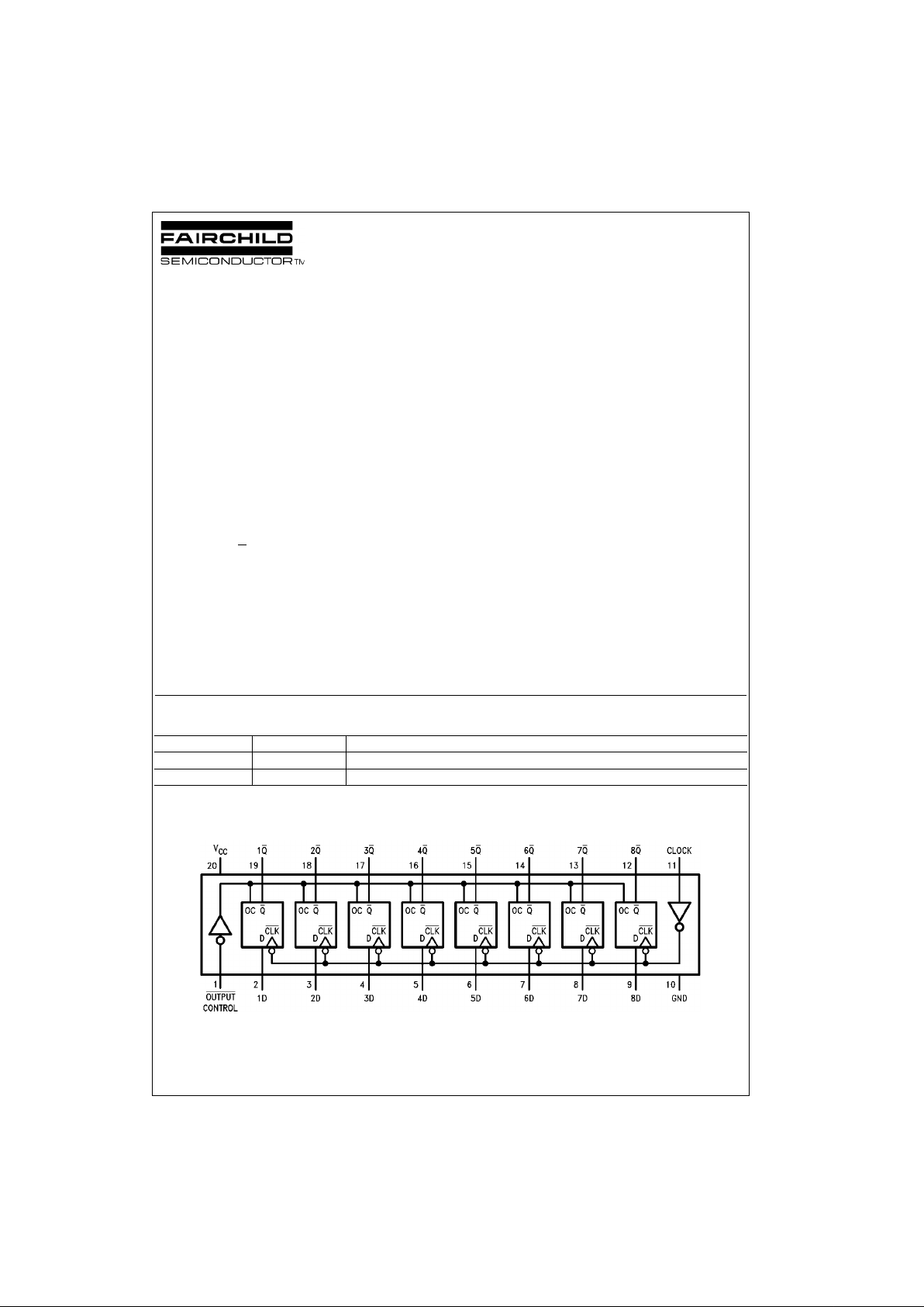
The eight flip-flops of the DM74ALS564A are edge-triggered inverting D-type flip-fl ops. On the positive transition
of the clock, the Q
outputs will be set to the complement of
the logic states that were set up at the D inputs.
A buffered output control input ca n be used to place the
eight outputs in either a normal l ogic state (HIGH or LOW
logic levels) or a high-impedance state. In the high-impedance state the outputs ne ither load nor dr ive the bus lines
significantly.
The output control does not affect the i nternal oper ation of
the flip-flops. That is, the old data can be retained or new
data can be entered even while the outputs are OFF.
Features
■ Switching specifications at 50 pF
■ Switching specifications guaranteed over full tempera-
ture and V
CC
range
■ Advanced oxide-isolated, ion-implanted Schottky TTL
process
■ 3-STATE buffer-type outputs drive bus lines directly
Ordering Code:
Devices also availab le in Tape and Reel. Specify by appending th e s uffix let t er “X” to the ordering code.
Connection Diagram
Order Number Package Number Package Description
DM74ALS564AWM M20B 20-Lead Small Outline Integrated Circuit (SOIC), JEDEC MS-013, 0.300 Wide
DM74ALS564AN N20A 20-Lead Plastic Dual-In-Line Package (PDIP), JEDEC MS-001, 0.300 Wide
www.fairchildsemi.com 2
DM74ALS564A
Function Table
L = LOW State
H = HIGH State
X = Don’t Care
↑ = Positive Edge Transition
Z = High Impedance State
Q
0
= Previous Condit ion of Q
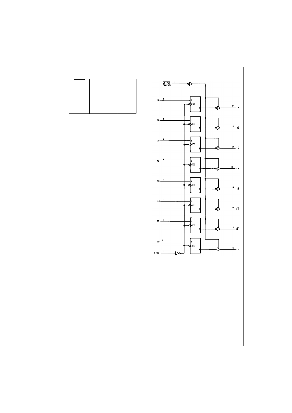
Logic Diagram
Output Clock D Output
Control Q
L ↑ HL
L ↑ LH
LLXQ
0
HXXZ
 Loading...