

Fairchild Semiconductor DM74ALS541WMX, DM74ALS541WM, DM74ALS541SJX, DM74ALS541SJ, DM74ALS541N Datasheet
© 2000 Fairchild Semiconductor Corporation DS009171 www.fairchildsemi.com
October 1986
Revised February 2000
DM74ALS541 Octal Buffer and Line Driver with 3-STATE Outputs
DM74ALS541
Octal Buffer and Line Driver with 3-STATE Outputs
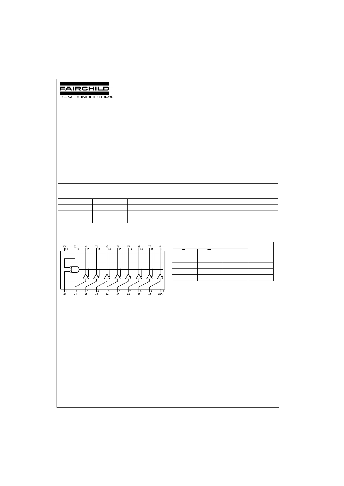
General Description
This octal buffer and line driver is designed to have the performance of the DM74ALS240A serie s and, at the same
time, offer a pinout with inputs and outputs on opposite
sides of the package. Th is arrangement gr eatly enhances
circuit board layout. Th e 3-STATE control gate is a 2-input
NOR such that if either G1 or G 2 is HIGH, a ll eig ht o utputs
are in the high impedance state.
Features
■ Advanced oxide-isolated ion-implanted Schottky TTL
process
■ Switching performan ce is gu aranteed over full tempe rature and V
CC
supply range
■ Data flow-thru pinout (all inputs on opposite side from
outputs)
■ P-N-P Inputs reduce DC loading
Ordering Code:
Devices also availab le in Tape and Reel. Specify by appending th e s uffix let t er “X” to the ordering code.
Connection Diagram Function Table
H = HIGH Logic Level
L = LOW Logic Level
X = Don't Care (Either LOW or HI GH Logic Level)
Hi-Z = High Impedance (OFF) State
Order Number Package Number Package Description
DM74ALS541WM M20B 20-Lead Small Outline Integrated Circuit (SOIC), JEDEC MS-013, 0.300 Wide
DM74ALS541SJ M20D 20-Lead Small Outline Package (SOP), EIAJ TYPE II, 5.3mm Wide
DM74ALS541N N20A 20-Lead Plastic Dual-In-Line Package (PDIP), JEDEC MS-001, 0.300 Wide
Input Output
G
1G2A Y
H X X Hi-Z
X H X Hi-Z
LLLL
LLHH
www.fairchildsemi.com 2
DM74ALS541
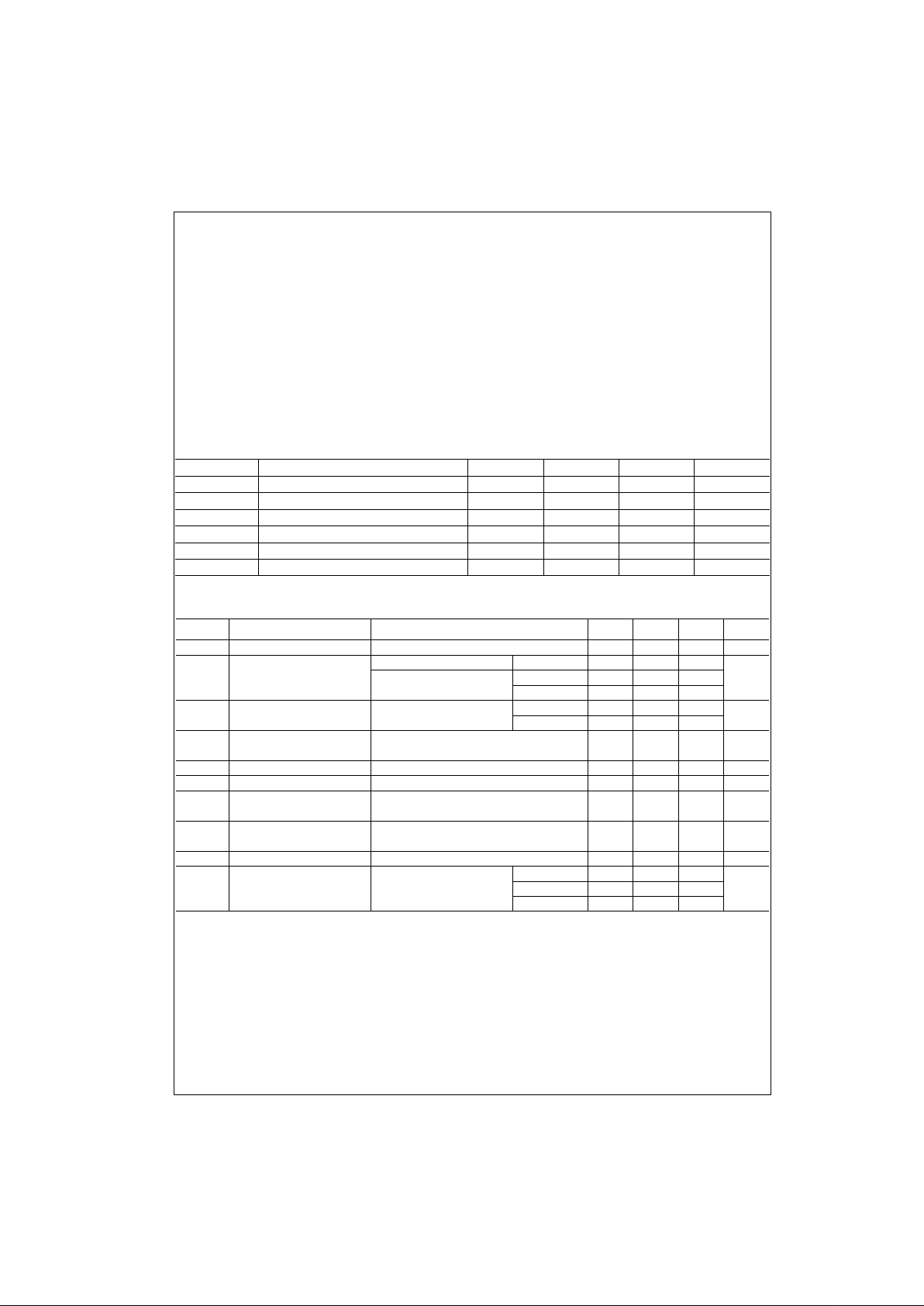
Absolute Maximum Ratings(Note 1)
Note 1: The “Absolute Maximum Ratin gs” are those v alues beyon d which
the safety of the dev ice cannot be guaranteed. T he device sh ould not be
operated at these limits. The parametric values defined in the Electrical
Characteristics tables are not guaranteed at the absolute maximum ratings.
The “Recommend ed O peratin g Cond itions” t able w ill defin e the co ndition s
for actual device operation.
Recommended Operating Conditions
Electrical Characteristics
over recommended free air temperature range
Supply Voltage 7V
Input Voltage: Control Inputs 7V
Voltage Applied to a Disabled
3-STATE Output 5.5V
Operating Free-Air Temperature Range 0°C to +70°C
Storage Temperature Range −65°C to +150°C
Typical θ
JA
N Package 58.5°C/W
M Package 77.5°C/W
Symbol Parameter Min Nom Max Units
V
CC
Supply Voltage 4.5 5 5.5 V
V
IH
HIGH Level Input Voltage 2 V
V
IL
LOW Level Input Voltage 0.8 V
I
OH
HIGH Level Output Current −15 mA
I
OL
LOW Level Output Current 24 mA
T
A
Free Air Operating Temperature 0 70 °C
Symbol Parameter Test Conditions Min Typ Max Units
V
IK
Input Clamp Voltage VCC = Min, II = −18 mA −1.2 V
V
OH
HIGH Level VCC = 4.5V to 5.5V IOH = −0.4 mA VCC − 2
Output Voltage VCC = Min IOH = −3 mA 2.4 3.2 V
IOH = Max 2
V
OL
LOW Level VCC = Min IOL = 12 mA 0.25 0.4
mA
Output Voltage IOL = 24 mA 0.35 0.5
I
I
Input Current at Maximum
VCC = Max, VI = 7V 100 µA
Input Voltage
I
IH
HIGH Level Input Current VCC = Max, VI = 2.7V 20 µA
I
IL
LOW Level Input Current VCC = Max, VI = 0.4V −100 µA
I
OZH
HIGH Level 3-STATE
VCC = Max, VO = 2.7V 20 µA
Output Current
I
OZL
LOW Level 3-STATE
VCC = Max, VO = 0.4V −20 µA
Output Current
I
O
Output Drive Current VCC = Max, VO = 2.25V −30 −112 mA
I
CC
Supply Current VCC = Max Outputs HIGH 6 14
Outputs LOW 15 25 mA
Outputs Disabled 13.5 22
 Loading...