

Fairchild Semiconductor DM74ALS5245WMX, DM74ALS5245WM, DM74ALS5245SJX, DM74ALS5245N Datasheet
DM74ALS5245
Octal 3-STATE Transceiver
DM74ALS5245 Octal 3-STATE Transceiver
October 1986
Revised February 2000
General Description
This octal bus transceiver is designed for asynchronous
two-way communicatio n between data buses. The inputs
include hysteresis which provides improved noise rejection. Data is transmitted either fr om the A bus to the B bus
or from the B bus to the A bus depending on the logic level
of the direction control (D IR) input. T he device can be disabled via the enable inp ut (G
enter the high imped ance mode so the buses are effectively isolated.
) which causes the output s to
Features
■ Input Hysteresis
■ Low output noise generati on
■ High input noise immunity
■ Advanced oxide-isolated, ion implanted Schottky TTL
process
■ Switching specification guarant eed over the full temperature and V
■ PNP inputs to reduce input loading
CC
range
Ordering Code:
Order Number Package Number Package Description
DM74ALS5245WM M20B 20-Lead Small Outline Integrated Circuit (SOIC), JEDEC MS-013, 0.300 Wide
DM74ALS5 245SJ M20D 20-Lead Small Outline Package (SOP), EIAJ TYPE II, 5.3mm Wide
DM74ALS5245N N20A 20-Lead Plastic Dual-In-Line Package (PDIP), JEDEC MS-001, 0.300 Wide
Devices also availab le in Tape and Reel. Specify by appending th e s uffix let t er “X” to the ordering cod e.
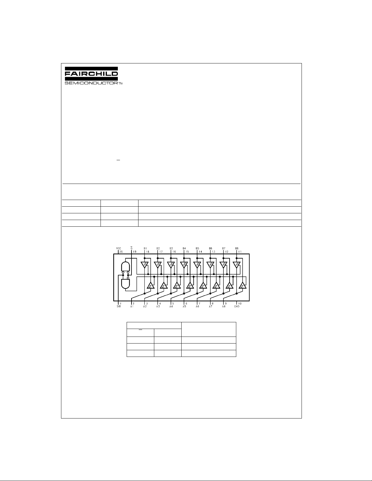
Connection Diagram
Function Table
Control Inputs
G
L L B Data to A Bus
L H A Data to B Bus
H X High Impedance
L = LOW Logic Level H = HIGH Logic Level X = Don't Care (Either LOW or HIGH Logic Lev el)
© 2000 Fairchild Semiconductor Corporation DS009175 www.fairchildsemi.com
DIR
Operation
Absolute Maximum Ratings(Note 1)
Supply Voltage 7V
Input Voltage
Control Inputs 7V
I/O Ports 5.5V
Operating Free-Air Temperature Range 0°C to +70°C
DM74ALS5245
Storage Temperature Range −65°C to +150°C
Typical θ
JA
N Package 56.0°C/W
Note 1: The “Absolute Maximum Ratin gs” are those v alues beyon d which
the safety of the dev ice cannot be guaranteed. T he device sh ould not be
operated at these limits. The parametric values defined in the Electrical
Characteristic tables are not guaranteed at the absolute maximum ratings.
The “Recommend ed O peratin g Cond itions” t able w ill defin e the c ondit ions
for actual device operation.
M Package 74.0°C/W
Recommended Operating Conditions
Symbol Parameter Min Max Units
V
CC
V
IH
V
IL
I
OH
I
OL
T
A
Supply Voltage 4.5 5.5 V
HIGH Level Input Voltage 2 V
LOW Level In put Voltage 0.8 V
HIGH Level Output Current −15 mA
LOW Level Output Current 24 mA
Free Air Operating Temperature Range 0 70 °C
Electrical Characteristics
over recommended free air temperature range. All typical values are measured at VCC = 5V, TA = 25°C.
Symbol Parameter Test Conditions Min Typ Max Units
V
IK
H
YS
V
OH
V
OL
I
I
I
IH
I
IL
I
O
I
CC
V
OLP
V
OLV
V
IHD
V
ILD
Note 2: Plastic DIP package.
Note 3: n = number of device outputs; n−1 outputs switching, each driv en 0V to 3V one output @ G N D .
Note 4: n = number of device outputs; n outputs switching, n−1 inputs s w it c hing 0V to 3V. Input under test switching 3V to thres hold (V
(V
Input Clamp Voltage VCC = Min, II = −18 mA −1.5 V
Hysteresis (VT+ − VT−)VCC = Min 0.2 0.32 V
HIGH Level VCC = 4.5V to 5.5V IOH = −0.4 mA VCC − 2
Output Voltage VCC = Min IOH = −3 mA 2.4 3.2 V
LOW Level VCC = Min IOL = 12 mA 0.25 0.4
Output Voltage IOL = 24 mA 0.35 0.5
Input Current at VCC = Max I/O Ports, VI = 5.5V 100
Maximum Input Voltage Control Inputs, VI = 7V 100
HIGH Level Input Current VCC = Max, VI = 2.7V 20 µA
LOW Level Input Current VCC = Max, VI = 0.4V −100 µA
Output Drive Current VCC = Max, VO = 2.25V −30 −112 mA
Supply Current VCC = Max Outputs HIGH 30 45
Quiet Output Maximum VCC = 5.0V, TA = 25°C
Dynamic V
OL
Quiet Output Minimum VCC = 5.0V, TA = 25°C
Dynamic V
OL
Minimum High Level VCC = 5.0V, TA = 25°C
Dynamic Input Voltage (Note 2)(Note 4)
Maximum Low Level VCC = 5.0V, TA = 25°C
Dynamic Input Voltage (Note 2)(Note 4)
); f = 1 MHz.
IHD
(Figures 1, 2; (Note 2)(Note 3))
(Figures 1, 2; (Note 2)(Note 3))
IOH = Max 2
Outputs LOW 36 55 mA
Outputs Disabled 38 58
0.5 V
−0.2 V
1.6 V
1.0 V
); 0V to threshold
ILD
V
µA
www.fairchildsemi.com 2
Switching Characteristics
over recommended operating free air temperature range
Symbol Parameter Conditions
t
t
t
t
t
t
PLH
PHL
PZH
PZL
PHZ
PLZ
Propagation Delay Time VCC = 4.5V to 5.5V,
LOW-to-HIGH Level Output R1 = R2 = 500Ω,
Propagation Delay Time CL = 50 pF
HIGH-to-LOW Level Output
Output Enable Time
to HIGH Level Output
Output Enable Time
to LOW Level Output
Output Disable Time
from HIGH Level Output
Output Disable Time
from LOW Level Output
From (Input)
To (Output)
A or B to B or A 3 10 ns
A or B to B or A 3 10 ns
G to A or B 5 20 ns
G to A or B 5 20 ns
G to A or B 2 10 ns
G to A or B 4 15 ns
Min Max Units
DM74ALS5245
3 www.fairchildsemi.com
 Loading...