Fairchild Semiconductor DM74ALS257SJX, DM74ALS257SJ, DM74ALS257N, DM74ALS257MX, DM74ALS257M Datasheet

© 2000 Fairchild Semiconductor Corporation DS006227 www.fairchildsemi.com
April 1984
Revised February 2000
DM74ALS257 • DM74ALS258 3-STATE Quad 1-of-2-Line Data Selector/Multiplexer
DM74ALS257 • DM74ALS258
3-STAT E Quad 1-of-2-Line Data Selector/Multiplexer
General Description
These data selectors/multiplexers contain inverters and
drivers to supply full on-chip data selection to the four 3STATE outputs that can interface d ire ctly with data li nes of
bus-organized systems. A 4-b it word selected from one of
two sources is routed to the four outputs. The
DM74ALS257 presents true data whereas the
DM74ALS258 presents inverted data to minimize propagation delay time.
This 3-STATE output feature means that n-bi t (paralleled)
data selectors with up to 258 sou rces can be impl ement ed
for data buses. It also permits the use of standard TTL registers for data retention throughout the system.
Features
■ Switching specifications at 50 pF
■ Switching specifications guaranteed over full tempera-
ture and V
CC
range
■ Advanced oxide-isolated, ion-implanted Schottky TTL
process
■ Functionally and pin for pin compatible with Schottky
and low power Schottky TTL counterpart
■ Improved AC performance over Schottky and low power
Schottky counterparts
■ 3-STAT E buffer-type outputs drive bus lines directly
■ Expand any data input po int
■ Multiplex dual data buses
■ General four functions of two variables (one variable is
common)
■ Source programmable counters
Ordering Code:
Devices also availab le in Tape and Reel. Specify by appending th e s uffix let t er “X” to the ordering code.
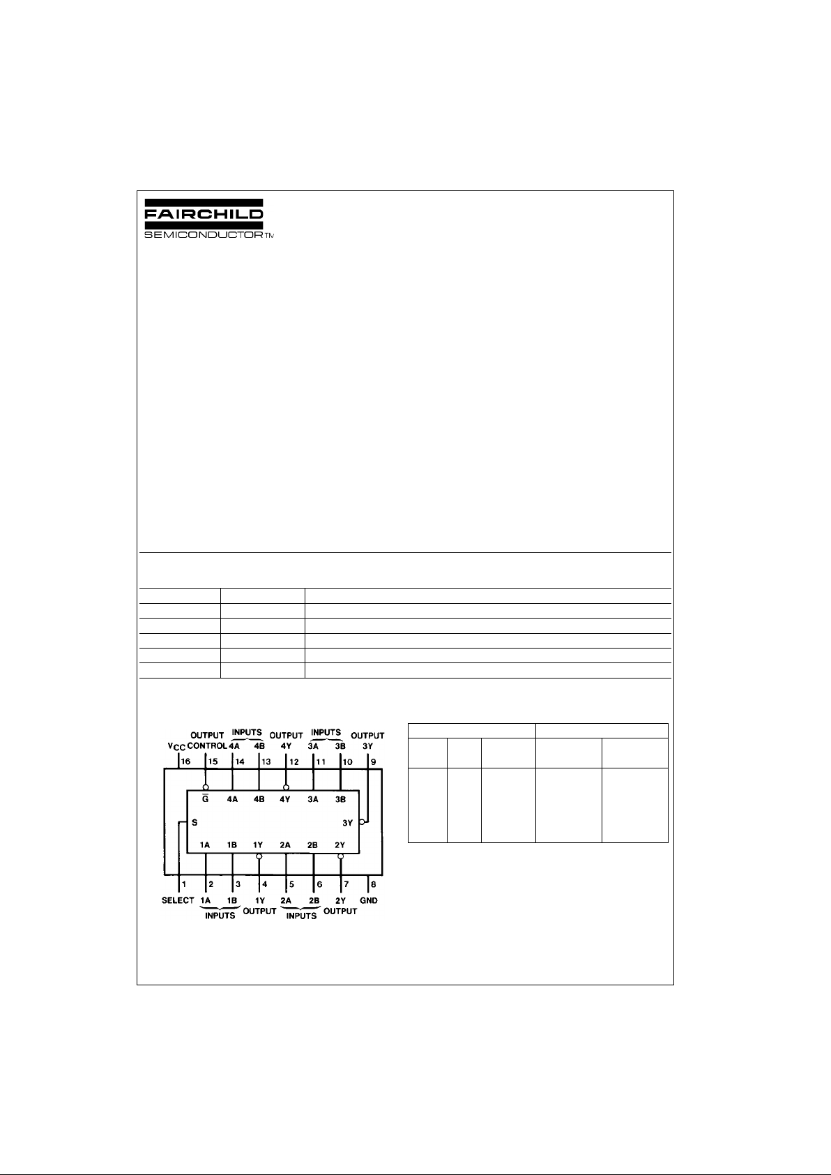
Connection Diagram Function Table
H = HIGH Level
L = LOW Level
X = Don't Care
Z = High Impedance (OF F )
Order Number Package Number Package Description
DM74ALS257M M16A 16-Lead Small Outline Integrated Circuit (SOIC), JEDEC MS-012, 0.150 Narrow
DM74ALS257SJ M16D 16-Lead Small Outline Package (SOP), EIAJ TYPE II, 5.3mm Wide
DM74ALS257N N16E 16-Lead Plastic Dual-In-Line Package (PDIP), JEDEC MS-001, 0.300 Wide
DM74ALS258M M16A 16-Lead Small Outline Integrated Circuit (SOIC), JEDEC MS-012, 0.150 Narrow
DM74ALS258N N16E 16-Lead Plastic Dual-In-Line Package (PDIP), JEDEC MS-001, 0.300 Wide
Inputs Output Y
Output
Select A B DM74ALS257 DM74ALS258
Control
HXXX Z Z
LLLX L H
LLHX H L
LHXL L H
LHXH H L

www.fairchildsemi.com 2
DM74ALS257 • DM74ALS258
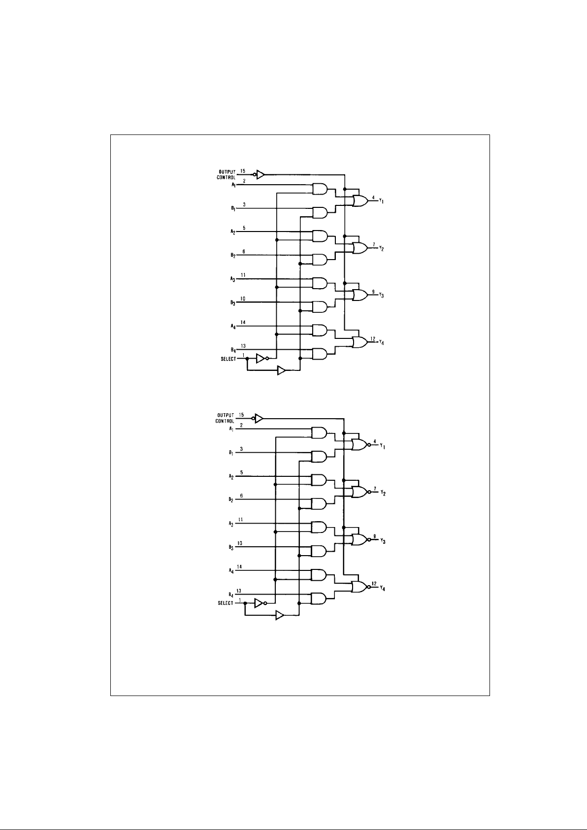
Logic Diagrams
DM74ALS257
DM74ALS258

3 www.fairchildsemi.com
DM74ALS257 • DM74ALS258
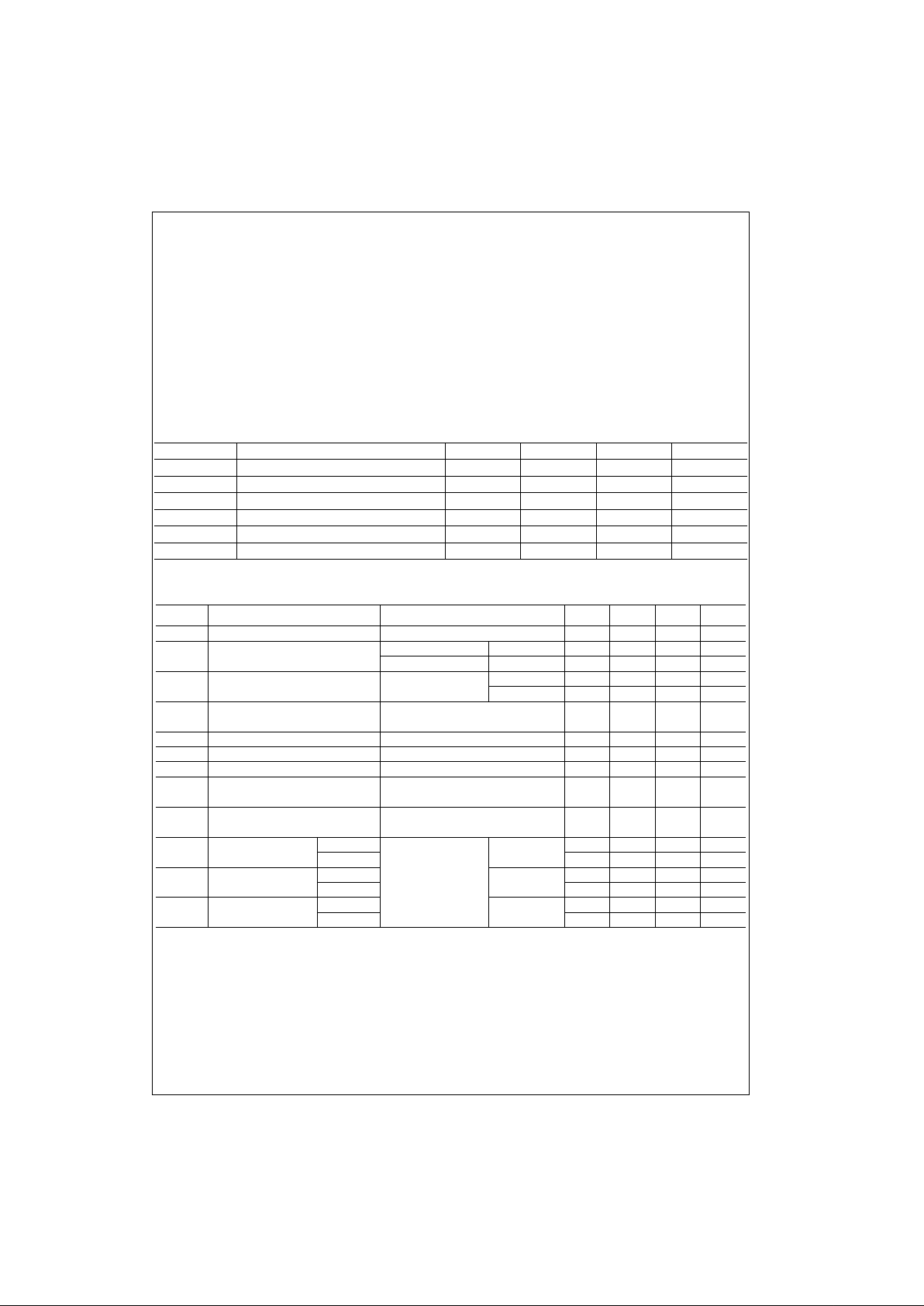
Absolute Maximum Ratings(Note 1)
Note 1: The “Absolute M aximu m R atin gs” are t hose valu es b eyo nd w hich
the safety of the device cannot be guaranteed. The device should not be
operated at these limits. The parametric values defined in the Electrical
Characteristics tables are not guaranteed at the absolute maximum ratings.
The “Recommend ed O peratin g Cond itions” t able w ill defin e the condition s
for actual device operation.
Recommended Operating Conditions
Electrical Characteristics
over recommended operating free air temperature range. All typical values are measured at VCC = 5V, TA = 25°C.
Supply Voltage 7V
Input Voltage 7V
Voltage Applied to Disabled Output 5.5V
OperatingFree Air Temperature Range 0°C to +70°C
Storage Temperature Range −65°C to +150°C
Typical θ
JA
N Package 73.0°C/W
M Package 102.0°C/W
Symbol Parameter Min Nom Max Units
V
CC
Supply Voltage 4.5 5 5.5 V
V
IH
HIGH Level Input Voltage 2 V
V
IL
LOW Level Input Voltage 0.8 V
I
OH
HIGH Level Output Current −2.6 mA
I
OL
LOW Level Output Current 24 mA
T
A
Free Air Operating Temperature 0 70 °C
Symbol Parameter Conditions Min Typ Max Units
V
IK
Input Clamp Voltage VCC = 4.5V, II = −18 mA −1.5 V
V
OH
HIGH Level VCC = 4.5V IOH = −2.6 mA 2.4 3.3 V
Output Voltage IOH = −0.4 mA VCC − 2V
V
OL
LOW Level VCC = 4.5V IOL = 12 mA 0.25 0.4 V
Output Voltage IOL = 24 mA 0.35 0.5 V
I
I
Input Current at Maximum
VCC = 5.5V, VIH = 7V 0.1 mA
Input Voltage
I
IH
HIGH Level Input Current VCC = 5.5V, VIH = 2.7V 20 µA
I
IL
LOW Level Input Current VCC = 5.5V, VIL = 0.4V −0.1 mA
I
O
Output Drive Current VCC = 5.5V, VO = 2.25V −30 −112 mA
I
OZH
OFF-State Output Current VCC = 5.5V,
20 µA
HIGH Level Voltage Applied VO = 2.7V
I
OZL
OFF-State Output Current, VCC = 5.5V,
−20 µA
LOW Level Voltage Applied VO = 0.4V
I
CCH
Supply DM74ALS257 VCC = 5.5V Outputs HIGH 3 6 mA
Current DM74ALS258 Outputs OPEN 2.5 4 mA
I
CCL
Supply DM74ALS257 Outputs LOW 8 12 mA
Current DM74ALS258 7 11 mA
I
CCZ
Supply DM74ALS257 Outputs Disabled 9 14 mA
Current DM74ALS258 8 13 mA
 Loading...