

Fairchild Semiconductor DM74ALS251SJX, DM74ALS251SJ, DM74ALS251N, DM74ALS251MX, DM74ALS251M Datasheet
© 2000 Fairchild Semiconductor Corporation DS006214 www.fairchildsemi.com
April 1984
Revised April 2000
DM74ALS251 3-STATE 1-of-8 Line Data Selector/Multiplexer
DM74ALS251
3-STATE 1-of-8 Line Data Selector/Multiplexer
General Description
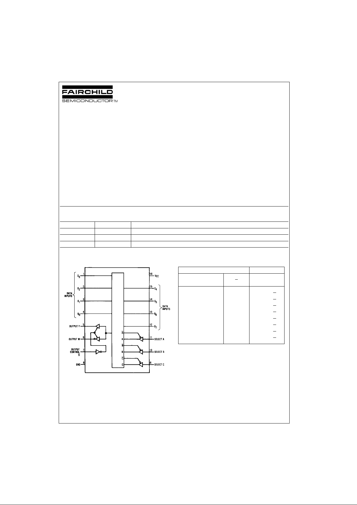
This Data Selector/Mu ltiplexer con tains full on- chip decoding to select one-of-eight data sources as a result of a
unique three-bit binary code at the Select inputs. Two complementary outputs pro vide both inverting and no n-inverting buffer operation. An Out put Control input is provided
which, when at the high level, p laces both outputs in the
high impedance OFF-State. In order to prevent bus access
conflicts, output disable times are shorter than output
enable times. The Select in put buffers incorpor ate internal
overlap features to ensure that select input changes do not
cause invalid output transients.
Features
■ Advanced oxide-isolated, ion-implanted Schottky TTL
process
■ Switching perform ance is guarant eed over full tem perature and V
CC
supply range
■ Pin and functional compatible with LS family counterpart
■ Improved output transient handling capability
■ Output control circuit ry incorporates po wer-up 3-STATE
feature
Ordering Code:
Devices also availab le in Tape and Reel. Specify by appending th e s uffix let t er “X” to the ordering code.
Connection Diagram Function Table
H = HIGH Level
L = LOW Level
X = Don't Care
Z = High Impedance (OFF)
D0 thru D7 = The Level of th e R es pective D Input
Order Number Package Number Package Description
DM74ALS251M M16A 16-Lead Small Outline Integrated Circuit (SOIC), JEDEC MS-012, 0.150 Narrow
DM74ALS251SJ M16D 16-Lead Small Outline Package (SOP), EIAJ TYPE II, 5.3mm Wide
DM74ALS251N N16E 16-Lead Plastic Dual-In-Line Package (PDIP), JEDEC MS-001, 0.300 Wide
Inputs Outputs
Select Strobe
CBA S
YW
XXX H Z Z
LLL L D
0
D
0
LLH L D1D
1
LHL L D2D
2
LHH L D3D
3
HLL L D4D
4
HLH L D5D
5
HHL L D6D
6
HHH L D7D
7
www.fairchildsemi.com 2
DM74ALS251
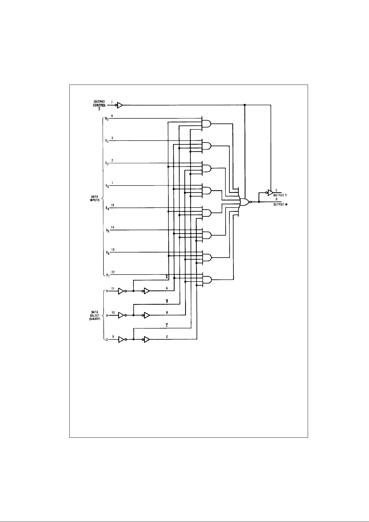
Logic Diagram
3 www.fairchildsemi.com
DM74ALS251
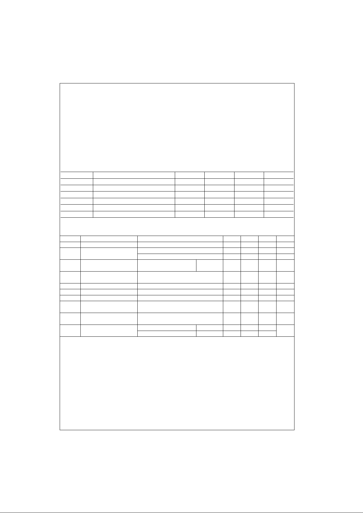
Absolute Maximum Ratings(Note 1)
Note 1: The “Absolute Maximum Ratings” are those values beyo nd whic h
the safety of the dev ice cannot b e guaranteed . The device sh ould not be
operated at these limit s. The parametric values defi ned in the Electrical
Characteristics tabl es are not guara nteed at the absolute maxim um ratings.
The “Recomm ended O peratin g Cond itions ” table will defin e the condition s
for actual device operation.
Recommended Operating Conditions
Electrical Characteristics
over recommended operating free air temperature range. All typical values are measured at V
CC
= 5V, T
A
= 25°C.
Supply Voltage, V
CC
7V
Input Voltage 7V
Voltage Applied to Disabled Output 5.5V
Operating Free Air Temperature Range 0°C to +70°C
Storage Temperature Range −65°C to +150°C
Typical θ
JA
N Package 78.0°C/W
M Package 107.0°C/W
Symbol Parameter Min Nom Max Units
V
CC
Supply Voltage 4.5 5 5.5 V
V
IH
HIGH Level Input Voltage 2 V
V
IL
LOW Level Input Voltage 0.8 V
I
OH
HIGH Level Output Current −2.6 mA
I
OL
LOW Level Output Current 24 mA
T
A
Free Air Operating Temperature 0 70 °C
Symbol Parameter Conditions Min Typ Max Units
V
IK
Input Clamp Voltage VCC = 4.5V, IIN = −18 mA −1.5 V
V
OH
HIGH Level VCC = 4.5V, IOH = Max 2.4 3.2 V
Output Voltage I
OH
= −400 µA, VCC = 4.5V to 5.5V VCC−2V
V
OL
LOW Level
VCC = 4.5V IOL = 24 mA 0.35 0.5 V
Output Voltage
I
I
Input Current at Maximum
V
CC
= 5.5V, VIH = 7V 0.1 mA
Input Voltage
I
IH
HIGH Level Input Current VCC = 5.5V, VIH = 2.7V 20 µA
I
IL
LOW Level Input Current VCC = 5.5V, VIN = 0.4V −0.1 mA
I
O
Output Drive Current VCC = 5.5V, V
OUT
= 2.25V −30 −112 mA
I
OZH
OFF-State Output
V
CC
= 5.5V, V
OUT
= 2.7V 20 µA
Current, HIGH Bias
I
OZL
OFF-State Output
VCC = 5.5V, V
OUT
= 0.4V −20 µA
Current, LOW Bias
I
CC
Supply Current VCC = 5.5V, Inputs = GND Enabled 7 10
mA
Inputs = 4.5V, VCC = 5.5V Disabled 9.4 14
 Loading...