

Fairchild Semiconductor DM74ALS245AWMX, DM74ALS245AWM, DM74ALS245ASJX, DM74ALS245ASJ, DM74ALS245AN Datasheet
...
© 2000 Fairchild Semiconductor Corporation DS006213 www.fairchildsemi.com
September 1986
Revised February 2000
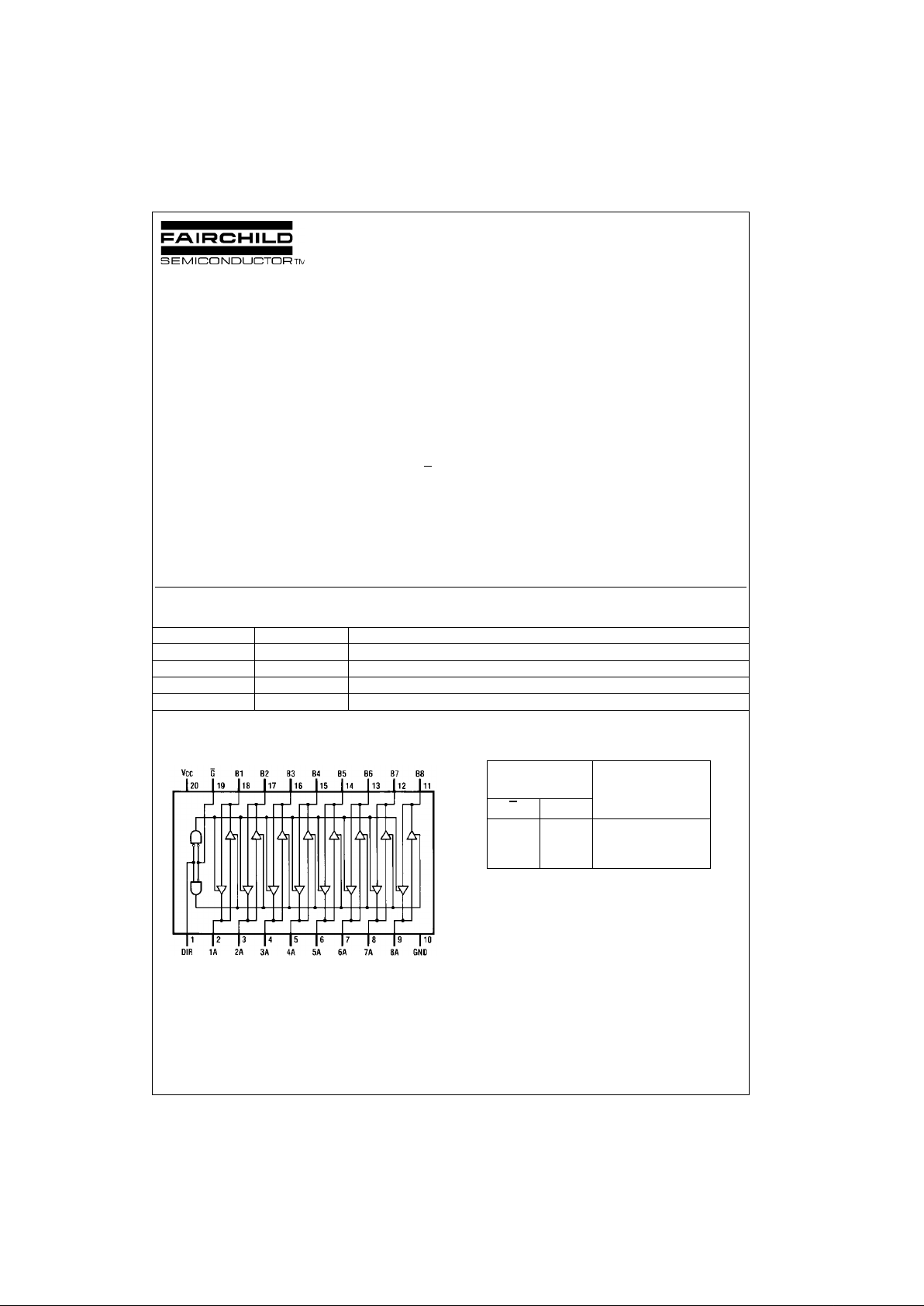
DM74ALS245A Octal 3-STATE Bus T ransceiver
DM74ALS245A
Octal 3-STATE Bus Transceiver
General Description
This advanced low power Schot tky dev ice contains 8 pa irs
of 3-STATE logic elements configured as octal bu s transceivers. These circuits are de signed for use in memory,
microprocessor systems an d in asynch ronou s bidir ectional
data buses. Two way communication between buses is
controlled by the (DIR) input. Data transmits either from the
A bus to the B bus or from the B bus to the A bus. Both the
driver and receiver outputs can be disabled via the (G
)
enable input which causes outputs to enter the high impedance mode so that the buses are effectively isolated.
Features
■ Advanced oxide-isolated, ion-implanted Schottky TTL
process
■ Non-inverting logic output
■ Glitch free bus during power up and down
■ 3-STAT E outputs independently controlled on A and B
buses
■ Low output impedance to drive terminate d transmission
lines to 133Ω
■ Switching response specified into 500Ω/50 pF
■ Specified to interface with CMOS at V
OH
= VCC − 2V
■ PNP inputs to reduce input loading
■ Switching specifications guaranteed over full tempera-
ture and V
CC
range
Ordering Code:
Devices also availab le in Tape and Reel. Specify by appending th e s uffix let t er “X” to the ordering code.
Connection Diagram Function Table
H = HIGH Logic Level
L = LOW Logic Level
X = Either HIGH or LOW Logi c L ev el
Order Number Package Number Package Description
DM74ALS245AWM M20B 20-Lead Small Outline Integrated Circuit (SOIC), JEDEC MS-013, 0.300 Wide
DM74ALS245ASJ M20D 20-Lead Small Outline Package (SOP), EIAJ TYPE II, 5.3mm Wide
DM74ALS245AMSA MSA20 20-Lead Shrink Small Outline Package (SSOP), EIAJ TYPE II, 5.3mm Wide
DM74ALS245AN N20A 20-Lead Plastic Dual-In-Line Package (PDIP), JEDEC MS-001, 0.300 Wide
Control
Inputs Operation
G
DIR
L L B Data to A Bus
L H A Data to B Bus
H X Hi-Z
www.fairchildsemi.com 2
DM74ALS245A
Absolute Maximum Ratings(Note 1)
Note 1: The “Absolute Maximum Ratings” are those values beyond which
the safety of the dev ice cannot be guaranteed. T he device sh ould not be
operated at these limits. The parametric values defined in the Electrical
Characteristics tables are not guaranteed at the absolute maximum ratings.
The “Recommend ed O peratin g Cond itions” t able w ill defin e the co ndition s
for actual device operation.
Recommended Operating Conditions
Electrical Characteristics
over recommended operating free air temperature range. All typical values are measured at VCC = 5V, TA = 25°C.
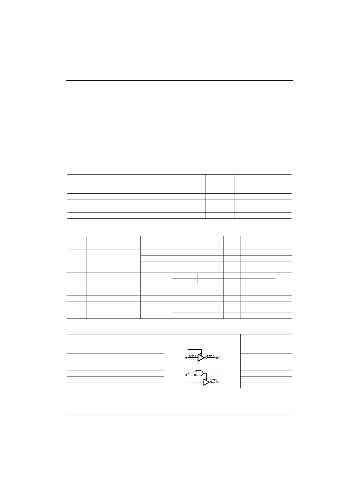
Switching Characteristics (Note 2)
over recommended operating free air temperature range
Note 2: Switching c haracteristic conditi ons are VCC = 4.5V to 5.5V, RL = 500Ω, CL = 50 pF.
Supply Voltage 7V
Input Voltage
Control Inputs 7V
I/O Ports 5.5V
Operating Free Air Temperature Range 0°C to +70°C
Storage Temperature Range −65°C to +150°C
Typical θ
JA
N Package 53.0°C/W
M Package 72.0°C/W
Symbol Parameter Min Typ Max Units
V
CC
Supply Voltage 4.5 5 5.5 V
V
IH
HIGH Level Input Voltage 2 V
V
IL
LOW Level Input Voltage 0.8 V
I
OH
HIGH Level Output Current −15 mA
I
OL
LOW Level Output Current 24 mA
T
A
Operating Free Air Temperature 0 70 °C
Symbol Parameter Conditions Min Typ Max Units
V
IK
Input Clamp Voltage VCC = 4.5V, IIN = −18 mA −1.5 V
V
OH
HIGH Level VCC = 4.5V, IOH = −3 mA 2.4 3.2 V
Output Voltage VCC = 4.5V, IOH = Max 2 2.3 V
IOH = −0.4 mA, VCC = 4.5V to 5.5V VCC − 2V
V
OL
LOW Level Output Voltage VCC = 4.5V IOL = 24 mA 0.35 0.5 V
I
I
Input Current at Maximum VCC = 5.5V VIN = 7V Control Inputs 0.1
mA
Input Voltage VIN = 5.5V A or B Ports 0.1
I
IH
HIGH Level Input Current VCC = 5.5V, VIN = 2.7V 20 µA
I
IL
LOW Level Input Current VCC = 5.5V, VIN = 0.4V −0.1 mA
I
O
Output Drive Current VCC = 5.5V, V
OUT
= 2.25V −30 −112 mA
I
CC
Supply Current VCC = 5.5V Outputs HIGH 30 45 mA
Outputs LOW 36 55 mA
3-STATE 38 58 mA
Symbol Parameter Circuit Configuration Min Max Units
t
PLH
Propagation Delay Time
310ns
LOW-to-HIGH Level Output
t
PHL
Propagation Delay Time
310ns
HIGH-to-LOW Level Output
t
PZL
Output Enable Time to LOW Level 5 20 ns
t
PZH
Output Enable Time to HIGH Level 5 20 ns
t
PLZ
Output Disable Time from LOW Level 4 15 ns
t
PHZ
Output Disable Time from HIGH Level 2 10 ns
 Loading...