

Fairchild Semiconductor DM74ALS165MX, DM74ALS165M, DM74ALS165N Datasheet
DM74ALS165
8-Bit Parallel In/Serial Out Shift Register
DM74ALS165 8-Bit Parallel In/Serial Out Shift Register
January 1986
Revised February 2000
General Description
The DM74ALS165 is an 8-bit serial register that, when
clocked, shifts the data toward serial output, Q
access to each stage is provid ed by eight individu al direct
data inputs that are enabled by a low le vel at the SH/LD
input. The DM74ALS 165 a lso feat ures a clo ck inhibit fun ction and a complemented serial output, Q
.
H
. Parallel-in
H
Features
■ Complementary outputs
■ Direct overriding load (data) inputs
■ Gated clock inputs
■ Parallel-to-serial data conversion
Clocking is accomplished by a LOW-to-HIGH transition of
the CLK input while SH/LD
is held HIGH and CLK INH is
held LOW. The functions of the C LK and CLK INH (clock
inhibit) inputs are interchangeable. Since a LOW CLK input
and a LOW-to-HIGH transition of CLK INH will also accomplish clocking, CLK INH should be changed to the high
level only while the CLK input is HIGH. Parallel loading is
inhibited when SH/L D
the register are enabled while SH/LD
is held HIGH. The parallel inputs to
is LOW indepen-
dently of the levels of CLK, CLK INH, or SER inputs.
Ordering Code:
Order Number Package Number Package Description
DM74ALS165M M16A 16-Lead Small Outline Integrated Circuit (SOIC), JEDEC MS-012, 0.150 Narrow
DM74ALS165N N16E 16-Lead Plastic Dual-In-Line Package (PDIP), JEDEC MS-001, 0.300 Wide
Devices also availab le in Tape and Reel. Specify by appending th e s uffix let t er “X” to the ordering cod e.
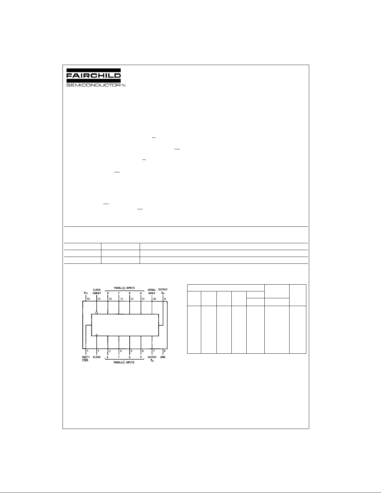
Connection Diagram Function Table
Inputs Internal
Shift/ Clock Clock Serial Parallel Outputs Output
Load Inhibit
L X X X a...h a b h
HL LX XQ
HL ↑ HXHQAnQ
HL ↑ LXLQAnQ
H ↑ LH XHQAnQ
H ↑ LL XLQAnQ
HHXX XQA0QB0Q
H = HIGH Level (steady-state),
L = LOW Level (stea dy -state)
X = Don't Care (any input, including transitions)
↑ = Transition from LOW-to-HIGH level
a...h = The level of steady-state input at inputs A through H, respectively
, QB0, QH0 = The level of QA, QB, or QH, respectively, before the
Q
A0
indicated steady-s ta t e input conditions were es t ablished
, QGn = The level of QA or QG, respectively, before the most recent
Q
An
↑ transition of the clock
A...H Q
AQBQH
A0QB0QH0
Gn
Gn
Gn
Gn
H0
© 2000 Fairchild Semiconductor Corporation DS006712 www.fairchildsemi.com
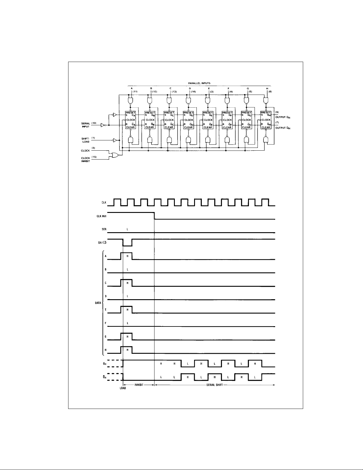
Logic Diagram
DM74ALS165
Timing Diagram
Typical Shift, Load, and Inhibit Sequences
www.fairchildsemi.com 2
 Loading...