Fairchild Semiconductor DM74ALS151N, DM74ALS151MX, DM74ALS151M Datasheet

© 2000 Fairchild Semiconductor Corporation DS006203 www.fairchildsemi.com
April 1984
Revised February 2000
DM74ALS151 1 of 8 Line Data Selector/Multiplexer
DM74ALS151
1 of 8 Line Data Selector/Multiplexer
General Description
This Data Selector/Multi plexer contain s full on-chip decoding to select one-of-eight data sources as a result of a
unique three-bit binary code at the Select inputs. Two complementary outputs pro vide both inverting and no n-inverting buffer operation. A Strobe input is provided which,
when at the high level, disable s all data inputs and forces
the Y output to the LOW state and the W output to the
HIGH state. The Select input buffers incorporate internal
overlap features to ensure that select input changes do not
cause invalid output transients.
Features
■ Advanced oxide-isolated, ion-implanted Schottky TTL
process
■ Switching performan ce is gu aranteed over full tempe rature and V
CC
supply range
■ Pin and functional compatible with LS family counterpart
■ Improved output transient handling capability
Ordering Code:
Devices also availab le in Tape and Reel. Specify by appending th e s uffix let t er “X” to the ordering code.
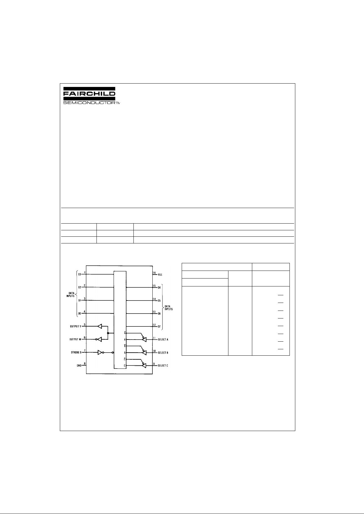
Connection Diagram Function Table
H = HIGH Level
L = LOW Level
X = Don't Care
D0 thru D7 = the level of the respective D input
Order Number Package Number Package Description
DM74ALS151M M16A 16-Lead Small Outline Integrated Circuit (SOIC), JEDEC MS-012, 0.150 Narrow
DM74ALS151N N16E 16-Lead Plastic Dual-In-Line Package (PDIP), JEDEC MS-001, 0.300 Wide
Inputs Outputs
Select Strobe
YW
CBA S
XXX H L H
LLL L D0D0
L L H L D1 D1
L H L L D2 D2
L H H L D3 D3
H L L L D4 D4
H L H L D5 D5
H H L L D6 D6
HHH L D7 D7

www.fairchildsemi.com 2
DM74ALS151
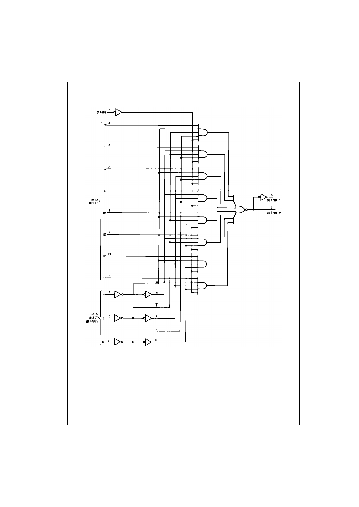
Logic Diagram
 Loading...