

Fairchild Semiconductor DM74ALS125N, DM74ALS125MX, DM74ALS125M Datasheet
© 2000 Fairchild Semiconductor Corporation DS010620 www.fairchildsemi.com
November 1989
Revised February 2000
DM74ALS125 Quad 3-STATE Buffer
DM74ALS125
Quad 3-STATE Buffer
General Description
This device contains four independent gates each of which
performs a non-invertin g buffer function . The outpu ts have
the 3-STATE feature. The 3-STATE circuitry contains a fea ture that maintains the buffer outputs in 3-STATE (high
impedance state) during pow er supply ramp-up or rampdown. This eliminates bus glitching problems that arise
during power-up and p ower-down. To minimize the possibility that two outputs will attempt to take a co mmon bus to
opposite logic levels, t he disable time is short er than the
enable time of the outputs.
Features
■ Advanced low power oxide-isolated ion-implanted
Schottky TTL process
■ Functional and pin compatible with the 74LS counterpart
■ Switching response specified into 500Ω and 50 pF load
■ Switching response specific ations guaranteed over full
temperat ure and V
CC
supply range
■ PNP input design reduces input loading
■ Low level drive current: 74ALS = 24 mA
Ordering Code:
Devices also availab le in Tape and Reel. Specify by appending th e s uffix let t er “X” to the ordering code.
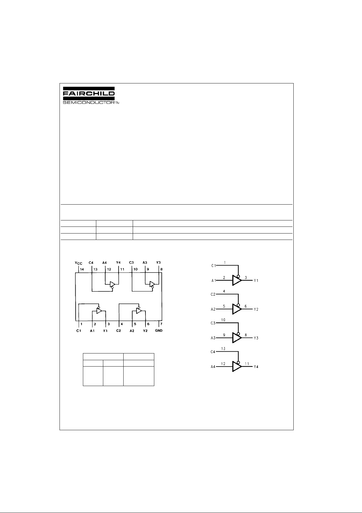
Connection Diagram
Functional Table
Y = A
H = HIGH Logic Level
L = LOW Logic Level
X = Either LOW or HIGH Logic Level
Hi-Z = 3-STATE (Outputs are disabled)
Logic Diagram
Order Number Package Number Package Description
DM74ALS125M M14A 14-Lead Small Outline Integrated Circuit (SOIC), JEDEC MS-012, 0.150 Narrow
DM74ALS125N N14A 14-Lead Plastic Dual-In-Line Package (PDIP), JEDEC MS-001, 0.300 Wide
Input Output
AC Y
LL L
HL H
X H Hi-Z

www.fairchildsemi.com 2
DM74ALS125
Absolute Maximum Ratings(Note 1)
Note 1: The Absolute Maximum Ratings are those values beyond which
the safety of the dev ice cannot be guaranteed. T he device sh ould not be
operated at these limits. The parametric values defined in the Electrical
Characteristics tables are not guaranteed at the absolute maximum ratings.
The “Recommend ed O peratin g Cond itions” t able w ill defin e the co ndition s
for actual device operation.
Recommended Operating Conditions
Electrical Characteristics
over recommended operating free air temperature (unless otherwise specified)
Supply Voltage, V
CC
7V
Input Voltage 7V
Voltage Applied to Disabled Output 5.5V
Operating Free Air Temperature Range 0 to +70°C
Storage Temperature Range −65°C to +150°C
Typical θ
JA
N Package 78.0°C/W
M Package 111.0°C/W
Symbol Parameter Min Typ Max Units
V
CC
Supply Voltage 4.5 5 5.5 V
V
IH
HIGH Level Input Voltage 2 V
V
IL
LOW Level Input Voltage 0.8 V
I
OH
HIGH Level Output Current −15 mA
I
OL
LOW Level Output Current 24 mA
T
A
Operating Free-Air Temperature 0 70 °C
Symbol Parameter Conditions Min Typ Max Units
V
IK
Input Clamp Voltage VCC = 4.5V, II = −18 mA −1.5 V
V
OH
HIGH Level VCC = 4.5V to 5.5V IOH = −0.4 mA VCC − 2V
Output Voltage VCC = 4.5V IOH = −3 mA 2.4 V
IOH = Max 2 V
V
OL
LOW Level VCC = 4.5V IOL = 12 mA 0.25 0.4 V
Output Voltage IOL = 24 mA 0.35 0.5 V
I
I
Input Current at Max
VCC = 5.5V, VI = 7V 0.1 mA
Input Voltage
I
IH
HIGH Level
VCC = 5.5V, VI = 2.7V 20 µA
Input Current
I
IL
LOW Level
VCC = 5.5V, VIL = 0.4V −0.1 mA
Input Current
I
O
Output Drive
VCC = 5.5V, VO = 2.25V −30 −112 mA
Current
I
OZH
HIGH Level 3-STATE
VCC = 5.5V, VO = 2.7V 20 µA
Output Current
I
OZL
LOW Level 3-STATE
VCC = 5.5V, VO = 0.4V −20 µA
Output Current
I
CC
Supply Current VCC = 5.5V Outputs HIGH 7 10 mA
Outputs LOW 10 14 mA
3-STATE 13.5 18 mA
 Loading...