Fairchild Semiconductor CD4013BCSJX, CD4013BCSJ, CD4013BCN, CD4011BCSJX, CD4013BCMX Datasheet
...
October 1987
Revised January 1999
CD4013BC Dual D-Type Flip-Flop
© 1999 Fairchild Semiconductor Corporation DS005946.prf www.fairchildsemi.com
CD4013BC
Dual D-Type Flip-Flop
General Description
The CD4013B dual D- type flip-flo p is a monol ithic comp lementary MOS (CMOS ) integrated circuit constructed w ith
N- and P-channel enhancement mode transistors. Each
flip-flop has indepen dent data, set, re set, and clo ck inputs
and “Q” and “Q
” outputs. These devices can be use d for
shift register application s, and by connecting “Q
” output to
the data input, for counter and toggle applications. The
logic level present at the “D” input is transferred to the Q
output during the positive-going transition of the clock
pulse. Setting or resetting is indepen dent of the clock and
is accomplished by a high level on the set or reset line
respectively.
Features
■ Wide supply voltage range: 3.0V to 15V
■ High noise immunity: 0.45 V
DD
(typ.)
■ Low power TTL: fan out of 2 driving 74L
compatibility: or 1 driving 74LS
Applications
• Automotive
• Data terminals
• Instrumentation
• Medical electronics
• Alarm system
• Industrial electronics
• Remote metering
• Computers
Ordering Code:
Devices also available in Tape and Reel. Specify by appending the suffix letter “X” to the ordering code.
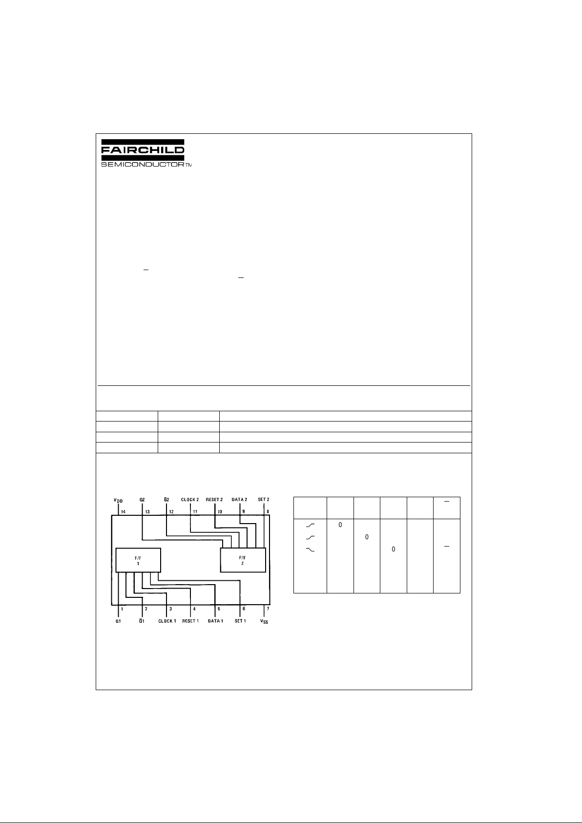
Connection Diagram
Pin Assignments for DIP, SOIC and SOP
Top View
Truth Table
No Change
x = Don't Care Case
Note 1: Level Change
Order Number Package Number Package Description
CD4013BCM M14A 14-Lead Small Outline Integrated Circuit (SOIC), JEDEC MS-120, 0.150” Narrow
CD4013BCSJ M14D 14-Lead Small Outline Package (SOP), EIAJ TYPE II, 5.3mm Wide
CD4013BCN N14A 14-Lead Dual-In-Line Package (PDIP), JEDEC MS-001, 0.300” Wide
CL
(Note 1)
DRSQQ
00001
10010
x00QQ
x x1001
x x0110
x x1111

www.fairchildsemi.com 2
CD4013BC
Schematic Diagrams
Logic Diagram
 Loading...