Fairchild Semiconductor 74LVTH240WM, 74LVTH240SJX, 74LVTH240SJ, 74LVTH240MTCX, 74LVTH240MTC Datasheet
...
74LVT240 • 74LVTH240
Low Voltage Octal Buffer/Line Driver
with 3-STATE Outputs
74LVT240 • 74LVTH240 Low Voltage Octal Buffer/Line Driver with 3-STATE Outputs
July 1999
Revised August 1999
General Description
The LVT240 and LVTH240 are inverting octal buffe rs and
line drivers designed to be employed as memory addr ess
drivers, clock drivers and bus oriented transmitters or
receivers which provides improved PC board density.
The LVTH240 data inputs include b ushold, eliminati ng the
need for external pull-up resistors to hold unused inputs.
These octal buffers and line drivers are designed for lowvoltage (3.3V) V
provide a TTL interface to a 5V environment. The LVT240
and LVTH240 are fabricated with an advanced BiCMOS
technology to achiev e high speed operation similar to 5V
ABT while maintaining low power dissipation.
applications, but wi th the capability to
CC
Features
■ Input and output interface capability to systems at
5V V
CC
■ Bushold data inputs elimina te the nee d for exte rnal pullup resistors to hold unused inputs (74LVTH240), also
available without bushold feature (74LVT240).
■ Live insertion/extraction per mitt ed
■ Power Up/Down high impedance provides glitch-free
bus loading
■ Outputs source/sink −32 mA/+64 mA
■ Functionally compatible with the 74 series 240
■ Latch-up performance exce eds 500 mA
Ordering Code:
Order Number Package Number Package Description
74LVT240WM M20B 20-Lead Small Outline Integrated Circuit (SOIC), JEDEC MS-013, 0.300 Wide
74LVT240SJ M20D 20-Lead Small Outline Package (SOP), EIAJ TYPE II, 5.3mm Wide
74LVT240MSA MSA20 20-Lead Shrink Small Outline Package (SSOP), EIAJ TYPE II, 5.3mm Wide
74LVT240MTC MTC20 20-Lead Thin Shrink Small Outline Package (TSSOP), JEDEC MO-153, 4.4mm Wide
74LVTH240WM M20B 20-Lead Small Outline Integrated Circuit (SOIC), JEDEC MS-013, 0.300 Wide
74LVTH240SJ M20D 20-Lead Small Outline Package (SOP), EIAJ TYPE II, 5.3mm Wide
74LVTH240MSA MSA20 20-Lead Shrink Small Outline Package (SSOP), EIAJ TYPE II, 5.3mm Wide
74LVTH240MTC MTC20 20-Lead Thin Shrink Small Outline Package (TSSOP), JEDEC MO-153, 4.4mm Wide
Device also available in Tape and Reel. Specify by appending s uffix let te r “X” to the ordering code .
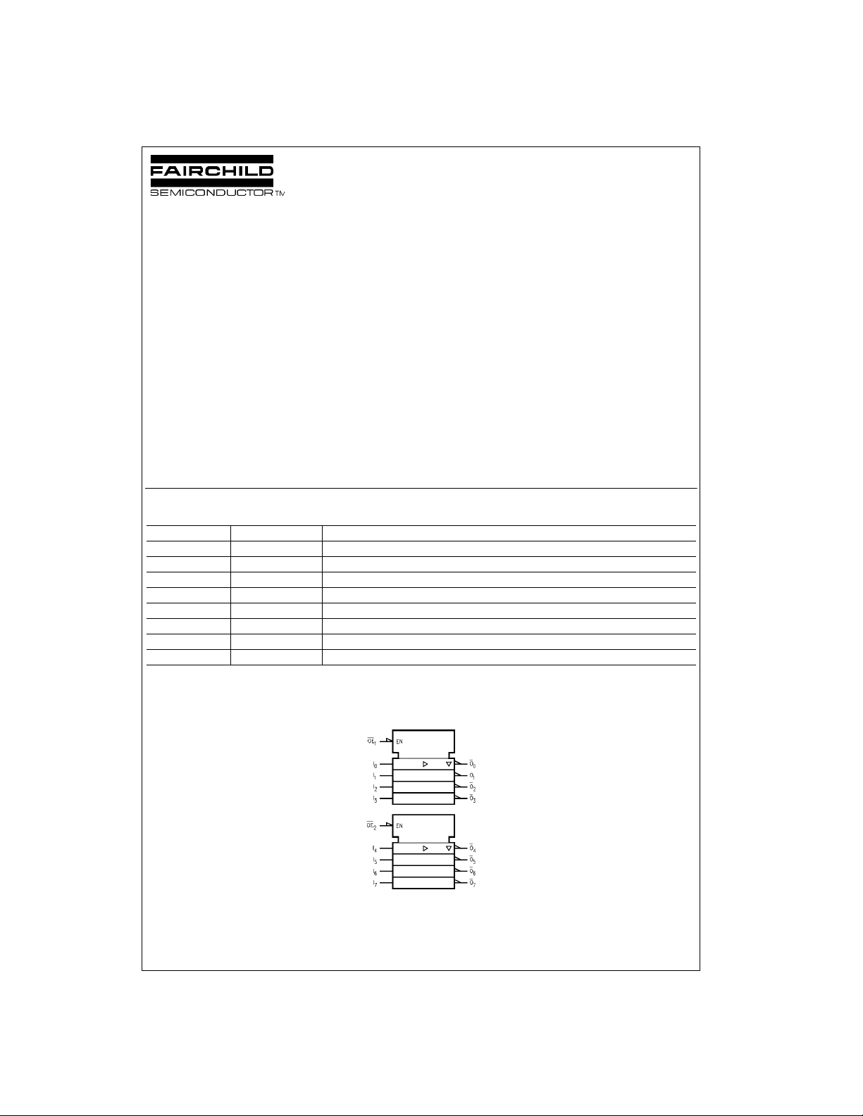
Logic Symbol
IEEE/IEC
© 1999 Fairchild Semiconductor Corporation DS500153 www.fairchildsemi.com

Connection Diagram Pin Descriptions
Pin Names Description
OE
I
0–I7
O
0–O7
74LVT240 • 74LVTH240
Truth Tables
, OE23-STATE Output
1
Enable Inputs
Inputs
3-STATE Outputs
H = HIGH Voltage Level
L = LOW Voltage Level
X = Immaterial
Z = High Impedance
Inputs Outputs
OE
I
1
n
(Pins 12, 14, 16, 18)
LL H
LH L
H X Z
Inputs Outputs
OE
2
I
n
(Pins 3, 5, 7, 9)
LL H
LH L
H X Z
www.fairchildsemi.com 2

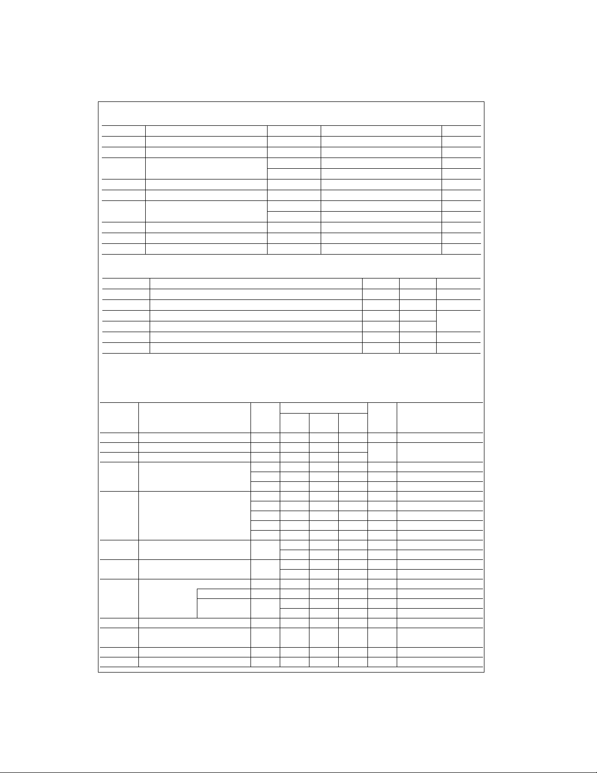
Absolute Maximum Ratings(Note 1)
Symbol Parameter Value Conditions Units
V
CC
V
I
V
O
Supply Voltage −0.5 to +4.6 V
DC Input Voltage −0.5 to +7.0 V
DC Output Voltage −0.5 to +7.0 Output in 3-STATE V
−0.5 to +7.0 Output in HIGH or LOW State (Note 2) V
I
I
I
I
I
T
IK
OK
O
CC
GND
STG
DC Input Diode Current −50 VI < GND mA
DC Output Diode Current −50 VO < GND mA
DC Output Current 64 VO > VCCOutput at HIGH State mA
128 V
> VCC Output at LOW State mA
O
DC Supply Current per Supply Pin ±64 mA
DC Ground Current per Ground Pin ±128 mA
Storage Temperature −65 to +150 °C
Recommended Operating Conditions
Symbol Parameter Min Max Units
V
CC
V
I
I
OH
I
OL
T
A
∆t/∆V Input Edge Rate, V
Note 1: Absolute Maximum continuous ratings are those values beyond which damage to the device may occur. Exposure to these conditions or conditions
beyond those indica te d m ay adversely affect dev ic e reliability. Functional operation under absolute maximum rated conditions is not implied.
Note 2: I
Supply Voltage 2.7 3.6 V
Input Voltage 0 5.5 V
HIGH-Level Output Current −32 mA
LOW-Level Output Current 64
Free-Air Operating Temperature −40 85 °C
= 0.8V–2.0V, VCC = 3.0V 0 10 ns/V
IN
Absolute Maximum Rating must be observed.
O
74LVT240 • 74LVTH240
DC Electrical Characteristics
V
Symbol Parameter
V
IK
V
IH
V
IL
V
OH
V
OL
I
I(HOLD)
(Note 4) −75 µAVI = 2.0V
I
I(OD)
(Note 4) −500 µA (Note 6)
I
I
I
OFF
I
PU/PD
I
OZL
I
OZH
Input Clamp Diode Voltage 2.7 −1.2 V II = −18 mA
Input HIGH Voltage 2.7–3.6 2.0
Input LOW Voltage 2.7–3.6 0.8 VO ≥ VCC − 0.1V
Output HIGH Voltage 2.7–3.6 VCC−0.2 V IOH = −100 µA
Output LOW Voltage 2.7 0.2 V IOL = 100 µA
Bushold Input Minimum Drive 3.0 75 µAVI = 0.8V
Bushold Input Over-Drive
Current to Change State
Input Current 3.6 10 µAVI = 5.5V
Power Off Leakage Current 0 ±100 µA0V ≤ VI or VO ≤ 5.5V
Power up/down 3-STATE 0–1.5V ±100 µAVO = 0.5V to 3.0V
Output Current VI = GND or V
3-STATE Output Leakage Current 3.6 −5 µAVO = 0.5V
3-STATE Output Leakage Current 3.6 5 µAVO = 3.0V
Control Pins 3.6 ±1 µAVI = 0V or V
Data Pins 3.6 −5 µAVI = 0V
CC
(V)
2.7 2 .4 V IOH = −8 mA
3.0 2.0 V IOH = −32 mA
2.7 0.5 V IOL = 24 mA
3.0 0.4 V IOL = 16 mA
3.0 0.5 V IOL = 32 mA
3.0 0.55 V IOL = 64 mA
3.0 500 µA (Note 5)
T A =−40°C to +85°C
Min Typ Max
(Note 3)
Units Conditions
VO ≤ 0.1V or
V
1 µAVI = V
CC
CC
CC
3 www.fairchildsemi.com
 Loading...