Fairchild Semiconductor 74LVTH16952MEAX, 74LVTH16952MEA, 74LVTH16952MTDX, 74LVTH16952MTD Datasheet

74LVTH16952
Low Voltage 16-Bit Registered Transceiver
with 3-STATE Outputs
74LVTH16952 Low Voltage 16-Bit Registered Transceiver with 3-STATE Outputs
January 2000
Revised January 2000
General Description
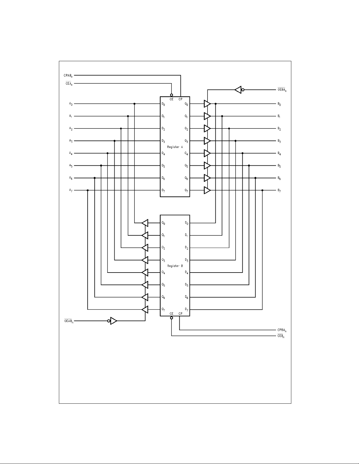
The LVTH16952 is a 16-bit registered transceiver. Two 8bit back to back registers store data flowing in both directions between two bidirectional buses. Separate clock,
clock enable, and outp ut enable signals are provide d for
each register.
The LVTH16952 data inputs includ e bushold, eliminating
the need for external pull-up resistors to hold unused
inputs.
The registered transceiver is designed for low-voltage
(3.3V) V
TTL interface to a 5V environment.
The LVTH16952 is fabricated with an advanced BiCMOS
technology to achiev e high speed operation similar to 5V
ABT while maintaining low power dissipation.
applications, but with the capability to provide a
CC
Features
■ Input and output interface capability to systems at
5V V
CC
■ Bushold data inputs eliminate the need for external
pull-up resistors to hold unused inputs
■ Live insertion/extraction per mitt ed
■ Power Up/Down high impedance provides glitch-free
bus loading
■ Outputs source/sink −32 mA/+64 mA
■ Functionally compatible with the 74 series 16952
■ Latch-up performance exce eds 500 mA
Ordering Code:
Order Number Package Number Package Description
74LVTH16952MEA MS56A 56-Lead Shrink Small Outline Package (SSOP), JEDEC MO-118, 0.300 Wide
74LVTH16952MTD MTD56 56-Lead Thin Shrink Small Outline Package (TSSOP), JEDEC MO-153, 6.1mm Wide
Devices also availab le in Tape and Reel. Specify by appending th e s uffix let t er “X” to the ordering cod e.
© 2000 Fairchild Semiconductor Corporation DS500103 www.fairchildsemi.com

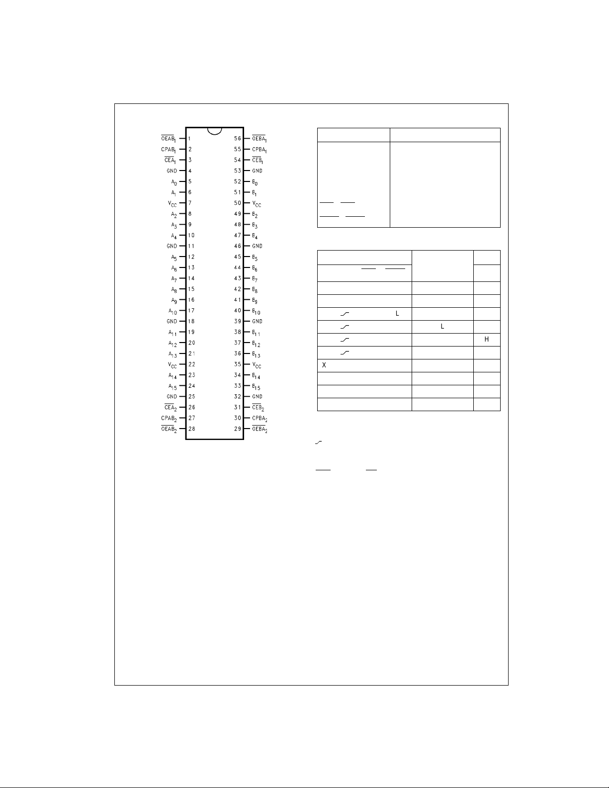
Connection Diagram Pin Descriptions
Pin Names Description
A
0–A16
74LVTH16952
B
0–B16
CPAB
CEA
OEAB
, CPBA
n
, CEB
n
n
n
, OEBA
n
n
Data Register A Inputs
B-Register 3-STATE Outputs
Data Register B Inputs
A-Register 3-STATE Outputs
Clock Pulse Inputs
Clock Enable
Output Enable Inputs
Truth T able
(Note 1)
Inputs Internal Register Output
CPABnCEAnOEAB
A
n
Value
n
XX H L NC B
B
n
0
XX H H NC Z
L
L
H
H
XL X L NC B
XH X L NC B
LL L L
LH L Z
LL H H
LH H Z
0
0
XL X H NC Z
XH X H NC Z
H = HIGH Voltage Level
L = LOW Voltage Level
X = Immaterial
Z = Output High Imped ance
= LOW-to-HIGH Transition.
NC = No Change (state est ablished by last valid CP)
= State established by last valid CP
B
0
Note 1: A to B data flow show n; B to A flow co ntrol is the sam e, but used
, CPBAn and CEBn.
OEBA
n
www.fairchildsemi.com 2

Logic Diagram
74LVTH16952
Note: n for either byte 1 or byte 2.
Please note that thes e diagrams are provide d only for the understan ding of logic operation s a nd should not be used to est im ate propagation delays.
3 www.fairchildsemi.com
 Loading...