Fairchild Semiconductor 74LVTH16835MTDX, 74LVTH16835MTD, 74LVTH16835MEAX, 74LVTH16835MEA Datasheet

Preliminary
© 2000 Fairchild Semiconductor Corporation DS500102 www.fairchildsemi.com
May 2000
Revised May 2000
74LVTH16835 Low Voltage 18-Bit Universal Bus Driver
74LVTH16835
Low Voltage 18-Bit Universal Bus Driver
with 3-STAT E Outputs (Prelimina ry)
General Description
The LVTH16835 consists of 18-bit universal bus drivers
which combine D-type latches and D-type flip-flops to allow
data flow in transparent , latched, or clocked mod es. Data
flow from A to Y is controlled by the outpu t-enable (OE
)
input. This device operates in the transparent mode when
the latch-enable (LE) input is HIGH. The A data is latched if
the clock (CLK) input is h eld at a HIGH or LOW logic l e vel.
If LE is LOW, the A-bus data is stor ed in the latch/ flip-flop
on the LOW-to-HIGH transition of the CLK. When OE
is
HIGH, the outputs are in the high-impedance state.
The LVTH16835 data inputs includ e bushold, eliminating
the need for external pull-up resistors to hold unused
inputs.
The bus driver is designed for low voltage (3.3V) V
CC
appli-
cations, but with the capability to provide a TTL i nterface to
a 5V environment . The LVTH16835 is fabricated with an
advanced BiCMOS technology to achieve high speed operation similar to 5V ABT while maintaining low power dissipation.
Features
■ Input and output interface capability to systems at
5V V
CC
■ Bushold data inputs eliminate the need for external
pull-up resistors to hold unused inputs
■ Live insertion/extraction per mitted
■ Power Up/Down high impedance provides glitch-free
bus loading
■ Outputs source/sink −32 mA/+64 mA
■ Latch-up performance exce eds 500 mA
Ordering Code:
Devices also availab le in Tape and Reel. Specify by appending th e s uffix let t er “X” to the ordering code.
Order Number Package Numb er Package Description
74LVTH16835MEA MS56A 56-Lead Shrink Small Outline Package (SSOP), JEDEC MO-118, 0.300 Wide
74LVTH16835MTD MTD56 56-Lead Thin Shrink Small Outline Package (TSSOP), JEDEC MO-153, 6.1mm Wide

Preliminary
www.fairchildsemi.com 2
74LVTH16835
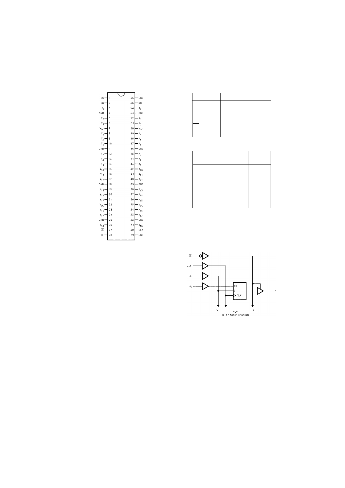
Connection Diagram Pin Descriptions
Tr uth Ta ble
H = HIGH Voltage Level L = LOW Voltage Level
X = Immaterial Z = High Impedance
↑ = HIGH-to-LOW Clock Transition
Note 1: Output level be fore the indicated steady-st ate input conditions
were established, provided that CLK was HI GH before LE went LOW.
Note 2: Output level be fore the indicated steady-st ate input conditions
were established.
Logic Diagram
Pin Names Description
A
1–A18
Data Register Inputs
Y
1–Y18
3-STATE Outputs
CLK Clock Pulse Input
OE
Output Enable Input
LE Latch Enable Input
Inputs
Output
Y
OE
LE CLK A
HXXX Z
LHXL L
LHXH H
LL↑ LL
LL↑ HH
LLHXY
0
(Note 1)
LLLXY
0
(Note 2)

Preliminary
3 www.fairchildsemi.com
74LVTH16835
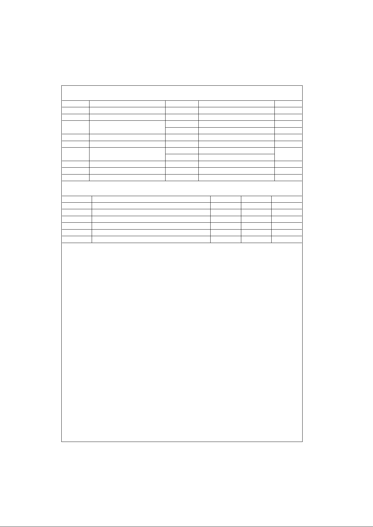
Absolute Maximum Ratings(Note 3)
Recommended Operating Conditions
Note 3: Absolute Maximum continuous ratings are those values beyond which damage to the device may occur. Exposure to these conditions or conditions
beyond those indica te d m ay adversely affect devic e reliability. Functional operation under absolute maximum rated conditions is not imp lied.
Note 4: I
O
Absolute Maximum Rating must be observed.
Symbol Parameter Value Conditions Units
V
CC
Supply Voltage −0.5 to +4.6 V
V
I
DC Input Voltage −0.5 to +7.0 V
V
O
DC Output Voltage −0.5 to +7.0 Output in 3-STATE V
−0.5 to +7.0 Output in HIGH or LOW State (Note 4) V
I
IK
DC Input Diode Current −50 VI < GND mA
I
OK
DC Output Diode Current −50 VO < GND mA
I
O
DC Output Current 64 VO > VCCOutput at HIGH State
mA
128 V
O
> VCCOutput at LOW State
I
CC
DC Supply Current per Supply Pin ±64 mA
I
GND
DC Ground Current per Ground Pin ±128 mA
T
STG
Storage Temperature −65 to +150 °C
Symbol Parameter Min Max Units
V
CC
Supply Voltage 2.7 3.6 V
V
I
Input Voltage 0 5.5 V
I
OH
HIGH-Level Output Current −32 mA
I
OL
LOW-Level Output Current 64 mA
T
A
Free-Air Operating Temperature −40 85 °C
∆t/∆V Input Edge Rate, V
IN
= 0.8V–2.0V, VCC = 3.0V 0 10 ns/V
 Loading...