

Fairchild Semiconductor 74ALVCR162601 Datasheet
September 2001
Revised October 2001
74ALVCR162601
Low Voltage 18-Bit Universal Bus Transceivers
with 3.6V Tolerant Inputs and Outputs
and 26
Ω Series Resistors in the Outputs
Series Resistors in the Outputs
74ALVCR162601 Low Voltage 18-Bit Universal Bus Transceivers with 3.6V Tolerant Inputs and Outputs and 26
General Description
The 74ALVCR162601, 18-bit universal bus transceiver,
combines D-type latches and D-type flip-flops to allow data
flow in transparent, latched, and clocked modes.
Data flow in each dir ection is controlled by output-enable
(OEAB
and OEBA), latch-enable (LEAB and LEBA), and
clock (CLKAB and CLKBA) inputs. The clock can be controlled by the clock-enable (CLKENAB
inputs. For A-to-B data flow, the device operates in the
transparent mode when LEAB is HIGH. When LEAB is
LOW, the A data is latched if CLKAB is held at a HIGH-toLOW logic level. If LEA B is LOW, the A bus data is s tored
in the latch/flip-flop on the LOW-to-HIGH transition of
CLKAB. Output-enable OEAB
is HIGH, the outputs ar e in the high-impedance state.
Data flow for B to A is similar to tha t of A to B but uses
OEBA
, LEBA, CLKBA and CLKENBA.
The 74ALVCR162601 is designed for low voltage (1.65V to
3.6V) V
The 74ALVCR162601 is also designed with 26
resistors on both the A and B Port ou tputs. This design
reduces line noise in applications such as memory address
drivers, clock drivers, and bus transceivers/transmitters.
applications with I/O compatibility up to 3.6V.
CC
is active-LOW. When OEAB
and CLKENBA)
Ω series
Features
■ 1.65–3.6V VCC supply operation
■ 3.6V tolerant inputs and outputs
■ 26
Ω series resistors on both the A and B Port outputs.
■ t
(A to B, B to A)
PD
4.3 ns max for 3.0V to 3.6V V
5.1 ns max for 2.3V to 2.7V V
9.2 ns max for 1.65V to 1.95V V
■ Power-down HIGH impedance inputs and outputs
■ Supports live insertion/withdrawal (Note 1)
■ Uses patented noise/EMI reductio n circuitr y
■ Latchup conforms to JEDEC JED78
■ ESD performance:
Human body model
Machine model
Note 1: To ensure the high-impedance state d uring power up or power
down, OE
should be tied to VCC through a pull-up r esistor; the min imum
value of the res istor is d eter mine d by the cu rre nt-sou rcin g ca pa bility of t he
driver.
>200V
CC
CC
CC
> 2000V
Ordering Code:
Order Number
74ALVCR162601T MTD56 56-Lead Thin Shrink Small Outline Package (TSSOP), JEDEC MO-153, 6.1mm Wide
Devices also availab l e in Tape and Reel. Specify by appending th e s uffix let t er “X” to the ordering code.
Package
Number
Package Description
© 2001 Fairchild Semiconductor Corporation DS500660 www.fairchildsemi.com
Ω
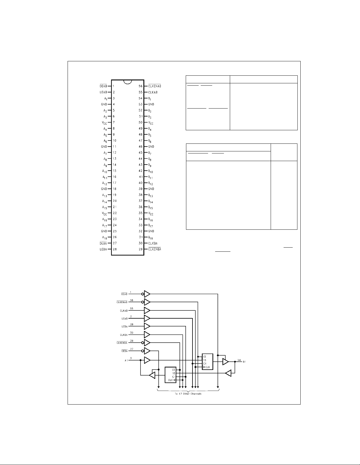
Connection Diagram Pin Descriptions
Pin Names Description
OEAB
, OEBA Output Enable Inputs (Active LOW)
LEAB, LEBA Latch Enable Inputs
CLKAB, CLKBA Clock Inputs
74ALVCR162601
CLKENAB
A
1–A18
B
1–B18
, CLKENBA Clock Enable Inputs
Side A Inputs or 3-STATE Outputs
Side B Inputs or 3-STATE Outputs
Logic Diagram
Function Table
(Note 2)
Inputs Outputs
CLKENAB
OEAB LEAB CLKAB A
B
n
n
XHXXXZ
XLHXLL
XLHXHH
HLLXXB
HLLXXB
LLL
LLL
↑ LL
↑ HH
LLLLXB
LLLHXB
H = HIGH Voltage Level
L = LOW Voltage Level
X = Immaterial (HIGH or LOW, inputs may not float)
Z = HIGH Impedance
Note 2: A-to-B data flow is shown; B-to-A flow is similar but uses OEBA
LEBA, CLKBA, and C LKENBA
Note 3: Output level be fore the indicated steady-s tate input conditions
were established
Note 4: Output level be fore the indicated steady-s tate input conditions
were established, pr ov ided that CL K AB was HIGH be f o re LEAB went LOW.
.
(Note 3)
0
(Note 3)
0
(Note 3)
0
(Note 4)
0
,
www.fairchildsemi.com 2
 Loading...