

Fairchild Semiconductor 74ALVCH2245 Datasheet
January 2002
Revised January 2002
74ALVCH2245
Low Voltage Bidirectional Transceiver with Bushold
74ALVCH2245 Low Voltage Bidirectional Transceiver with Bushold
and 26
General Description
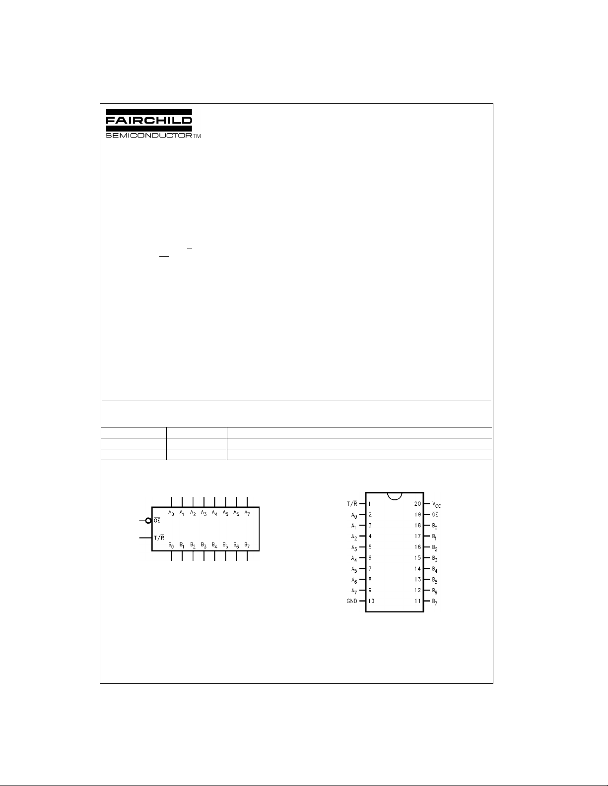
The ALVCH2245 contains eight non-inverting bidirectional
buffers with 3-STATE outputs and is in tended for bus oriented applications . The T/R
of data flow. The OE
by placing them in a high impedance state. The
ALVCH2245 data inputs include active bushold circuitry,
eliminating the need fo r external pull-up resistors to hold
unused or floating data inputs at a valid logic level.
The 74ALVCH2245 is designed for low vol tage (1.65V to
3.6V) V
with 26
design reduces line n oise in applicatio ns such as memo ry
address drivers, clock dr ivers, and b us transceivers t ransmitters
The 74ALVCH2245 is fabricated with an advanced C MOS
technology to achieve high-speed operation while maintaining low CMOS power dissipation.
Ω Series Resistors in B Outputs
Features
■ 1.65V to 3.6V VCC supply operation
input determines the direction
input disables b oth th e A and B P o rts
applications. The ALVCH2245 is also designed
CC
Ω series resistance in the B Port outputs. This
■ 3.6V tolerant control inputs
■ Bushold on data inputs eliminates the need for external
pull-up/pull-down resistors
■ 26
■ t
PD
4.9 ns max for 3.0V to 3.6V V
6.1 ns max for 2.3V to 2.7V V
9.8 ns max for 1.65V to 1.95V V
■ Uses patented Quiet Series noise/EMI reduction
circuitry
■ Latchup conforms to JEDEC JED78
■ ESD performance:
Human body model
Machine model
Ω series resistors in B Port outputs
(A to B)
CC
CC
CC
> 2000V
> 200V
Ordering Code:
Order Number Package Number Package Description
74ALVCH2245WM M20B 20-Lead Small Outline Integrated Circuit (SOIC), JEDEC MS-013, 0.300" Wide
74ALVCH2245MTC MTC20 20-Lead Thin Shrink Small Outline Package (TSSOP), JEDEC MO-153, 4.4mm Wide
Devices also availab le in Tape and Reel. Specify by appending the suffix letter “X” to the o rdering code.
Logic Symbol Connection Diagram
Quiet Series is a tra demark of Fairchild Semiconductor Corp oration.
© 2002 Fairchild Semiconductor Corporation ds500716 www.fairchildsemi.com
Pin Descriptions Truth Table
Pin Names Description
OE
T/R
74ALVCH2245
A
0–A7
B
0–B7
Output Enable Input (Active LOW)
Transmit/Receive Input
Side A Bushold Inputs or 3-STATE Outputs
Side B Bushold Inputs or 3-STATE Outputs
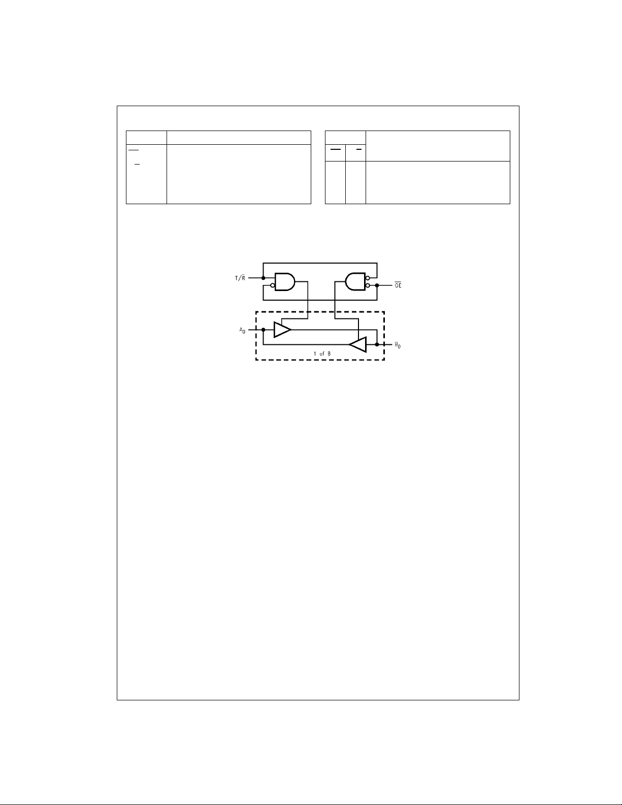
Logic Diagram
Inputs
Outputs
OE
T/R
L L Bus B0–B7 Data to Bus A0–A
L H Bus A0–A7 Data to Bus B0–B
H X HIGH Z State on A0–A7, B0–B7
H = HIGH Voltage Level
L = LOW Voltage Level
X = Immaterial
Z = High Impedance
7
7
www.fairchildsemi.com 2
Absolute Maximum Ratings(Note 1) Recommended Operating
Supply Voltage (VCC) −0.5V to +4.6V
DC Input Voltage (V
Output Voltage (V
DC Input Diode Current (I
V
< 0V −50 mA
I
DC Output Diode Current (I
< 0V −50 mA
V
O
) −0.5V to 4.6V
I
) (Note 2) −0.5V to VCC +0.5V
O
)
IK
)
OK
DC Output Source/Sink Current
(I
) ±50 mA
OH/IOL
or GND Current per
DC V
CC
Supply Pin (I
Storage Temperature Range (T
or GND) ±100 mA
CC
) −65°C to +150°C
STG
Conditions
Power Supply
Operating 1.65V to 3.6V
Input Voltage 0V to V
Output Voltage (VO)0V to V
Free Air Operating Temperature (TA) −40°C to +85°C
Minimum Input Edge Rate (
= 0.8V to 2.0V, VCC = 3.0V 10 ns/V
V
IN
Note 1: The Absolute Maxi mum Ratings are thos e values beyond which
the safety of the d evice cannot b e guaranteed . The device sh ould not be
operated at these limit s. The parametric values defi ned in the Electrical
Characteristics tables are not guaranteed at the Absolute Maximum Ratings. The “Recommended Operating Conditions” table will define the conditions for actual device operation.
Absolute Maximum Rating must be observed.
Note 2: I
O
Note 3: Floating or unused control inputs must be held HIGH or LOW.
(Note 3)
∆t/∆V)
DC Electrical Characteristics
V
Symbol Parameter Conditions
V
V
V
V
I
I
HIGH Level Input Voltage 1.65 - 1.95 0.65 x V
IH
LOW Level Input Voltage 1.65 - 1.95 0.35 x V
IL
HIGH Level Output Voltage IOH = −100 µA 1.65 - 3.6 VCC - 0.2
OH
A Outputs IOH = −4 mA 1.65 1.2
HIGH Level Output Voltage IOH = −100 µA 1.65 - 3.6 VCC - 0.2
B Outputs I
LOW Level Output Voltage IOL = 100 µA 1.65 - 3.6 0.2
OL
A Outputs IOL = 4 mA 1.65 0.45
LOW Level Output Voltage IOL = 100 µA 1.65 - 3.6 0.2
B Outputs IOL = 2 mA 1.65 0.45
Input Leakage Current 0 ≤ VI ≤ 3.6V 1.65 - 3.6 ±5.0 µA
I
= −6 mA 2.3 2.0
OH
= −12 mA 2.3 1.7
I
OH
IOH = −24 mA 3.0 2
= −2 mA 1.65 1.2
OH
= −4 mA 2.3 1.9
I
OH
IOH = −6 mA 2.3 1.7
IOH = −8 mA 2.7 2
IOH = −12 mA 3.0 2
IOL = 6 mA 2.3 0.4
IOL = 12 mA 2.3 0.7
IOL = 24 mA 3.0 0.55
IOL = 4 mA 2.3 0.4
IOL = 6 mA 2.3 0.55
IOL = 8 mA 2.7 0.6
IOL = 12 mA 3.0 0.8
CC
(V)
2.7 - 3.6 2.0
2.7 - 3.6 0.8
2.7 2.2
3.0 2.4
3.0 2.4
2.7 0.4
3.0 0.55
Min Max Units
CC
74ALVCH2245
CC
CC
V2.3 - 2.7 1.7
CC
V2.3 - 2.7 0.7
V
V
3 www.fairchildsemi.com
 Loading...