

Fairchild Semiconductor 74ALVCH16373 Datasheet
October 2001
Revised February 2002
74ALVCH16373
Low Voltage 16-Bit Transparent Latch with Bushold
74ALVCH16373 Low Voltage 16-Bit Transparent Latch with Bushold
General Description
The ALVCH16373 contains sixteen non-inverting latches
with 3-STATE outputs and is intended for bus oriented
applications. The device is byte controlled. The flip-flops
appear to be transparent to the data when the Latch
Enable (LE) is HIGH. When LE is LOW, the data that meets
the setup time is l atched. Data appe ars on the bus wh en
the Output Enable (OE
outputs are in a high impedance state.
The ALVCH16373 data inputs include acti ve bushold circuitry, eliminating the need for external pull-up resistors to
hold unused or floating data inputs at a valid logic level.
The 74ALVCH16373 is designed for low volta ge (1.65V to
3.6V) V
The 74ALVCH16373 is fabricated with an advanced CMOS
technology to achieve high speed operation while maintaining low CMOS power dissipation.
applications with output compatibility up to 3.6V.
CC
) is LOW. When OE is HIGH, the
Features
■ 1.65V to 3.6V VCC supply operation
■ 3.6V tolerant control inputs and outputs
■ Bushold on data inputs eliminates the need for external
pull-up/pull-down resistors
■ t
(In to On)
PD
3.6 ns max for 3.0V to 3.6V V
4.5 ns max for 2.3V to 2.7V V
6.8 ns max for 1.65V to 1.95V V
■ Uses patented noise/EMI reductio n circuitr y
■ Latch-up conforms to JEDEC JED78
■ ESD performance:
Human body model
Machine model
> 200V
CC
CC
CC
> 2000V
Ordering Code:
Order Number
74ALVCH16373T MTD48 48-Lead Thin Shrink Small Outline Package (TSSOP), JEDEC MO-153, 6.1mm Wide
Devices also availab l e in Tape and Reel. Specify by appending su ffix let te r “X” to the ordering code.
Package
Number
Package Description
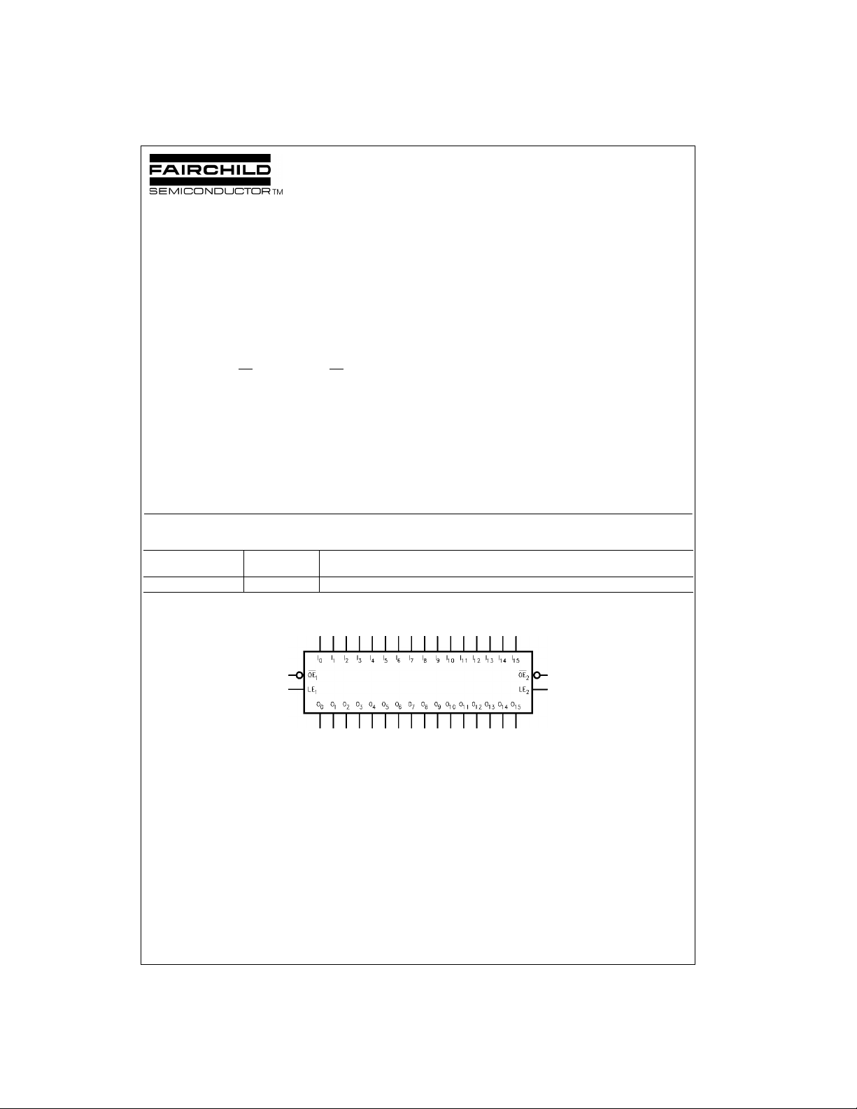
Logic Symbol
© 2002 Fairchild Semiconductor Corporation DS500631 www.fairchildsemi.com
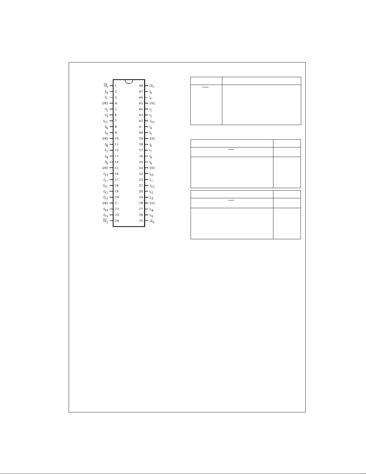
Connection Diagram Pin Descriptions
Pin Names Description
OE
n
LE
n
I
74ALVCH16373
O
0–I15
0–O15
NC No Connect
Truth Tables
LE
1
XHXZ
HLLL
HLHH
LLXO
LE
2
XHXZ
HLLL
HLHH
LLXO
H = HIGH Voltage Level
L = LOW Voltage Level
X = Immaterial (HIGH or LOW, control inputs may not float)
Z = High Impedance
= Previous O0 before HIGH-to-LOW of Latch Enable
O
0
Output Enable Input (Active LOW)
Latch Enable Input
Bushold Inputs
Outputs
Inputs Outputs
OE
1
I0–I
7
O0–O
0
Inputs Outputs
OE
2
I8–I
15
O8–O
0
7
15
www.fairchildsemi.com 2
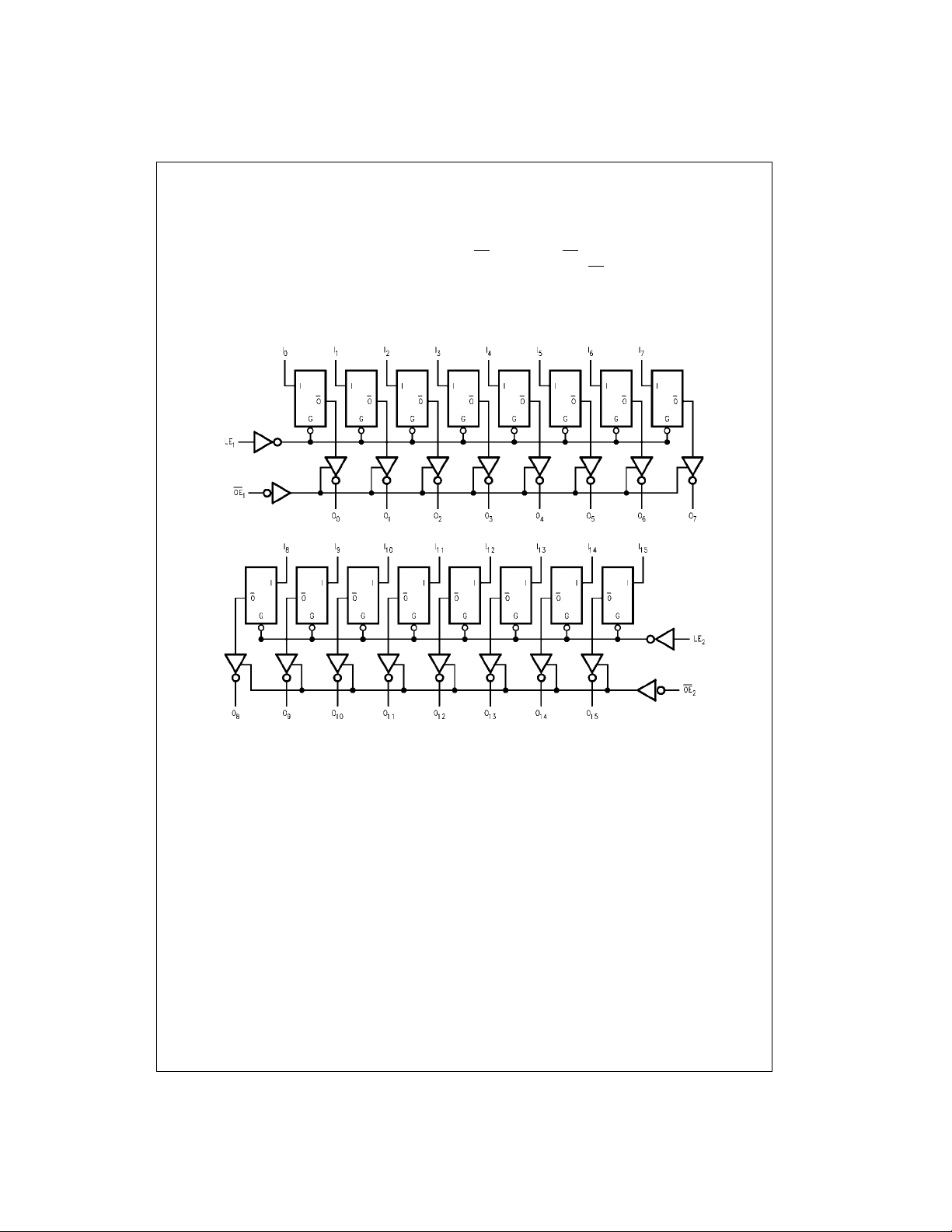
Functional Description
The 74ALVCH16373 contains sixteen edge D-type latches
with 3-STATE outputs. The dev ice is byte controlled with
each byte functioning identically, but independent of the
other. Control pins can be sh orted together to obtain full
16-bit operation. The foll owing description ap plies to each
byte. When the Latch Enable (LE
enters the latches. In this condit ion the latches are
the I
n
transparent, i.e., a latch output will change state each time
) input is HIGH, data on
n
Logic Diagram
its I input changes. When LE
information that was present on the I inputs a setup time
preceding the HIGH-to-LOW transition on LE
3-STATE outputs are controlled by the Output Enable
(OE
) input. When OEn is LOW the standard outputs are in
n
the 2-state mode. When OE
are in the high i mp eda nce m ode bu t th i s d oes no t i nt erf ere
with entering new data into the latches.
is LOW, the latches store
n
. The
n
is HIGH, the standard outputs
n
74ALVCH16373
Please note that this diagram is provided only for the understanding of logic operations and should not be used to estimate propagation delays.
3 www.fairchildsemi.com
 Loading...