

Fairchild Semiconductor 74ACTQ827SPC, 74ACTQ827SCX, 74ACTQ827SC, 74ACTQ827CW Datasheet
March 1990
Revised December 1998
74ACTQ827 Quiet Series 10-Bit Buffer/Li ne Driver with 3-STATE Outputs
© 1999 Fairchild Semiconductor Corporation DS010687.prf www.fairchildsemi.com
74ACTQ827
Quiet Series 10-Bit Buffer/Line Driver
with 3-STATE Outputs
General Description
The ACTQ827 10-bit bus buffer provides high per for man ce
bus interface buffering for wide data/address paths or
buses carrying parity. The 10-bit buffers have NOR output
enables for maximum control flexibility. The ACTQ827 utilizes Fairchild Quiet Series technology to guarantee quiet
output switching and improved dynam ic threshold performance. FACT Quiet Series features G TO output control
and undershoot correct or in addition t o a split ground bus
for superior performance.
Features
■ Guaranteed simultaneous switching noise level and
dynamic threshold performance
■ Guaranteed pin-to-pin skew AC performance
■ Inputs and outputs on opposit e sides of package allow
easy interface with microprocessors
■ Improved latch-up immunity
■ Outputs source/sink 24 mA
■ Functionally and pin-compatible to AMD’s AM29827
■ Has TTL-com patible inputs
Ordering Code:
Device also available in Tape and Reel. Specify by appendin g s uf f ix let t er “X” to the ordering co de.
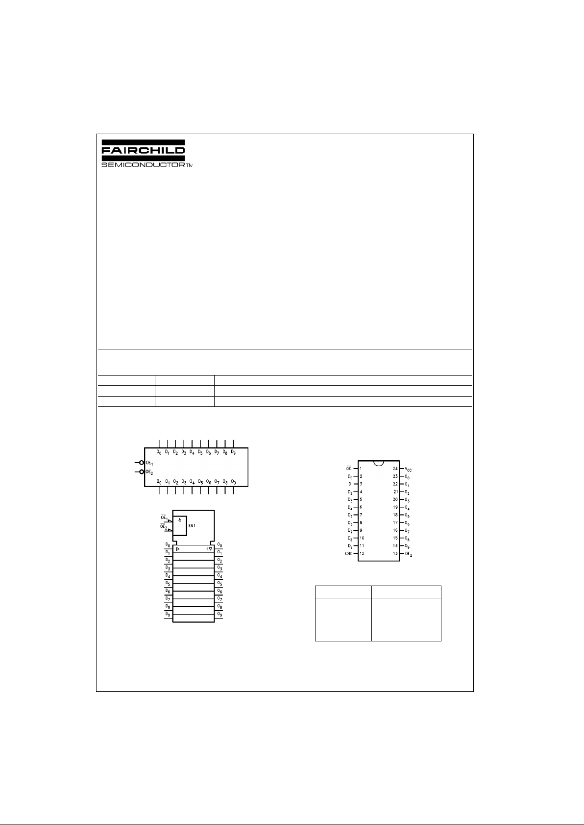
Logic Symbols
IEEE/IEC
Connection Diagram
Pin Assignment
for DIP and SOIC
Pin Descriptions
FACT, Quiet Series, FACT Quiet Series and GTO are trademarks of Fairchild Semiconductor Co rporation.
Order Number Package Number Package Description
74ACTQ827SC M24B 24-Lead Small Outline Integrated Circuit (SOIC), JEDEC MS-013, 0.300” Wide Body
74ACTQ827SPC N24C 24-Lead Plastic Dual-In-Line Package (PDIP), JEDEC MS-100, 0.300” Wide
Pin Names Description
OE
1
, OE
2
Output Enable
D
0–D9
Data Inputs
O
0–O9
Data Outputs
www.fairchildsemi.com 2
74ACTQ827
Functional Description
The ACTQ827 line driver is designed to be employed as
memory address driver, clock driver and bus-oriented
transmitter/receiver. The devices have 3-STATE outputs
controlled by the Output Enable (OE
) pins. When the OE is
LOW, the device is transparent. When OE
is HIGH, the
device is in 3-STATE mode.
Function Table
H = HIGH Voltage Level
L = LOW Voltage Level
Z = HIGH Impedance
X = Immaterial
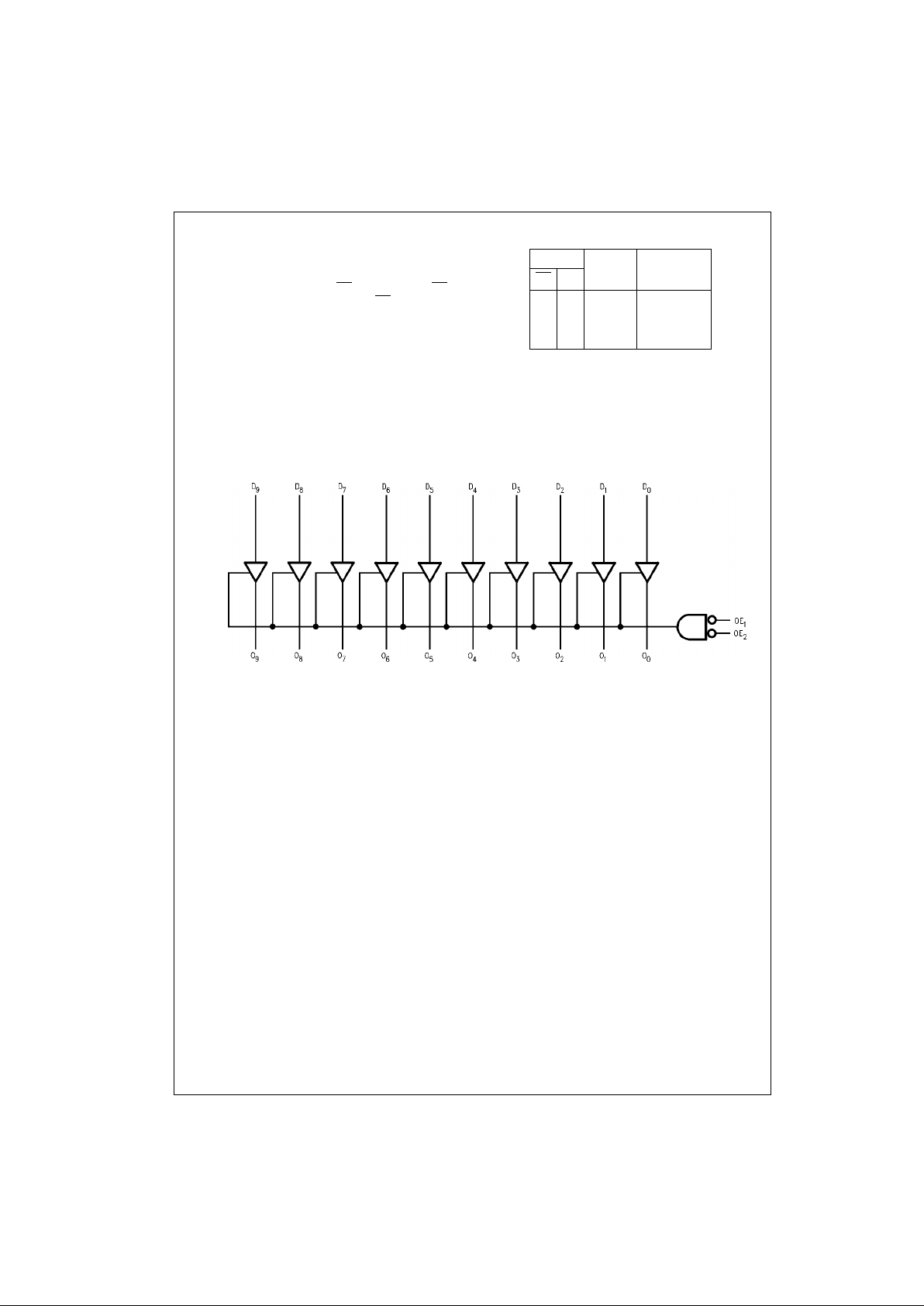
Logic Diagram
Please note that this diagram is provided only for the understanding of logic operations and should not be used to estimate p ropagation delays.
Inputs Outputs Function
OE
D
n
O
n
L H H Transparent
L L L Transparent
H X Z High Z
3 www.fairchildsemi.com
74ACTQ827
Absolute Maximum Ratings(Note 1)
Recommended Operating
Conditions
Note 1: Absolute maximum ratings are those values beyond which damage
to the device may occur. The databook specifications should be met, without exception, to ensure that the system design is reliable over its power
supply, temperature, and output/in put loading variables. Fairchild does n ot
recommend operat ion of FACT circuits outside databook specifications.
DC Electrical Characteristic
Supply Voltage (VCC) −0.5V to +7.0V
DC Input Diode Current (I
IK
)
V
I
= −0.5V −20 mA
V
I
= VCC + 0.5V +20 mA
DC Input Voltage (V
I
) −0.5V to VCC + 0.5V
DC Output Diode Current (I
OK
)
V
O
= −0.5V −20 mA
V
O
= VCC + 0.5V +20 mA
DC Output Voltage (V
O
) −0.5V to VCC + 0.5V
DC Output Source
or Sink Current (I
O
) ± 50 mA
DC V
CC
or Ground Current
per Output Pin (I
CC
or I
GND
) ± 50 mA
Storage Temperature (T
STG
) −65°C to +150°C
DC Latch-Up Source
or Sink Current ± 300 mA
Junction Temperature (T
J
)
PDIP 140°C
Supply Voltage (V
CC
) 4.5V to 5.5V
Input Voltage (V
I
)0V to V
CC
Output Voltage (VO)0V to V
CC
Operating Temperature (TA) −40°C to +85°C
Minimum Input Edge Rate ∆V/∆t 125 mV/ns
V
IN
from 0.8V to 2.0V
V
CC
@ 4.5V, 5.5V
Symbol Parameter
V
CC
TA = +25°CT
A
= −40°C to +85°C
Units Conditions
(V) Typ Guaranteed Limits
V
IH
Minimum HIGH Level 4.5 1.5 2.0 2.0 V V
OUT
= 0.1V
Input Voltage 5.5 1.5 2.0 2.0 or VCC − 0.1V
V
IL
Maximum LOW Level 4.5 1.5 0.8 0.8 V V
OUT
= 0.1V
Input Voltage 5.5 1.5 0.8 0.8 or VCC − 0.1V
V
OH
Minimum HIGH Level 4.5 4.49 4.4 4.4 V I
OUT
= −50 µA
Output Voltage 5.5 5.49 5.4 5.4
VIN = VIL or V
IH
4.5 3.86 3.76 V IOH = −24 mA
5.5 4.86 4.76 IOH = −24 mA (Note 2)
V
OL
Maximum LOW Level 4.5 0.001 0.1 0.1 V I
OUT
= 50 µA
Output Voltage 5.5 0.001 0.1 0.1
VIN = VIL or V
IH
4.5 0.36 0.44 V IOL = 24 mA
5.5 0.36 0.44 IOL = 24 mA (Note 2)
I
IN
Maximum Input 5.5 ±0.1 ±1.0 µAVI = VCC, GND
Leakage Current
I
OZ
Maximum 3-STATE 5.5 ±0.5 ±5.0 µAVI = VIL, V
IH
Current VO = VCC, GND
I
CCT
Maximum ICC/Input 5.5 0.6 1.5 mA VI = VCC − 2.1V
I
OLD
Minimum Dynamic 5.5 75 mA V
OLD
= 1.65V Max
I
OHD
Output Current (Note 3) 5.5 −75 mA V
OHD
= 3.85V Min
I
CC
Maximum Quiescent 5.5 8.0 80.0 µAVIN = V
CC
Supply Current or GND
V
OLP
Quiet Output 5.0 1.1 1.6V V Figure 1, Figure 2
Maximum Dynamic V
OL
(Note 4)(Note 5)
V
OLV
Quiet Output 5.0 −0.6 −1.3 V Figure 1, Figure 2
Minimum Dynamic V
OL
(Note 4)(Note 5)
V
IHD
Minimum HIGH Level 5.0 1.9 2.0 V (Note 4)(Note 6)
Dynamic Input Voltage
V
ILD
Maximum LOW Level 5.0 1.2 0.8 V (Note 4)(Note 6)
Dynamic Input Voltage
 Loading...