

Fairchild Semiconductor 74ACTQ823SPC, 74ACTQ823SCX, 74ACTQ823SC, 74ACTQ823CW Datasheet
May 1991
Revised December 1998
74ACTQ823 Quiet Series 9-Bit D-Type Flip-Flop with 3-STATE Outputs
© 1999 Fairchild Semiconductor Corporation DS010921.prf www.fairchildsemi.com
74ACTQ823
Quiet Series 9-Bit D-Type Flip-Flop
with 3-STATE Outputs
General Description
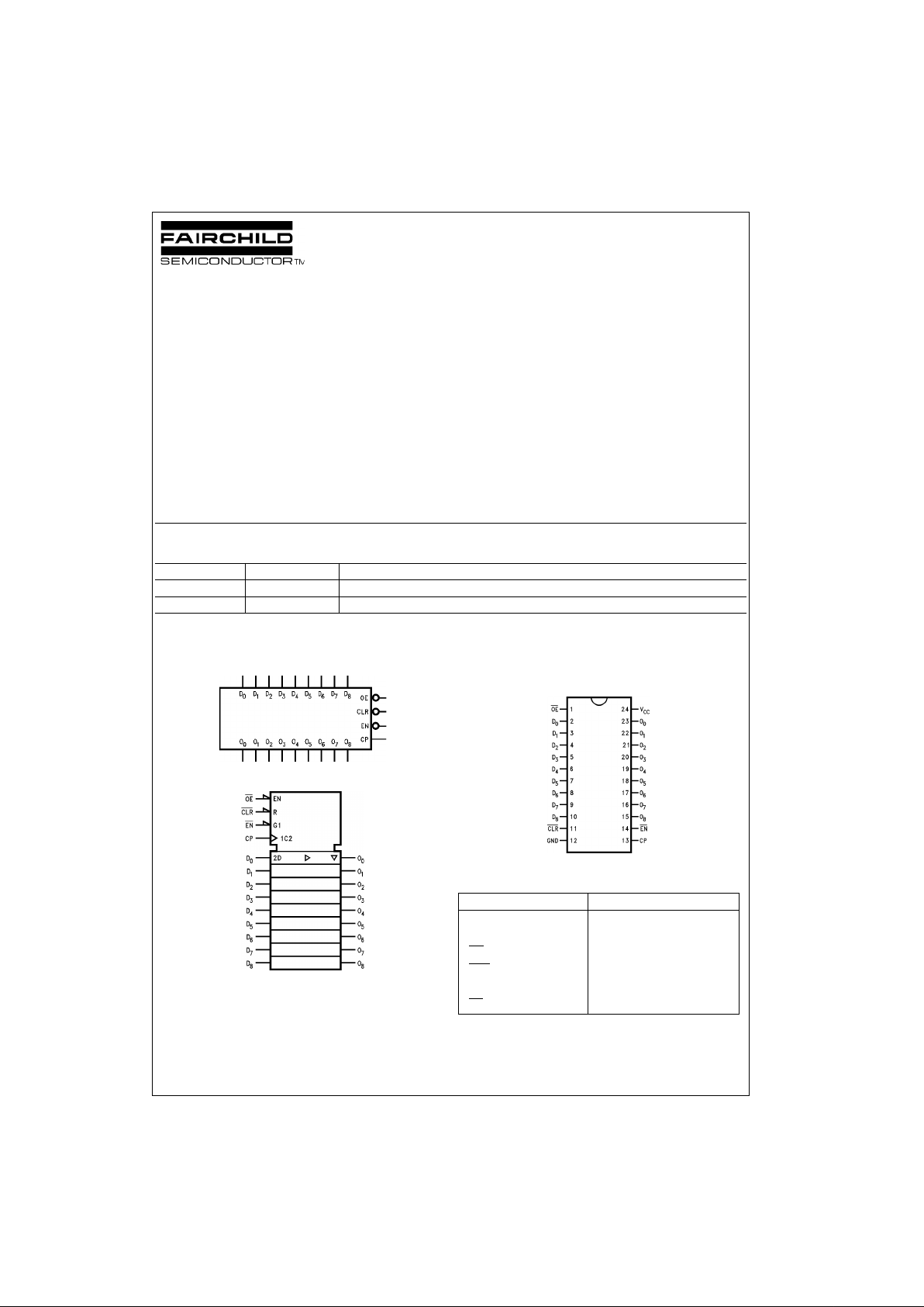
The ACTQ823 is a 9-bit buffered register. It features Clock
Enable and Clear which are ideal for parity bus interfacing
in high performance microprogramming systems. The
ACTQ823 utilizes Fairchild Quiet Series technology to
guarantee quiet output switching and improved dynamic
threshold performance. FACT Quiet Series features
GTO output control and und ershoot c orrector in a ddition
to a split ground bus for superior performance.
Features
■ Guaranteed simultaneous switching noise level and
dynamic threshold performance
■ Guaranteed pin-to-pin skew AC performance
■ Inputs and outputs on opposit e sides of package allow
easy interface with microprocessors
■ Improved latch-up immunity
■ Has TTL-com patible inputs
Ordering Code:
Device also available in Tape and Reel. Specify by appendin g s uf f ix let t er “X” to the ordering for m .
Logic Symbols
IEEE/IEC
Connection Diagram
Pin Assignment
for DIP and SOIC
Pin Descriptions
FACT, Quiet Series, FACT Quiet Series and GTO are trademarks of Fairchild Semiconductor Co rporation.
Order Number Package Number Package Description
74ACTQ823SC M24B 24-Lead Small Outline Integrated Circuit (SOIC), JEDEC MS-013, 0.300” Wide Body
74ACTQ823SPC N24C 24-Lead Plastic Dual-In-Line Package (PDIP), JEDEC MS-100, 0.300” Wide
Pin Names Description
D
0–D8
Data Inputs
O
0–O8
Data Outputs
OE
Output Enable
CLR
Clear
CP Clock Input
EN
Clock Enable
www.fairchildsemi.com 2
74ACTQ823
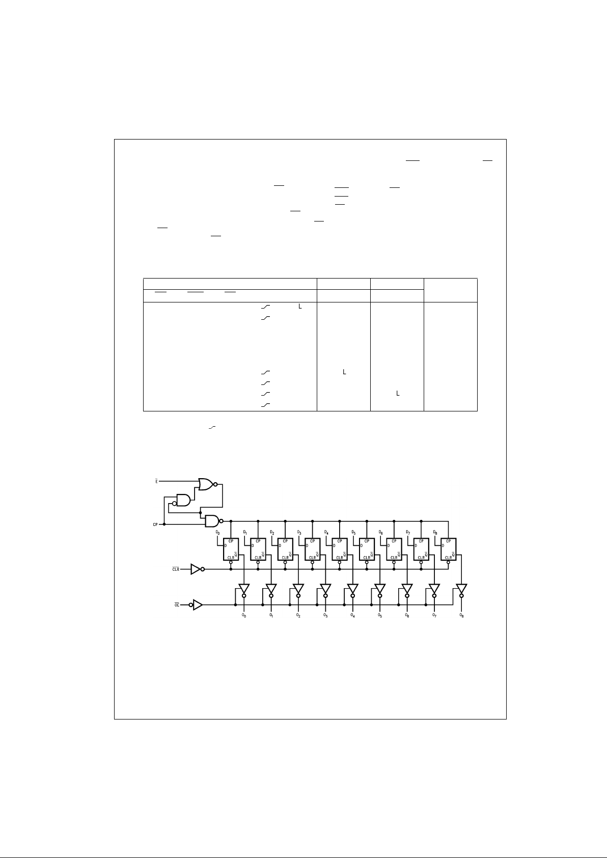
Functional Description
The ACTQ823 consists of nin e D-type edge-trig gered flipflops. These have 3-STATE outputs for bus systems organized with inputs and outputs on opposite sides. The buffered clock (CP) and buffered Output Enable (OE
) are
common to all flip- flop s. The fli p-f lops w ill stor e th e st ate of
their individual D input s that m eet the setup and hold tim e
requirements on th e LOW-to-HIGH CP trans ition. Wi th OE
LOW, the contents of the flip-flop s are available at th e ou tputs. When OE
is HIGH, the outputs go to t he high im ped-
ance state. Operation of the OE
input does not af fect the
state of the flip-flo ps. In addition to the Clock and Outp ut
Enable pins, there are Clea r (CLR
) and Clock Enable (EN)
pins. These devices are ideal for parit y bus interfacing in
high performance systems.
When CLR
is LOW and OE is LOW, the outputs are LOW.
When CLR
is HIGH, data can be entered into the flip-flops.
When EN
is LOW, data on the inputs is transferred to the
outputs on the LOW-to-HIGH clock transition. When the
EN
is HIGH, the outputs do not change state, regardless of
the data or clock input transitions.
Function Table
H = HIGH Voltage Level Z = High Imped ance
L = LOW V oltage Level
= LOW-to-HIGH Transition
X = Immaterial NC = No Change
Logic Diagram
Please note that this diagram is provided only for the understanding of logic operations and should not be used to estimat e propagation delays.
Inputs Internal Output Function
OE
CLR EN CP D Q O
H X L
L L Z High Z
H X L
H H Z High Z
H L X X X L Z Clear
L L X X X L L Clear
H H H X X NC Z Hold
L H H X X NC NC Hold
H H L
L L Z Load
H H L
H H Z Load
L H L
L L L Load
L H L
H H H Load
3 www.fairchildsemi.com
74ACTQ823
Absolute Maximum Ratings(Note 1)
Recommended Operating
Conditions
Note 1: Absolute maximum ratings are thos e values beyond which dam-
age to the device may occur. The databook specifications should be met,
without exception, to ensure that the system design is reliable over its
power supply, temperature, and output/in put loading variables. Fairchild
does not recommend operation of FACT circuits outside databook specifications.
DC Electrical Characteristics for ACTQ
Note 2: All outputs loaded; thresholds on input associated with ou t put under test.
Note 3: Maximum test duration 2.0 ms, one output loaded at a time.
Note 4: Maximum test duration 2.0 ms, one output loaded at a time.
Note 5: PDIP package.
Note 6: Max number of ou t puts defined as (n). Data inputs are driven 0V to 3V. One output @ GND.
Supply Voltage (VCC) −0.5V to +7.0V
DC Input Diode Current (I
IK
)
V
I
= −0.5V −20 mA
V
I
= VCC + 0.5V +20 mA
DC Input Voltage (V
I
) −0.5V to VCC + 0.5V
DC Output Diode Current (I
OK
)
V
O
= −0.5V −20 mA
V
O
= VCC + 0.5V +20 mA
DC Output Voltage (V
O
) −0.5V to VCC + 0.5V
DC Output Source
or Sink Current (I
O
) ± 50 mA
DC V
CC
or Ground Current
per Output Pin (I
CC
or I
GND
) ± 50 mA
Storage Temperature (T
STG
) −65°C to +150°C
DC Latch-Up Source
or Sink Current ± 300 mA
Junction Temperature (T
J
)
PDIP 140°C
Supply Voltage (V
CC
) 4.5V to 5.5V
Input Voltage (V
I
) 0V to V
CC
Output Voltage (VO) 0V to V
CC
Operating Temperature (TA) −40°C to +85°C
Minimum Input Edge Rate ∆V/∆t 125 mV/ns
V
IN
from 0.8V to 2.0V
V
CC
@ 4.5V, 5.5V
Symbol Parameter
V
CC
TA = +25°C TA = −40°C to +85°C
Units Conditions
(V) Typ Guaranteed Limits
V
IH
Minimum HIGH Level Input Voltage 4.5 1.5 2.0 2.0 V V
OUT
= 0.1V
5.5 1.5 2.0 2.0 or VCC − 0.1V
V
IL
Maximum LOW Level 4.5 1.5 0.8 0.8 V V
OUT
= 0.1V
Input Voltage 5.5 1.5 0.8 0.8 or VCC − 0.1V
V
OH
Minimum HIGH Level 4.5 4.49 4.4 4.4 V I
OUT
= −50 µA
Output Voltage 5.5 5.49 5.4 5.4
VIN = VILor V
IH
4.5 3.86 3.76 V IOH = −24 mA
5.5 4.86 4.76 IOH = −24 mA (Note 2)
V
OL
Maximum LOW Level 4.5 0.001 0.1 0.1 V I
OUT
= 50 µA
Output Voltage 5.5 0.001 0.1 0.1
VIN = VILor V
IH
4.5 0.36 0.44 V IOL = 24 mA
5.5 0.36 0.44 IOL = 24 mA (Note 2)
I
IN
Maximum Input Leakage Current 5.5 ± 0.1 ± 1.0 µAVI = VCC, GND
I
OZ
Maximum 3-STATE 5.5 ± 0.5 ± 5.0 µAVI = VIL, V
IH
Leakage Current VO = VCC, GND
CCT
Maximum ICC/Input 5.5 0.6 1.5 mA VI = VCC − 2.1V
OLD
Minimum Dynamic 5.5 75 mA V
OLD
= 1.65V Max
I
OHD
Output Current (Note 2) 5.5 −75 mA V
OHD
= 3.85V Min
I
CC
Maximum Quiescent Supply Current 5.5 8.0 80.0 µAVIN = VCC or GND
V
OLP
Quiet Output 5.0 1.1 1.5 V Figure 1, Figure 2
Maximum Dynamic V
OL
(Note 5)(Note 6)
V
OLV
Quiet Output 5.0 −0.6 −1.2 V Figure 1, Figure 2
Minimum Dynamic V
OL
(Note 5)(Note 6)
V
IHD
Minimum HIGH Level Dynamic Input Voltage 5.0 1.9 2.2 V (Note 5)(Note 7)
V
ILD
Maximum LOW Level Dynamic Input Voltage 5.0 1.2 0.8 V (Note 5)(Note 7)
 Loading...