

Fairchild Semiconductor 74ABT244CSJX, 74ABT244CSJ, 74ABT244CSCX, 74ABT244CSC, 74ABT244CPC Datasheet
...
May 1992
Revised November 1999
74ABT244
Octal Buffer/Line Driv e r with 3-STATE Outputs
74ABT244 Octal Buffer/Line Driver with 3-STATE Outputs
General Description
The ABT244 is an octal buffer and line driver with 3-STATE
outputs designed to be employed as a memory and
address driver, clock driver, or bus-oriented transmitter/
receiver.
Features
■ Non-inverting buffers
■ Output sink capability of 64 mA, source capability of
32 mA
■ Guaranteed output skew
■ Guaranteed multiple output switching specifications
■ Output switching sp ecified for both 50 pF and 250 pF
loads
■ Guaranteed simultaneous switching, noise level and
dynamic threshold performan ce
■ Guaranteed latchup protection
■ High impedance glitch free bus loading during entire
power up and power down cycle
■ Nondestructive hot insertion capability
■ Disable time less than ena ble time to avoi d bus conten-
tion
Ordering Code:
Order Number Package Number Package Description
74ABT244CSC M20B 20-Lead Small Outline Integrated Circuit (SOIC), JEDEC MS-013, 0.300” Wide Body
74ABT244CSJ M20D 20-Lead Small Outline Package (SOP), EIAJ TYPE II, 5.3mm Wide
74ABT244CMSA MSA20 20-Lead Shrink Small Outline Package (SSOP), EIAJ TYPE II, 5.3mm Wide
74ABT244CMTC MTC20 20-Lead Thin Shrink Small Outline Package (TSSOP), JEDEC MO-153, 4.4mm Wide
74ABT244CPC N20A 20-Lead Plastic Dual-In-Line Package (PDIP), JEDEC MS-001, 0.300” Wide
Device also available in Tape and Reel. Specify by appending suffix letter “X” to the or dering code.
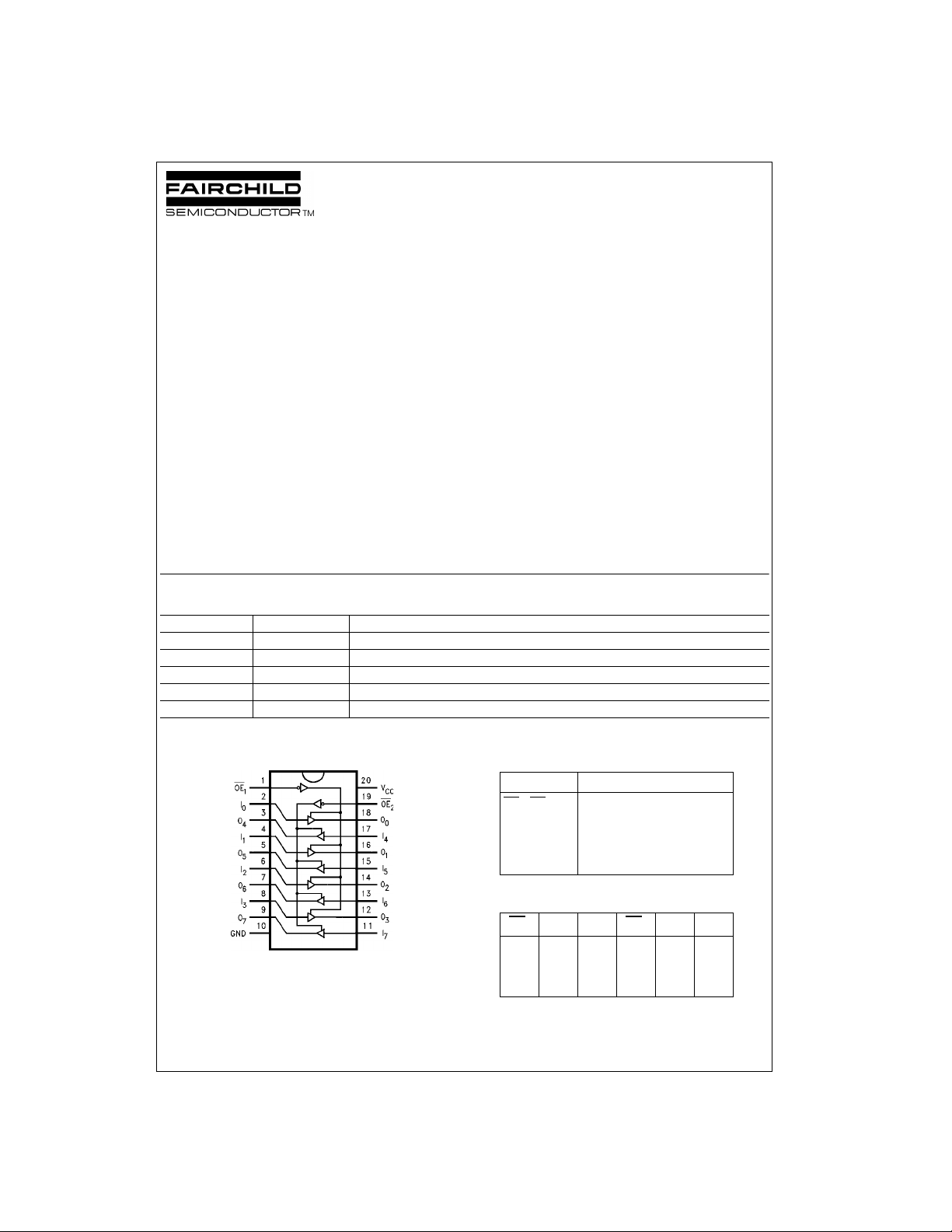
Connection Diagram Pin Descriptions
Pin Names Description
OE
I
0–I7
O
1
0–O7
, OE
Output Enable Input
2
(Active LOW)
Inputs
Outputs
Truth Table
OE
1I0–3O0–3
HXZHXZ
LHHLHH
LLLLLL
H = HIGH Voltage Level
L = LOW Voltage Level
X = Immaterial
Z = High Impedance
© 1999 Fairchild Semiconductor Corporation DS010992 www.fairchildsemi.com
OE2I
4–7O4–7
Absolute Maximum Ratings(Note 1) Recommended Operating
Storage Temperatur e −65°C to +150°C
Ambient Temperature under Bias −55°C to +125°C
74ABT244
Junction Temperature under Bias −55°C to +150°C
V
Pin Potential to Ground Pin −0.5V to +7.0V
CC
Input Voltage (Note 2) −0.5V to +7.0V
Input Cur rent (Note 2) −30 mA to +5.0 mA
Voltage Applied to Any Output
in the Disabled or
Power-Off State −0.5V to 5.5V
in the HIGH State −0.5V to V
Current Applied to Output
in LOW State (Max) twice th erated I
DC Latchup Source Current −5 00 mA
Over Voltage Latchup (I/O) 10V
OL
Conditions
Free Air Ambient Temperature −40°C to +85°C
Supply Voltage +4.5V to +5.5V
Minimum Input Edge Rate (∆V/∆t)
Data Input 50 mV/ns
Enable Input 20 mV/ns
CC
(mA)
Note 1: Absolute maximum ratings are values beyond which the device
may be damaged or have its useful life impair ed. Functional operation
under these conditi ons is not implied.
Note 2: Either voltage lim it or c urrent limit is sufficient to prot ect inputs.
DC Electrical Characteristics
Symbol Parameter Min Typ Max Units
V
Input HIGH Voltage 2.0 V Recognized HIGH Signal
IH
V
Input LOW Voltage 0.8 V Recognized LOW Signal
IL
V
Input Clamp Diode Voltage −1.2 V Min IIN = −18 mA
CD
V
Output HIGHVoltage 2.5 V Min IOH = −3 mA
OH
2.0 V Min IOH = −32 mA
V
Output LOWVoltage 0.55 IOL = 64 mA
OL
I
Input HIGH Current 1 µAMaxVIN = 2.7V (Note 4)
IH
1V
I
Input HIGH Current Breakdown Test 7 µAMaxVIN = 7.0V
BVI
I
Input LOW Current −1
IL
−1V
V
Input Leakage Test 4.75 V 0.0 IID = 1.9 µA
ID
I
Output Leakage Current 10 µA0 − 5.5V
OZH
I
Output Leakage Current −10 µA0 − 5.5V
OZL
I
Output Short-Circuit Current −100 −275 mA Max V
OS
I
Output High Leakage Current 50 µAMaxV
CEX
I
Bus Drainage Test 100 µA0.0V
ZZ
I
Power Supply Current 50 µA Max All Outputs HIGH
CCH
I
Power Supply Current 30 mA Max All Outputs LOW
CCL
I
I
Power Supply Current
CCZ
Additional ICC/Input Outputs Enabled 2.5 mA
CCT
50 µAMax
Outputs 3-STATE 2.5 mA Enable Input VI = VCC − 2.1V
Outputs 3-STATE 50 µA Data Input VI = VCC − 2.1V
I
Dynamic I
CCD
CC
(Note 4) 0.1
Note 3: For 8 bits toggling, I
Note 4: Guaranteed, but not tested.
No Load mA/
< 0.8 mA/MHz.
CCD
MHz
V
CC
µAMax
VIN = 0.5V (Note 4)
All Other Pins Grounded
V
V
OEn = VCC,
All Others at VCC or Ground
VI = VCC − 2.1V
Max
All Others at VCC or Ground
Outputs OPEN
Max
OEn = GND, (Note 3)
One Bit To ggling, 50% Duty Cycle
Conditions
= V
IN
CC
= 0.0V
IN
= 2.7V; OEn = 2.0V
OUT
= 0.5V; OEn = 2.0V
OUT
= 0.0V
OUT
= V
OUT
CC
= 5.5V; All Others GND
OUT
www.fairchildsemi.com 2
DC Electrical Characteristics
(SOIC package)
Symbol Parameter Min Typ Max Units
V
Quiet Output Maximum Dynamic V
OLP
V
Quiet Output Minimum Dynamic V
OLV
V
Minimum HIGH Level Dynamic Output Voltage 2.7 3.1 V 5.0 TA = 25°C (Note 7)
OHV
Minimum HIGH Level Dynamic Input Voltage 2.0 1.5 V 5.0 TA = 25°C (Note 6)
V
IHD
V
Maximum LOW Level Dynamic Input Voltage 1.1 0.8 V 5.0 TA = 25°C (Note 6)
ILD
Note 5: Max number of outputs defined as (n). n − 1 data inputs are driven 0V to 3V. One output at LOW. Guaranteed, but not tes t ed.
Note 6: Max number of data inputs (n) s witc hing. n − 1 inputs switching 0V to 3V. Input-under-test switching: 3V to threshold (V
Guaranteed, but not tested.
Note 7: Max number of outputs defined as (n). n − 1 data inputs are driven 0V to 3V. One output HI GH . Guaranteed, but not te s t ed.
OL
OL
−1.3 −0.8 V 5.0 TA = 25°C (Note 5)
0.5 0.8 V 5.0 TA = 25°C (Note 5)
V
CC
AC Electrical Characteristics
(SOIC and SSOP package)
Symbol Parameter
t
t
t
t
t
t
PLH
PHL
PZH
PZL
PHZ
PLZ
Propagation Delay 1.0 2.5 3.6 1.0 5.3 1.0 3.6
Data to Outputs 1.0 2.3 3.6 1.0 5.0 1.0 3.6
Output Enable 1.5 3.5 6.0 0.8 6.5 1.5 6.0
Time 1.5 3.6 6.0 1.2 7.9 1.5 6.0
Output Disable 1.7 3.5 5.6 1.2 7.6 1.7 5.6
Time 1.7 3.3 5.6 1.0 7.9 1.7 5.6
TA = +25°CT
= −55°C to +125°CTA = −40°C to +85°C
A
VCC = +5V VCC = 4.5V–5.5V VCC = 4.5V–5.5V
CL = 50 pF CL = 50 pF CL = 50 pF
Min Typ Max Min Max Min Max
Conditions
CL = 50 pF,
= 500Ω
R
L
), 0V to threshold (V
ILD
IHD
Units
ns
ns
ns
74ABT244
).
Extended AC Electrical Characteristics
(SOIC package)
Symbol Parameter
f
TOGGLE
t
PLH
t
PHL
t
PZH
t
PZL
t
PHZ
t
PLZ
Max Toggle Frequency 100 MHz
Propagation Delay 1.5 5.0 1.5 6.0 2.5 8.5
Data to Outputs 1.5 5.0 1.5 6.0 2.5 8.5
Output Enable Time 1.5 6.5 2.5 7.5 2.5 10.0
Output Disable Time 1.0 5.6
Note 8: This specification is guaranteed but not tested. The limits apply to propagation delay s fo r all paths described swit c hing in phase
(i.e., all LOW-to-HIGH, HIGH-to-LOW, etc.).
Note 9: This specification is guaranteed but not tested. The limits repres ent propagation delay w ith 250 pF load capacito rs in place of the 50 pF load
capacitors in the standard AC load. This specification pertains to single output switching only.
Note 10: This specific at ion is guaranteed bu t n ot te s te d. T he limits represent propagation delays for all paths described swit c hing in phase
(i.e., all LOW-to-HIGH, HIGH-to-LOW, etc.) with 250 pF load capacitors in place of the 50 pF load capacitors in the standard AC load.
Note 11: The 3-STATE d elays are dominated by th e R C network (500Ω, 250 pF) on the output and have been excluded from the datasheet.
−40°C to +85°CT
T
A
= −40°C to +85°CTA = −40°C to +85°C
A
VCC = 4.5V–5.5V VCC = 4.5V–5.5V VCC = 4.5V–5.5V
C
= 50 pF CL = 250 pF CL = 250 pF
L
8 Outputs Switching 1 Output Switching 8 Outputs Switching
(Note 8) (Note 9) (Note 10)
Min Typ Max Min Max M in Max
1.5 6.5 2.5 7.5 2.5 12.0
1.0 5.6
(Note 11) (Note 11) ns
Units
ns
ns
3 www.fairchildsemi.com
 Loading...