

Fairchild Semiconductor 2N5770 Datasheet
2N5770
2N5770
Discrete POWER & Signal
Technologies
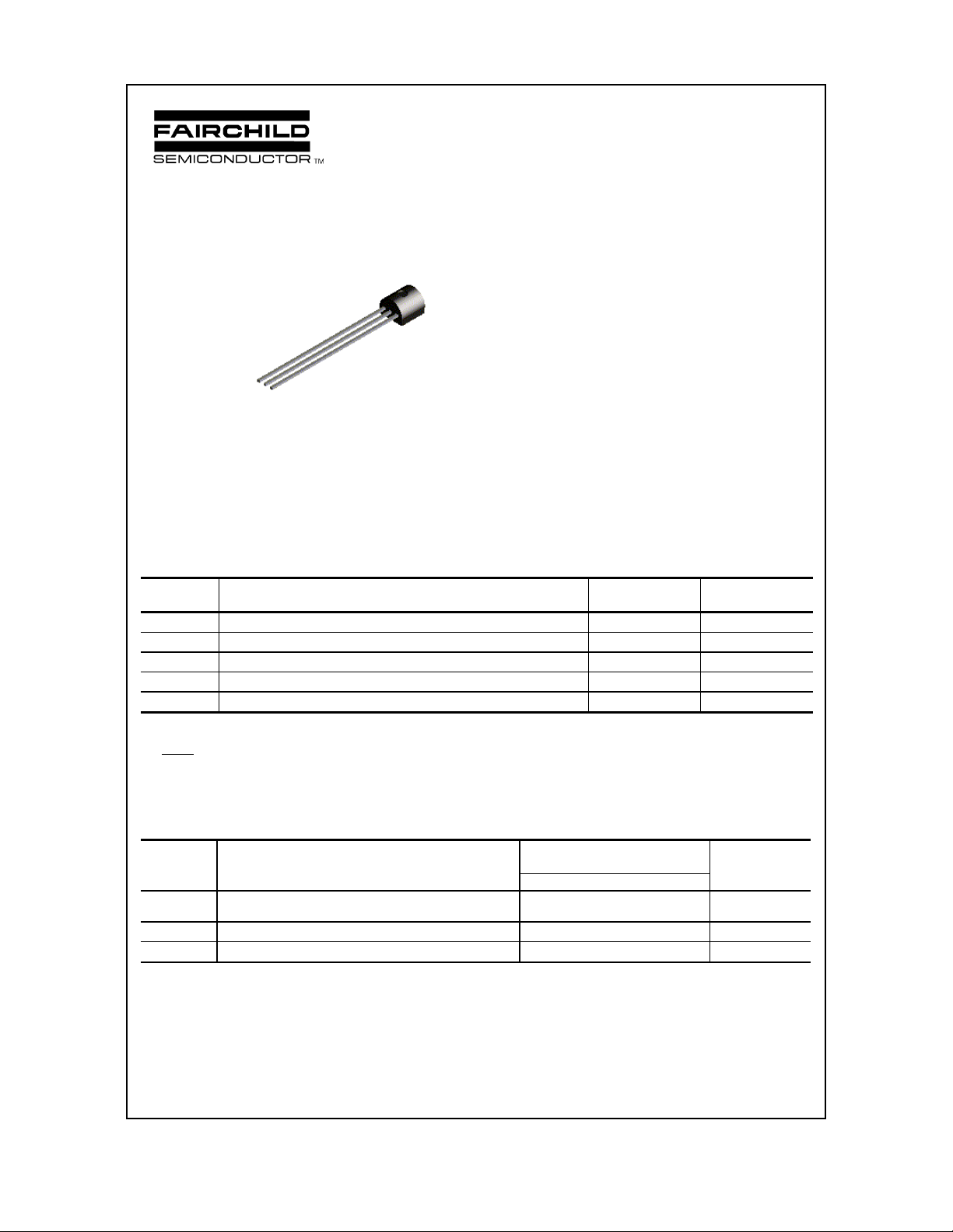
C
B
E
TO-92
NPN RF Transistor
This device is designed for use as RF amplifiers, oscillators and
multipliers with collector currents in the 1.0 mA to 30 mA range.
Sourced from Process 43. See PN918 for characteristics.
Absolute Maximum Ratings* TA = 25°C unless otherwise noted
Symbol Parameter Value Units
V
CEO
V
CBO
V
EBO
I
C
TJ, T
stg
*These ratings are limiting values above which the serviceability of any semiconductor device may be impaired.
NOTES:
1) These ratings are based on a maximum junction temperature of 150 degrees C.
2) These are steady state limits. The factory should be consulted on applications involving pulsed or low duty cycle operations.
Thermal Characteristics TA = 25°C unless otherwise noted
Collector-Emitter Voltage 15 V
Collector-Base Voltage 30 V
Em i t ter - Bas e V olt ag e 4. 5 V
Collector Current - Continuous 50 mA
Operating and Storage Junction Temperature Range -55 to +150
°C
Symbol Characteri st ic Max Un i ts
2N5770
P
D
R
θ
JC
R
θ
JA
1997 Fairchild Semiconductor Corporation
Total De vice Dissipat i on
Derate above 25°C
Thermal Resistance, Junction to Case 125
Thermal Resistance, Junction to Ambient 357 °C/W
350
2.8
mW
mW/°C
°C/W
NPN RF Transistor
(continued)
Electrical Characteristics TA = 25°C unless otherwise noted
Symbol Parameter Test Conditions Min Max Units
OFF CHARACTERISTICS
V
(BR)CEO
V
(BR)CBO
V
(BR)EBO
I
CBO
I
EBO
ON CHARACTERISTICS*
h
FE
V
sat
CE(
V
sat
BE(
Collector-Emitter Breakdown Voltage* IC = 3.0 mA, IB = 0 15 V
Collector-Base Breakdown Voltage
= 1.0 µA, IE = 0
I
C
30 V
Em itter-B ase Breakdown Voltag e IE = 10 µA, IC = 0 4.5 V
Collector Cutoff Current VCB = 15 V, IE = 0
V
= 15 V, IE = 0, TA = 150 °C
CB
Em it ter C u to ff C ur rent VEB = 3.0 V, IC = 0
V
= 2.0 V, IC = 0
EB
DC Cu r ren t Gain VCE = 1.0 V, IC = 3.0 mA
= 10 V, IC = 8.0 mA
V
Collector-Emitter Saturation Voltage IC = 10 mA, IB = 1.0 mA 0.4 V
)
Base- Emi tt er Saturation Voltage IC = 10 mA, IB = 1.0 mA 1.0 V
)
CE
20
50 200
10
1.0
10
1.0
nA
µ
µ
µ
A
A
A
2N5770
SMALL SIGNAL CHARACTERISTICS
NF Noise Figure IC = 1.0 mA, VCE = 8.0 V,
f = 60 MHz, Rg = 400 Ω
C
cb
C
ib
h
fe
Collector-Base Capacitance VCB = 10 V, IE = 0, f = 1.0 MHz 0.7 1.1 pF
Input Capacitance VEB = 0.5 V 2.0 pF
Small-Signal Current Gain IC = 8.0 mA, VCE = 10 V,
f = 100 MHz
= 8.0 mA, VCE = 10 V,
I
C
f = 1. 0 kHz
rb’C
C
Collector-Base Time Constant IE = 8.0 mA, VCB = 10 V,
f = 79.8 MHz
9.0
40
3.0 20 pS
6.0 dB
18
240
FUNCTIONAL TEST
G
pe
P
O
Ampl ifier Po wer Gain IC = 6.0 mA, VCB = 12 V,
f = 20 0 M Hz
Power Output VCC = 15 V, IC = 8.0 mA, 30 mW
η Col lec t or Eff icien cy f = 50 0 M Hz 2 5 %
15 dB
*Pulse Test: Pulse Width ≤ 300 µs, Duty Cycle ≤ 2.0%
 Loading...