

Fairchild Semiconductor 2N5638 Datasheet
2N5638
N-Channel Switch
• This device is designed for low level analog switchng, sample and hold
circuits and chopper stabilized amplifiers.
• Sourced from process 51.
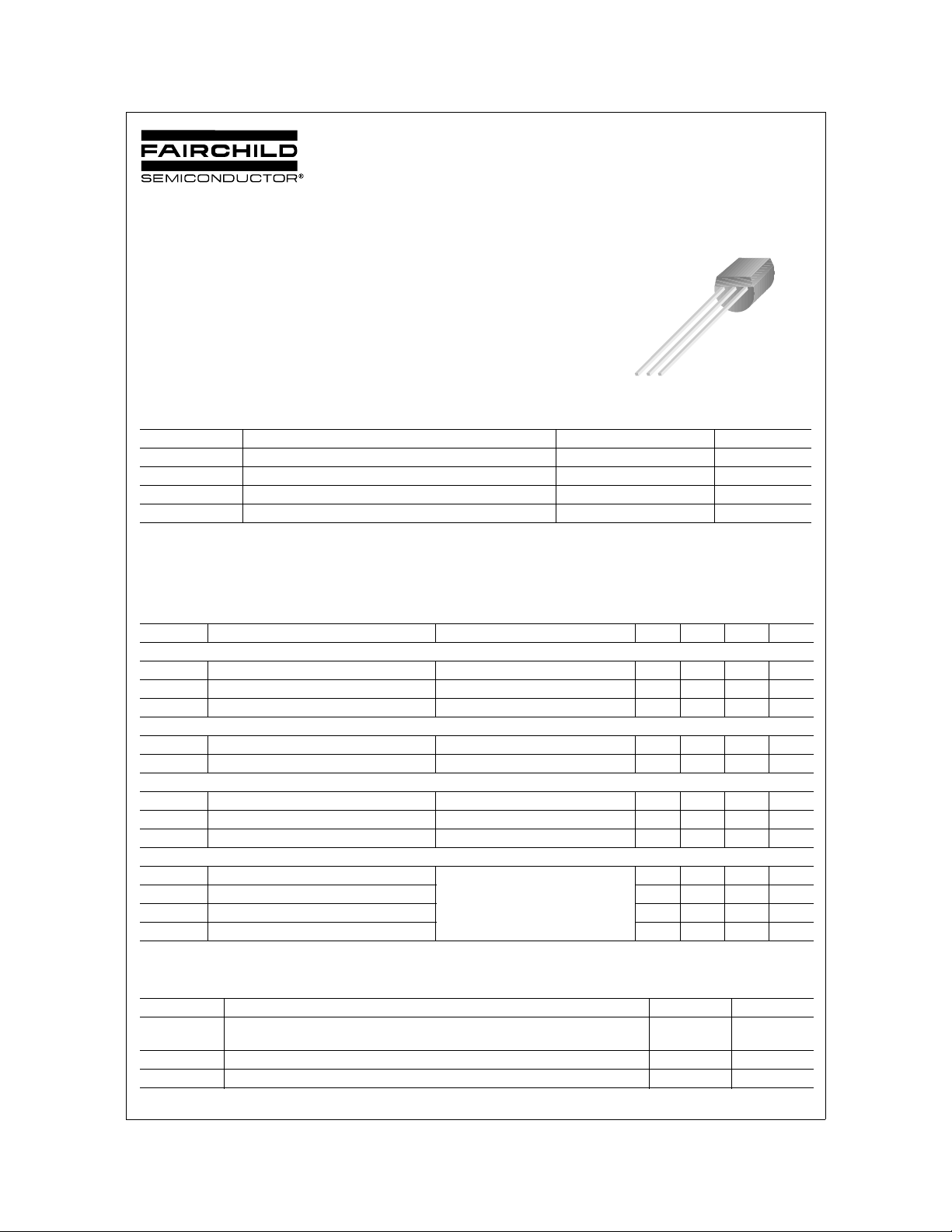
2N5638
1
TO-92
1. Drain 2. Source 3. Gate
Absolute Maximum Ratings *
TC=25°C unless otherwise noted
Symbol Parameter Value Units
V
DG
V
GS
I
GF
T
, T
J
STG
* These ratings are limiting values above which the serviceability of any semiconductor device may be impaired.
NOTES:
1. These ratings are based on a maximum junction temperature of 150 degrees C.
2. These are steady state limits. The factory should be consulted on applications involving pulsed or low duty cycle operations.
Electrical Characteristics
Drain-Gate Voltage 30 V
Gate-Source Voltage -30 V
Forward Gate Current 50 mA
Operating and Storage Junction Temperature Range -55 ~ +150 °C
TC=25°C unless otherwise noted
Symbol Parameter Test Condition Min. Typ. Max. Units
Off Characteristics
V
(BR)GSS
I
GSS
I
D(off)
Gate-Source Breakdown Voltage VDS = 0, IG = -10µA-30 V
Gate Reverse Current VGS = -15V, VDS = 0 -1.0 nA
Drain Cutoff Leakage Current VDS = 12V, VGS = 15V 1.0 nA
On Characteristics
I
DSS
r
DS(on)
Zero-Gate Voltage Drain Current * VDS = 20V, IGS = 0 50 mA
Drain-Source On Resistance VGS = 0V, ID = 1.0mA 30 Ω
Small Signal Characteristics
r
ds(on)
C
iss
C
rss
Drain-Source On Resistance VDS = VGS = 0, f = 1.0kHz 30 Ω
Input Capacitance VDS = 0, VGS = 12V, f = 1.0MHz 10 pF
Reverse Transfer Capacitance VDS = 0V, VGS = 12V, f = 1.0MHz 4.0 pF
Switching Characteristics
t
d(on)
t
r
t
d(off)
t
f
* Pulse Test: Pulse Width ≤ 300µs, Duty Cycle ≤ 1.0%
Trun On Delay Time VDD = 10V, V
= -12, I
V
Rise Time 5.0 ns
Trun Off Delay Time 5.0 ns
GS(off)
R
G
= 50Ω
GS(on)
D(on)
= 0
= 12mA
4.0 ns
Fall Time 10 ns
Thermal Characteristics
TA=25°C unless otherwise noted
Symbol Parameter Max. Units
P
D
R
θJC
R
θJA
©2002 Fairchild Semiconductor Corporation Rev. A1, November 2002
Total Device Dissipation
Derate above 25°C
350
2.8
mW
mW/°C
Thermal Resistance, Junction to Case 125 °C/W
Thermal Resistance, Junction to Ambient 357 °C/W
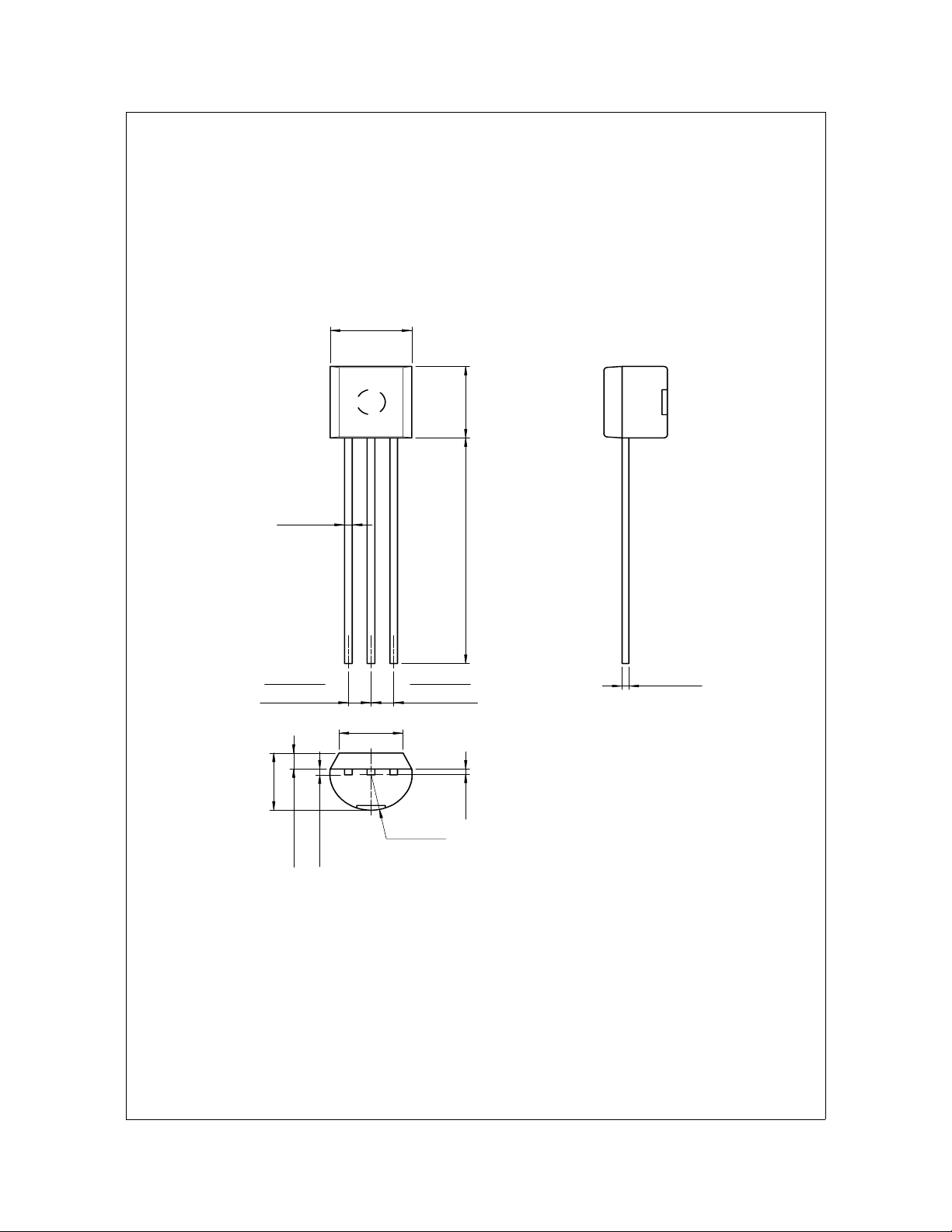
Package Dimensions
0.46
±0.10
4.58
+0.25
–0.15
2N5638
TO-92
±0.20
4.58
±0.40
1.27TYP
[1.27
±0.20
3.86MAX
±0.10
1.02
+0.10
–0.05
0.38
14.47
1.27TYP
]
3.60
±0.20
[1.27
±0.20
]
0.38
+0.10
–0.05
(0.25)
(R2.29)
Dimensions in Millimeters
©2002 Fairchild Semiconductor Corporation Rev. A1, November 2002
 Loading...