Fairchild FXLH1T45 Service Manual

tm
FXLH1T45 Low Voltage 1-Bit Bi-directional Level Translator with Configurable Voltage Supplies and Bushold Data Inputs
April 2007
FXLH1T45
Low Voltage 1-Bit Bi-directional Level Translator with
Configurable Voltage Supplies and Bushold Data Inputs
Features
Bi-directional interface between any 2 levels from 1.1V
■
to 3.6V
■
Fully configurable: Inputs track V
Non-preferential power-up sequencing; either V
■
may be powered-up first
Outputs remain in 3-STATE until active V
■
reached
■
Outputs switch to 3-STATE if either V
Power off protection
■
■
Bushold on data inputs eliminates the need for
external pull-up/pull-down resistors
Control input (T/R
■
) levels are referenced to V
voltage
■
Packaged in the MicroPak 6 (1.0mm x 1.45mm)
ESD protections exceeds:
■
– 4kV HBM ESD
(per JESD22-A114 & Mil Std 883e 3015.7)
– 8kV HBM I/O to GND ESD
(per JESD22-A114 & Mil Std 883e 3015.7)
– 1kV CDM ESD (per ESD STM 5.3)
– 200V MM ESD (per JESD22-A115 & ESD STM5.2)
CC
level
CC
level is
CC
is at GND
CCA
CC
General Description
The FXLH1T45 is a single bit configurable dual-voltage
supply translator designed for both uni-directional and
bi-directional voltage translation between two logic levels. The device allows translation between voltages as
high as 3.6V to as low as 1.1V. The A port tracks the
V
level, and the B port tracks the V
CCA
level. This
CCB
allows for bi-directional voltage translation over a variety
of voltage levels: 1.2V, 1.5V, 1.8V, 2.5V, and 3.3V.
The device remains in 3-STATE until both V
active levels allowing either V
to be powered-up first.
CC
s reach
CC
Internal power down control circuits place the device in
3-STATE if either V
The Transmit/Receive (T/R
is removed.
CC
) input determines the direction of data flow through the device. The FXLH1T45 is
designed so that the control pin (T/R
V
.
CCA
) is supplied by
Ordering Information
Package
Order Number
FXLH1T45L6X MAC06A Yes 6-Lead MicroPak, 1.0mm Wide 5k Units on Tape and Reel
MicroPak™ is a trademark of Fairchild Semiconductor Corporation.
©2006 Fairchild Semiconductor Corporation www.fairchildsemi.com
FXLH1T45 Rev. 1.0.4
Number Pb-Free Package Description Supplied As

H =
FXLH1T45 Low Voltage 1-Bit Bi-directional Level Translator with Configurable Voltage Supplies and Bushold Data Inputs
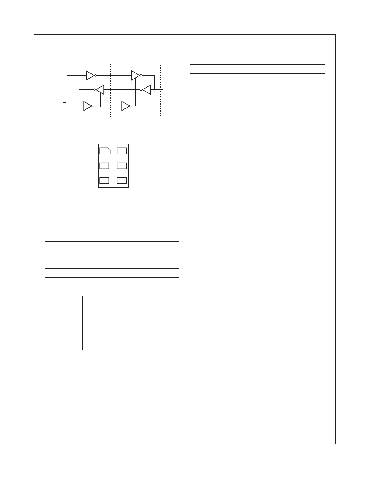
Functional Diagram
V
CCA
A
T/R
Connection Diagram
1
V
CCA
2
GND
34
A
6
5
(Top Through View)
Pin Assignment
Pin Number Terminal Name
1V
2 GND
3A
4B
5 T/R
6V
V
CCB
V
CCB
T/R
B
CCA
CCB
Function Table
Inputs (T/R
B
HIGH Logic Level
L = LOW Logic Level
) Outputs
L Bus B Data to Bus A
H Bus A Data to Bus B
Power-Up/Power-Down Sequencing
FXL translators offer an advantage in that either V
may be powered up first. This benefit derives from the
chip design. When either V
is at 0V, outputs are in a
CC
HIGH-Impedance state. To ensure that bus contention,
excessive currents, or oscillations do not occur, a proper
power-up sequence is recommended.
The recommended power-up sequence is the following:
1. Apply power to either V
2. Apply power to the T/R
.
CC
input (Logic HIGH for A-to-B
operation; Logic LOW for B-to-A operation) and to the
respective data inputs (A Port or B Port). This may
occur at the same time as Step 1.
3. Apply power to other V
CC
.
The recommended power-down sequence is the following:
1. Remove power from either V
2. Remove power from other V
CC
CC
.
.
CC
Pin Descriptions
Pin Names Description
T/R
A Side A Input or Output
B Side B Input or Output
V
CCA
V
CCB
©2006 Fairchild Semiconductor Corporation www.fairchildsemi.com
FXLH1T45 Rev. 1.0.4 2
Tr ansmit/Receive Input
Side A Power Supply
Side B Power Supply

±
±
±
±
−
−
−
−
) −
−
+
−
+
<
−
<
>
−
+
−
±
− 65 °
±
− 40 °
∆
∆
=
FXLH1T45 Low Voltage 1-Bit Bi-directional Level Translator with Configurable Voltage Supplies and Bushold Data Inputs
Absolute Maximum Ratings
Stresses exceeding the absolute maximum ratings may damage the device. The device may not function or be
operable above the recommended operating conditions and stressing the parts to these levels is not recommended.
In addition, extended exposure to stresses above the recommended operating conditions may affect device reliability.
The absolute maximum ratings are stress ratings only.
Symbol Parameter Rating
V
CCA
I
OH
T
, V
V
V
I
IK
I
OK
I
CC
STG
CCB
I
O
/
I
OL
Supply Voltage
DC Input Voltage
I/O Port A
I/O Port B
Control Input (T/R
Output Voltage
)
(1)
Outputs 3-STATE
Outputs Active (A
Outputs Active (B
DC Input Diode Current @ V
)
n
n
I
DC Output Diode Current @
V
0V
O
V
V
O
CC
DC Output Source/Sink Current
DC V
or Ground Current per Supply Pin
CC
Storage Temperature Range
0V
0.5V to + 4.6V
0.5V to + 4.6V
0.5V to + 4.6V
0.5V to + 4.6V
0.5V to + 4.6V
0.5V to V
0.5V to V
50mA / + 50mA
0.5V
CCA
0.5V
CCB
50mA
50mA
50mA
100mA
C to + 150 ° C
Recommended Operating Conditions
(2)
The Recommended Operating Conditions table defines the conditions for actual device operation. Recommended
operating conditions are specified to ensure optimal performance to the datasheet specifications. Fairchild does not
recommend exceeding them or designing to absolute maximum ratings.
Symbol Parameter Rating
V
or V
CCA
CCB
T
A
t
V Maximum Input Edge Rate V
/
Notes:
1. I
Absolute Maximum Rating must be observed.
O
2. All unused inputs
Power Supply Operating 1.1V to 3.6V
Input Voltage
Por t A
Por t B
Control Input (T/R
Output Current in I
OH
)
/I
with V
OL
3.0V to 3.6V
2.3V to 2.7V
1.65V to 1.95V
1.4V to 1.65V
1.1V to 1.4V
Free Air Operating Temperature
and I/O pins
must be held at V
CCI
CC @
1.1V to 3.6V 10ns/V
CCA/B
or GND.
0.0V to 3.6V
0.0V to 3.6V
0.0V to V
24mA
18mA
6mA
2mA
0.5mA
C to + 85 ° C
CCA
©2006 Fairchild Semiconductor Corporation www.fairchildsemi.com
FXLH1T45 Rev. 1.0.4 3

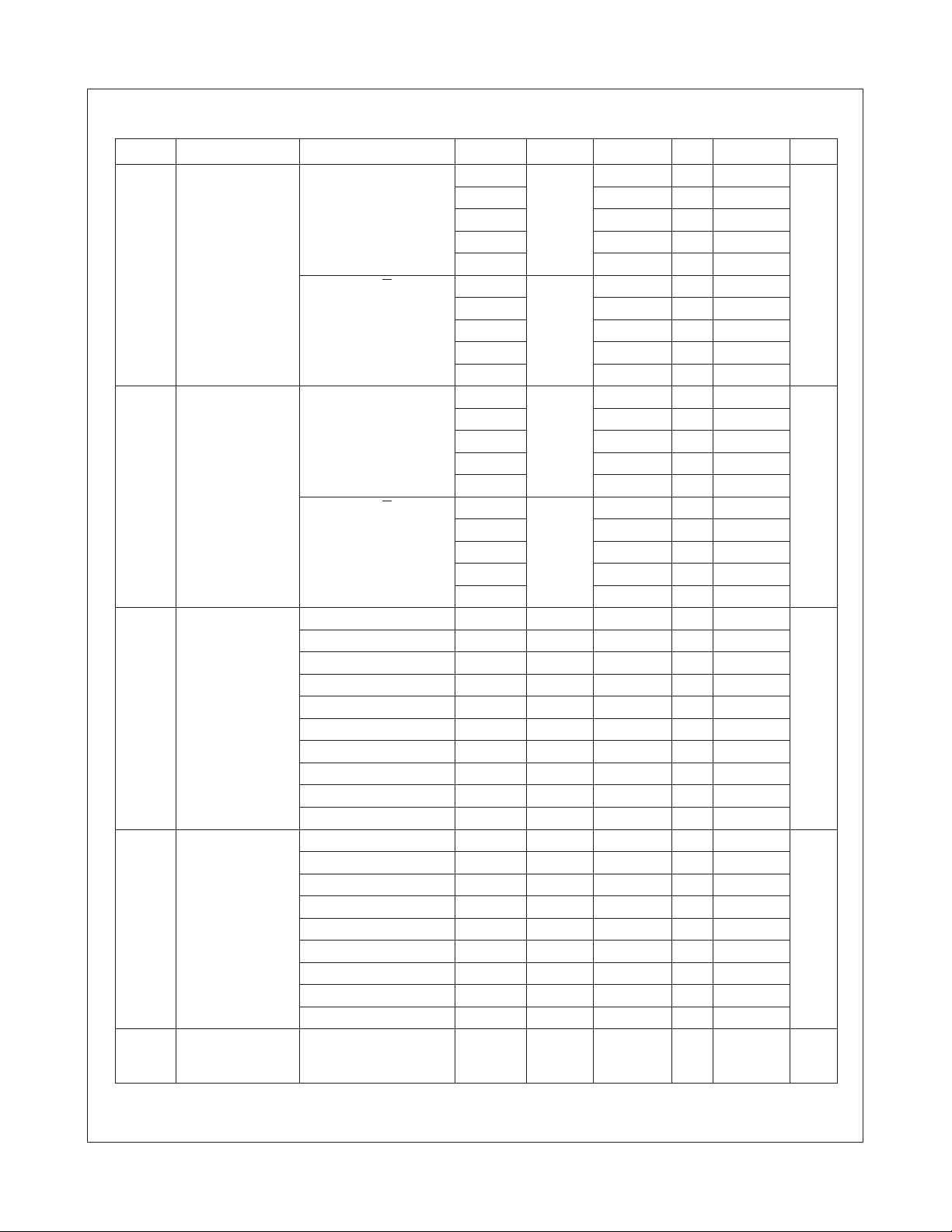
DC Electrical Characteristics
Symbol Parameter Conditions
V
High Level Input
IH
Low Level Input
V
IL
VOH High Level Output
Low Level Output
V
OL
I
I
(3)
Voltage
(3)
Voltage
(4)
Voltage
(4)
Voltage
Input Leakage
Current Control
Pins
Data Inputs A
, B
n
Control Pin T/R
(Referenced to V
Data Inputs An, B
Control Pin T/R
(Referenced to V
IOH = −100µA 1.1–3.6 1.1–3.6 V
= −12mA 2.7 2.7 2.2 – –
I
OH
= −18mA 3.0 3.0 2.4 – –
I
OH
= −24mA 3.0 3.0 2.2 – –
I
OH
= −6mA 2.3 2.3 2.0 – –
I
OH
= −12mA 2.3 2.3 1.8 – –
I
OH
= −18mA 2.3 2.3 1.7 – –
I
OH
= −6mA 1.65 1.65 1.25 – –
I
OH
= −2mA 1.4 1.4 1.05 – –
I
OH
= −0.5mA 1.1 1.1 0.75 x V
I
OH
IOL = 100µA 1.1–3.6 1.1–3.6 – – 0.2 V
= 12mA 2.7 2.7 – – 0.4
I
OL
= 18mA 3.0 3.0 – – 0.4
I
OL
= 24mA 3.0 3.0 – – 0.55
I
OL
=12mA 2.3 2.3 – – 0.4
I
OL
= 18mA 2.3 2.3 – – 0.6
I
OL
= 6mA 1.65 1.65 – – 0.3
I
OL
= 2mA 1.4 1.4 – – 0.35
I
OL
= 0.5mA 1.1 1.1 – – 0.3 x V
I
OL
VI = V
or GND 1.1–3.6 3.6 – – ±1.0 µA
CCA
n
CCA
n
CCA
V
CCI
(V) V
CCO
(V)
Min. Typ. Max. Units
2.7–3.6 1.1–3.6 2.0 – – V
2.3–2.7 1.6 – –
1.65–2.3 0.65 x V
1.4–1.65 0.65 x V
1.1–1.4 0.9 x V
––
CCI
––
CCI
––
CCI
2.7–3.6 1.1–3.6 2.0 – –
)
2.3–2.7 1.6 – –
1.65–2.3 0.65 x V
1.4–1.65 0.65 x V
1.1–1.4 0.9 x V
CCA
––
CCA
––
CCA
––
2.7–3.6 1.1–3.6 – – 0.8 V
2.3–2.7 – – 0.7
1.65–2.3 – – 0.35 x V
1.4–1.65 – – 0.35 x V
1.1–1.4 – – 0.1 x V
2.7–3.6 1.1–3.6 – – 0.8
)
2.3–2.7 – – 0.7
1.65–2.3 – – 0.35 x V
1.4–1.65 – – 0.35 x V
1.1–1.4 – – 0.1 x V
–0.2 – – V
CC0
––
CC0
CCI
CCI
CCI
CCA
CCA
CCA
CC0
FXLH1T45 Low Voltage 1-Bit Bi-directional Level Translator with Configurable Voltage Supplies and Bushold Data Inputs
©2006 Fairchild Semiconductor Corporation www.fairchildsemi.com
FXLH1T45 Rev. 1.0.4 4
 Loading...