Fairchild FAN73933 service manual
FAN73933
Half-Bridge Gate Drive IC
FAN73933 — Half-Bridge Gate Driver
December 2009
Features
Floating Channel for Bootstrap Operation to +600V
Typically 2.5A/2.5A Sourcing/Sinking Current Driving
Capability
Extended Allowable Negative V
Signal Propagation at VBS=15V
Output in Phase with Input Signal
3.3V and 5V Input Logic Compatible
Matched Propagation Delay for Both Channels
Built-in UVLO Functions for Both Channels
Built-in Common-Mode dv/dt Noise Cancelling Circuit
Programmable Dead-Time Control Function
Internal 220ns Minimum Dead Time at R
Swing to -9.8V for
S
=0Ω
DT
Applications
High-Speed Power MOSFET and IGBT Gate Driver
Induction Heating
High-Power DC-DC Converter
Synchronous Step-Down Converter
Motor Drive Inverter
Description
The FAN73933 is a half-bridge, gate-drive IC with programmable dead-time control functions that can drive
high-speed MOSFETs and IGBTs operating up to +600V.
It has a buffered output stage with all NMOS transistors
designed for high-pulse-current driving capability and
minimum cross-conduction.
Fairchild’s high-voltage process and common-mode
noise canceling techniques provide stable operation of
the high-side driver under high dv/dt noise circumstances. An advanced level-shift circuit offers high-side
gate driver operation up to V
V
=15V.
BS
The UVLO circuit prevents malfunction when V
are lower than the specified threshold voltage.
V
BS
The high-current and low-output voltage drop feature
makes this device suitable for diverse half- and fullbridge inverters; motor drive inverters, switching mode
power supplies, induction heating, and high-power DCDC converter applications.
14-SOP
=-9.8V (typical) for
S
DD
and
Ordering Information
Operating
Part Number Package
Temperature
Range
FAN73933M 14-Lead, Small Outline Integrated
FAN73933MX Tape & Reel
For Fairchild’s definition of Eco Status, please visit: http://www.fairchildsemi.com/company/green/rohs_green.html.
© 2009 Fairchild Semiconductor Corporation www.fairchildsemi.com
FAN73933 • Rev. 1.0.0
Circuit (SOIC), Non-JEDEC, .150
Inch Narrow Body, 225SOP
-40°C to +125°C RoHS
Eco
Status
Packing Method
Tube
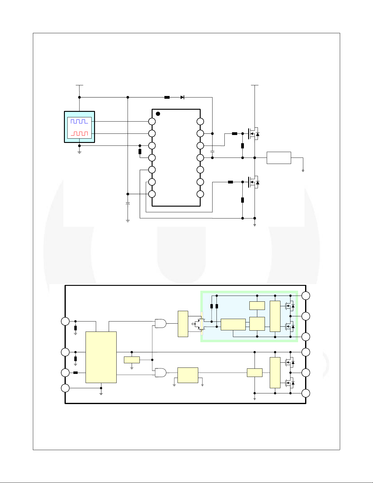
Typical Application Diagrams
FAN73933 — Half-Bridge Gate Driver
+15V
Controller
HIN
LIN
D
R
BOOT
BOOT
FAN73933
HIN
1
LIN
2
V
3
R
DT
SS
DT
4
5
COM
LO
6
V
7
DD
NC1214
13
V
B
HO
V
11
S
10
NC
NC
NC
9
8
Figure 1. Typical Application Circuit
C
Up to 600V
R1
R2
BOOT
Load
R3
R4
Internal Block Diagram
1
HIN
250K
SCHMITT
TRIGGER INPUT
2
LIN
V
DT
4
3
SS
SHOOT THOUGH
250K
PREVENTION
R
DTINT
DEAD-TIME
{ DTMIN=220ns }
Pin 8, 9, 10 and 14 are no connection
GENERATOR
HS(ON/OFF)
UVLO
LS(ON/OFF)
PULSE
VSS/COM
LEVEL
SHIFT
Figure 2. Functional Block Diagram
NOISE
CANCELLER
UVLO
R
S
DELAY
13
V
B
DRIVER
12
R
Q
HO
11
V
S
7
V
DD
DRIVER
6
LO
5
COM
© 2009 Fairchild Semiconductor Corporation www.fairchildsemi.com
FAN73933 • Rev. 1.0.0 2
Pin Configuration
HIN
FAN73933 — Half-Bridge Gate Driver
1
14
NC
LIN
V
SS
DT
COM
LO
V
DD
2
3
4
5
6
7
FAN73933
13
12
11
10
9
8
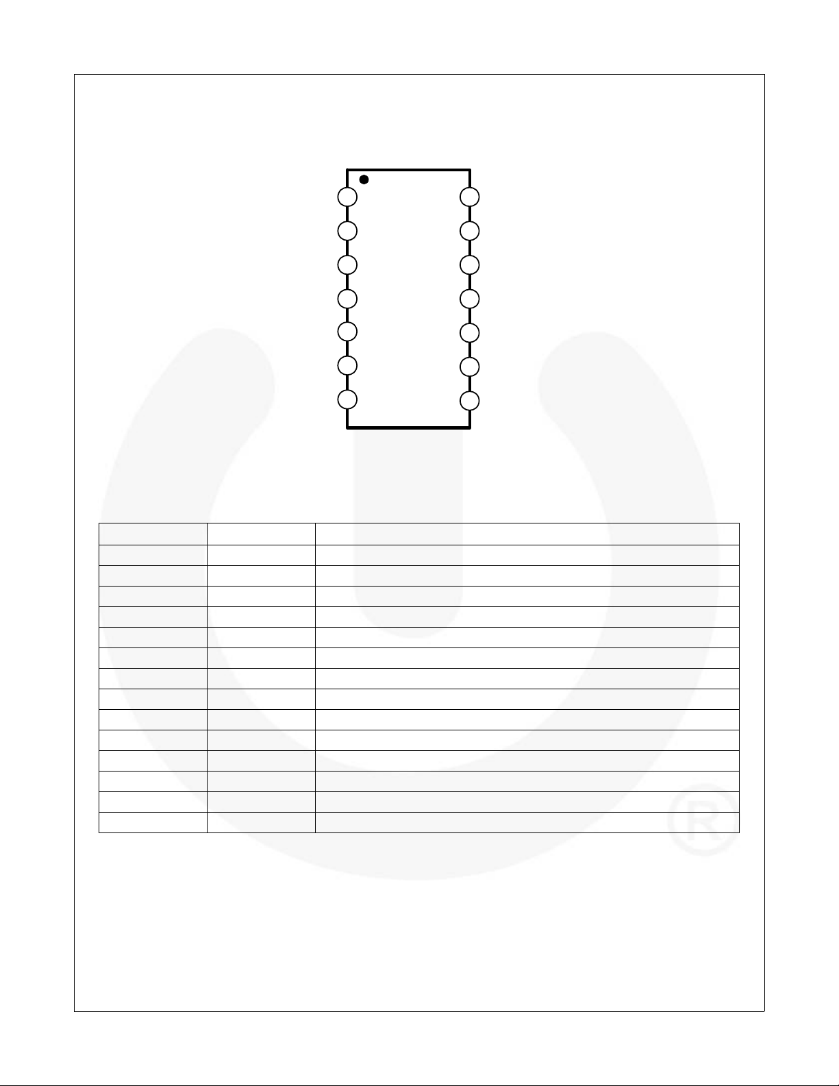
Figure 3. Pin Configurations (Top View)
Pin Definitions
Pin # Name Description
1 HIN Logic Input for High-Side Gate Driver Output
2 LIN Logic Input for Low-Side Gate Driver Output
3V
SS
4 DT Dead-Time Control with External Resistor (Referenced to V
5 COM Ground
6 LO Low-Side Driver Return
7V
DD
8 NC No Connection
9 NC No Connection
10 NC No Connection
11 V
S
12 HO High-Side Driver Output
13 V
B
14 NC No Connection
Logic Ground
Supply Voltage
High-Voltage Floating Supply Return
High-Side Floating Supply
V
HO
V
NC
NC
NC
B
S
)
SS
© 2009 Fairchild Semiconductor Corporation www.fairchildsemi.com
FAN73933 • Rev. 1.0.0 3
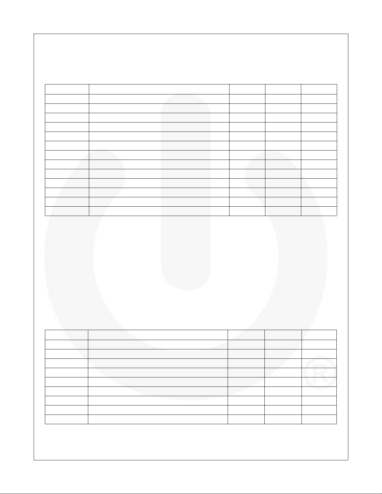
Absolute Maximum Ratings
Stresses exceeding the absolute maximum ratings may damage the device. The device may not function or be operable above the recommended operating conditions and stressing the parts to these levels is not recommended. In addition, extended exposure to stresses above the recommended operating cond itions may affect device reliability. The
absolute maximum ratings are stress ratings only. T
Symbol Characteristics Min. Max. Unit
V
B
V
S
V
HO
V
LO
V
DD
V
IN
DT Programmable Dead-Time Pin Voltage -0.3 V
V
SS
/dt Allowable Offset Voltage Slew Rate ± 50 V/ns
dV
S
P
D
θ
JA
T
J
T
STG
Notes:
1 Mounted on 76.2 x 114.3 x 1.6mm PCB (FR-4 glass epoxy material).
2 Refer to the following standards:
JESD51-2: Integral circuits thermal test method environmental conditions - natural convection, and
JESD51-3: Low effective thermal conductivity test board for leaded surface mount packages.
3 Do not exceed maximum P
High-Side Floating Supply Voltage -0.3 625.0 V
High-Side Floating Offset Voltage VB-25.0 VB+0.3 V
High-Side Floating Output Voltage VS-0.3 VB+0.3 V
Low-Side Output Voltage -0.3 VDD+0.3 V
Low-Side and Logic Fixed Supply Voltage -0.3 25.0 V
Logic Input Voltage (HIN and LIN) -0.3 VDD+0.3 V
Logic Ground VDD-25 VDD+0.3 V
Power Dissipation
(1, 2, 3)
Thermal Resistance 110 °C/W
Junction Temperature +150 °C
Storage Temperature -55 +150 °C
under any circumstances.
D
=25°C unless otherwise specified.
A
+0.3 V
DD
1W
FAN73933 — Half-Bridge Gate Driver
Recommended Operating Conditions
The Recommended Operating Conditions table defines the conditions for actual device operation. Recommended
operating conditions are specified to ensure optimal perfor mance to the datasheet specifications. Fairchild does not
recommend exceeding them or designing to absolute maximum ratings.
Symbol Parameter Min. Max. Unit
V
B
V
S
V
HO
V
DD
V
LO
V
IN
DT Programmable Dead-Time Pin Voltage V
V
SS
T
A
High-Side Floating Supply Voltage VS+10 VS+20 V
High-Side Floating Supply Offset Voltage 6-V
High-Side Output Voltage V
DD
S
600 V
V
B
V
Low-Side and Logic Fixed Supply Voltage 10 20 V
Low-Side Output Voltage COM V
Logic Input Voltage (HIN and LIN) V
SS
SS
DD
V
DD
V
DD
V
V
V
Logic Ground -5 +5 V
Operating Ambient Temperature -40 +125 °C
© 2009 Fairchild Semiconductor Corporation www.fairchildsemi.com
FAN73933 • Rev. 1.0.0 4
Electrical Characteristics
V
BIAS(VDD
parameters are referenced to VSS/COM and are applicable to the respective input leads: HIN a nd LIN. The VO and I
parameters are referenced to COM and are applicable to the respective output leads: HO and LO.
Symbol Characteristics Test Condition Min. Typ. Max. Unit
POWER SUPPLY SECTION
BOOTSTRAPPED SUPPLY SECTION
V
V
V
V
V
V
INPUT LOGIC SECTION
GATE DRIVER OUTPUT SECTION
Note:
4. These parameters guaranteed by design.
, VBS)=15.0V, VSS=COM=0V, DT=VSS and TA = 25°C, unless otherwise specified. The VIN and I
=0V or 5V
I
QDD
I
QBS
I
PDD
I
PBS
I
LK
DDUV+
BSUV+
DDUVBSUV-
DDUVH-
BSUVH
V
IH
V
IL
I
IN+
I
IN-
R
IN
V
OH
V
OL
I
O+
I
O-
V
S
Quiescent VDD Supply Current
Quiescent VBS Supply Current
Operating VDD Supply Current
Operating VBS Supply Current
Offset Supply Leakage Current
VDD and VBS Supply Under-Voltage
Positive-Going Threshold Voltage
VDD and VBS Supply Under-Voltage
Negative-Going Threshold Voltage
VDD and VBS Supply Under-Voltage Lockout
Hysteresis Voltage
Logic “1” Input Voltage for HO & Logic “0” for LO 2.5 V
Logic “0” Input Voltage for HO & Logic “1” for LO 0.8 V
Logic Input High Bias Current
Logic Input Low Bias Current
Logic Input Pull-Down Resistance 100 250 KΩ
High-Level Output Voltage (V
- VO) No Load 1.5 V
BIAS
Low-Level Output Voltage No Load 100 mV
Output High, Short-Circuit Pulsed Current
Output Low, Short-Circuit Pulsed Current
(4)
(4)
Allowable Negative VS Pin Voltage for IN Signal
Propagation to HO
V
IN
=0V or 5V
V
IN
=20KHz, No Load
f
IN
=1nF, fIN=20KHz, rms
C
L
=600V
V
B=VS
VIN=0V, VDD=VBS=Sweep
VIN=0V, VDD=VBS=Sweep
VIN=0V, VDD=VBS=Sweep
=5V
V
IN
=0V
V
IN
VHO=0V, VIN=5V, PW
≤10µs
VHO=15V,VIN=0V, PW
≤10µs
8.0 9.0 10 V
7.4 8.4 9.4 V
2.0 2.5 A
2.0 2.5 A
0.9 1.5 mA
50 100 μA
1.3 1.9 mA
450 800 μA
10 μA
0.6 V
20 50 μA
2 μA
-9.8 -7.0 V
FAN73933 — Half-Bridge Gate Driver
IN
O
© 2009 Fairchild Semiconductor Corporation www.fairchildsemi.com
FAN73933 • Rev. 1.0.0 5
Dynamic Electrical Characteristics
V
BIAS(VDD
Symbol Parameter Conditions Min. Typ. Max. Unit
Note:
5 The turn-on propagation display does not includ e dead time.
, VBS)=15.0V, VSS=COM=0V, CL=1000pF, DT=V
t
ON
t
OFF
Mt
ON
Mt
OFF
t
R
t
F
DT
MDT Dead-Time Matching=|DT
Turn-On Propagation Delay Time
Turn-Off Propagation Delay Time VS=0V 160 230 ns
Delay Matching, HO & LO Turn-On 0 50 ns
Delay Matching, HO & LO Turn-Off 0 50
Turn-On Rise Time VS=0V 40 60 ns
Turn-Off Fall Time VS=0V 20 35 ns
Dead Time: LO Turn-Off to HO Turn-On &
HO Turn-Off to LO Turn-On
LO-HO
(5)
- DT
HO-LO
and TA=25°C, unless otherwise specified.
SS
VS=0V, RDT=0Ω 160 230 ns
=0Ω 170 220 270 ns
R
DT
=300KΩ 400 500 600 ns
R
DT
=0Ω 050ns
R
DT
|
=300KΩ 0100ns
R
DT
FAN73933 — Half-Bridge Gate Driver
ns
© 2009 Fairchild Semiconductor Corporation www.fairchildsemi.com
FAN73933 • Rev. 1.0.0 6
 Loading...