Fairchild FAN7392 service manual
FAN7392
14-PDIP 16-SOP
High-Current, High- and Low-Side, Gate-Drive IC
FAN7392 — High-Current, High- and Low-Side, Gate-Drive IC
July 2012
Features
Floating Channel for Bootstrap Operation to +600V
3A/3A Sourcing/Sinking Current Driving Capability
Common-Mode dv/dt Noise Canceling Circuit
3.3V Logic Compatible
Separate Logic Supply (V
Under-Voltage Lockout for V
Cycle-by-Cycle Edge-Triggered Shutdown Logic
Matched Propagation Delay for Both Channels
Outputs In-phase with Input Signals
Available in 14-DIP and 16-SOP (Wide) Packages
) Range from 3.3V to 20V
DD
and V
CC
BS
Applications
High-Speed Power MOSFET and IGBT Gate Driver
Server Power Supply
Uninterrupted Power Supply (UPS)
Telecom System Power Supply
Distributed Power Supply
Motor Drive Inverter
Description
The FAN7392 is a monolithic high- and low-side gate
drive IC, that can drive high-speed MOSFETs and IGBTs
that operate up to +600V. It has a buffered output stage
with all NMOS transistors designed for high pulse current
driving capability and minimum cross-conduction. Fairchild’s high-voltage process and common-mode noise canceling techniques provide stable operation of the highside driver under high dv/dt noise circumstances. An
advanced level-shift circuit offers high-side gate driver
operation up to V
inputs are compatible with standard CMOS or LSTTL
output, down to 3.3V logic. The UVLO circuit prevents
malfunction when V
fied threshold voltage. The high-current and low-output
voltage drop feature makes this device suitable for halfand full-bridge inverters, like switching-mode power supply and high-power DC-DC converter applications.
=-9.8V (typical) for VBS=15V. Logic
S
and VBS are lower than the speci-
CC
Ordering Information
Part Number
FAN7392N
FAN7392M
FAN7392MX Tape and Reel
© 2009 Fairchild Semiconductor Corporation www.fairchildsemi.com
FAN7392 Rev. 1.0.4
Operating
Temperature Range
-40°C to +125°C
Package Packing Method
14-PDIP Tube
16-SOP
Tube
Typical Application Diagrams
D
BOOT
Q1
R
BOOT
C
BOOT
15V
Q2
C1
R2
R1
Up to 600V
Controller
HIN
LIN
LO
COM
V
B
V
S
V
DD
SD
HIN
NC
13
NC
HO
V
SS
NC
12
14
11
10
9
8
2
3
1
4
7
5
6
LIN
V
CC
SD
15V
Load
D
BOOT
Q1
R
BOOT
C
BOOT
15V
Q2
C1
R2
R1
Up to 600V
Controller
HIN
LIN
LO
COM
V
B
V
S
V
DD
SD
HIN
NC
15
NC
HO
V
SS
NC
14
16
13
12
11
10
2
3
1
4
8
6
7
LIN
V
CC
SD
15V
Load
NC
5
NC
9
FAN7392 — High-Current, High- and Low-Side, Gate-Drive IC
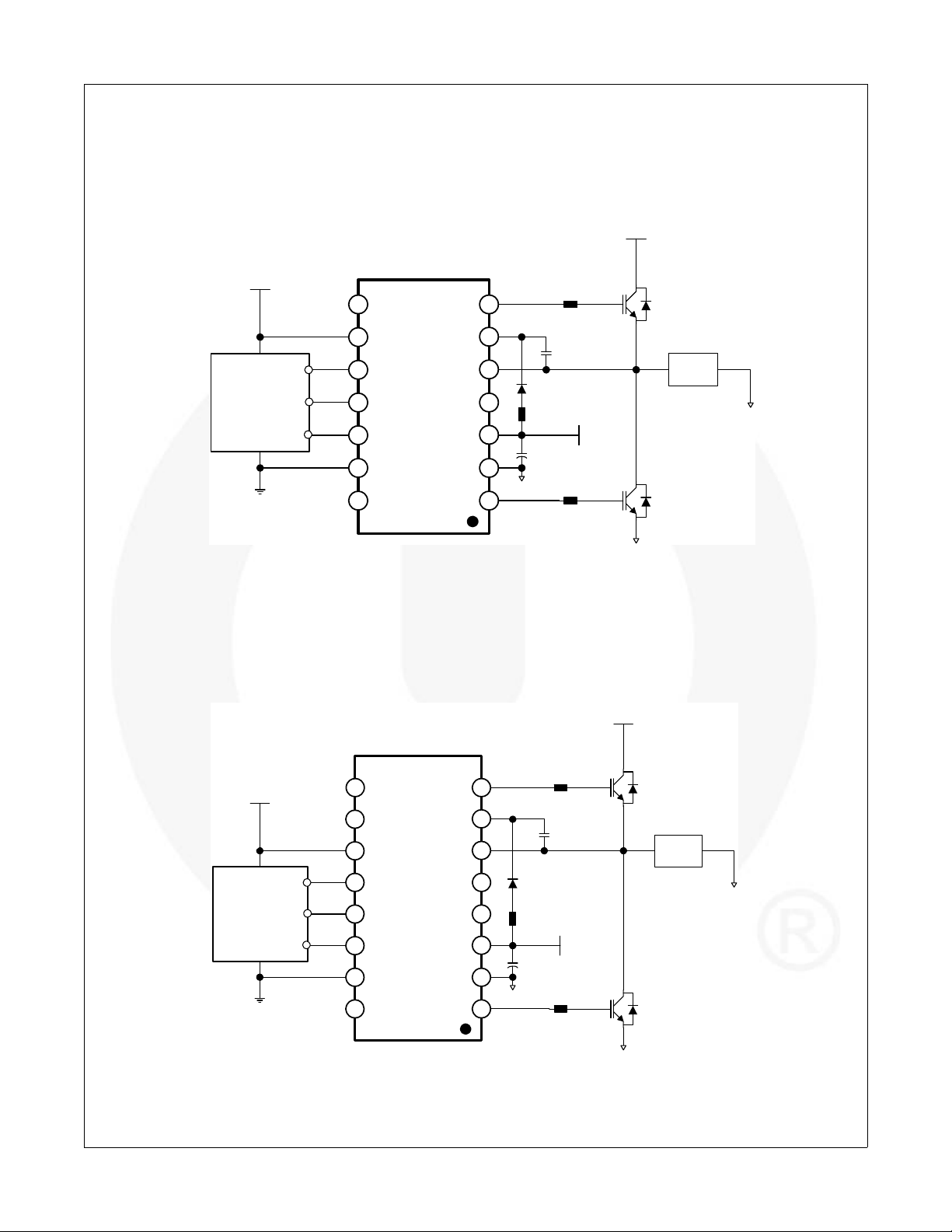
Figure 1. Typical Application Circuit (Referenced 14-DIP)
© 2009 Fairchild Semiconductor Corporation www.fairchildsemi.com
Figure 2. Typical Application Circuit (Referenced 16-SOP)
FAN7392 Rev. 1.0.4 2
Internal Block Diagram
UVLO
DRIVER
PULSE
GENERATOR
HIN
V
CC
COM
V
B
V
S
R
R
S
Q
DRIVER
HS(ON/OFF)
LS(ON/OFF)
DELAY
LIN
UVLO
HO
LO
SCHMITT
TRIGGER INPUT
CYCLE-By-CYCLE
EDGE TRIGGERED
SHUTDOWN
NOISE
CANCELLER
VSS/COM
LEVEL
SHIFT
V
SS
10
12
13
Pin 4, 8, and 14 are no connection
SD 11
V
DD
9
3
2
6
5
1
7
UVLO
DRIVER
PULSE
GENERATOR
HIN
V
CC
COM
V
B
V
S
R
R
S
Q
DRIVER
HS(ON/OFF)
LS(ON/OFF)
DELAY
LIN
UVLO
HO
LO
SCHMITT
TRIGGER INPUT
CYCLE-By-CYCLE
EDGE TRIGGERED
SHUTDOWN
NOISE
CANCELLER
VSS/COM
LEVEL
SHIFT
V
SS
12
14
15
Pin 4, 5, 9,10 and 16 are no connection
SD 13
VDD11
3
2
7
6
1
8
FAN7392 — High-Current, High- and Low-Side, Gate-Drive IC
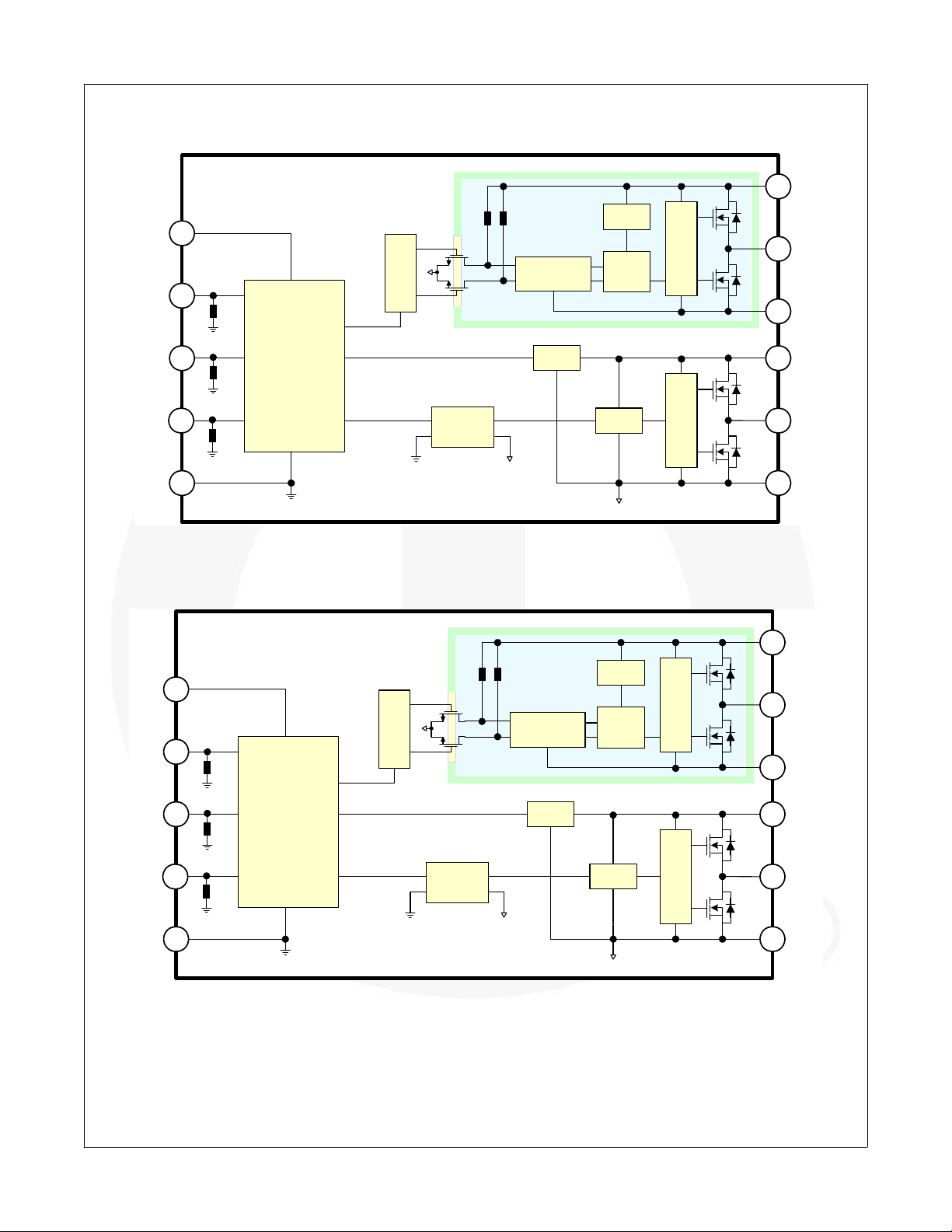
Figure 3. Functional Block Diagram (Referenced 14-Pin)
Figure 4. Functional Block Diagram (Referenced 16-SOP)
© 2009 Fairchild Semiconductor Corporation www.fairchildsemi.com
FAN7392 Rev. 1.0.4 3
Pin Configuration
LO
NC
FAN7392
HIN
HO NC
V
DD
COM
V
B
V
S
V
SS
1
2
3
4
5
6
7
14
13
12
11
10
9
8
SD
NC
V
CC
LIN
LO
NC
FAN7392M
HIN
HO
NC
V
DD
COM
V
B
V
S
V
SS
1
2
3
4
5
6
7
16
15
14
13
SD
NC
V
CC
LIN
12
11
10
98
NC
NC
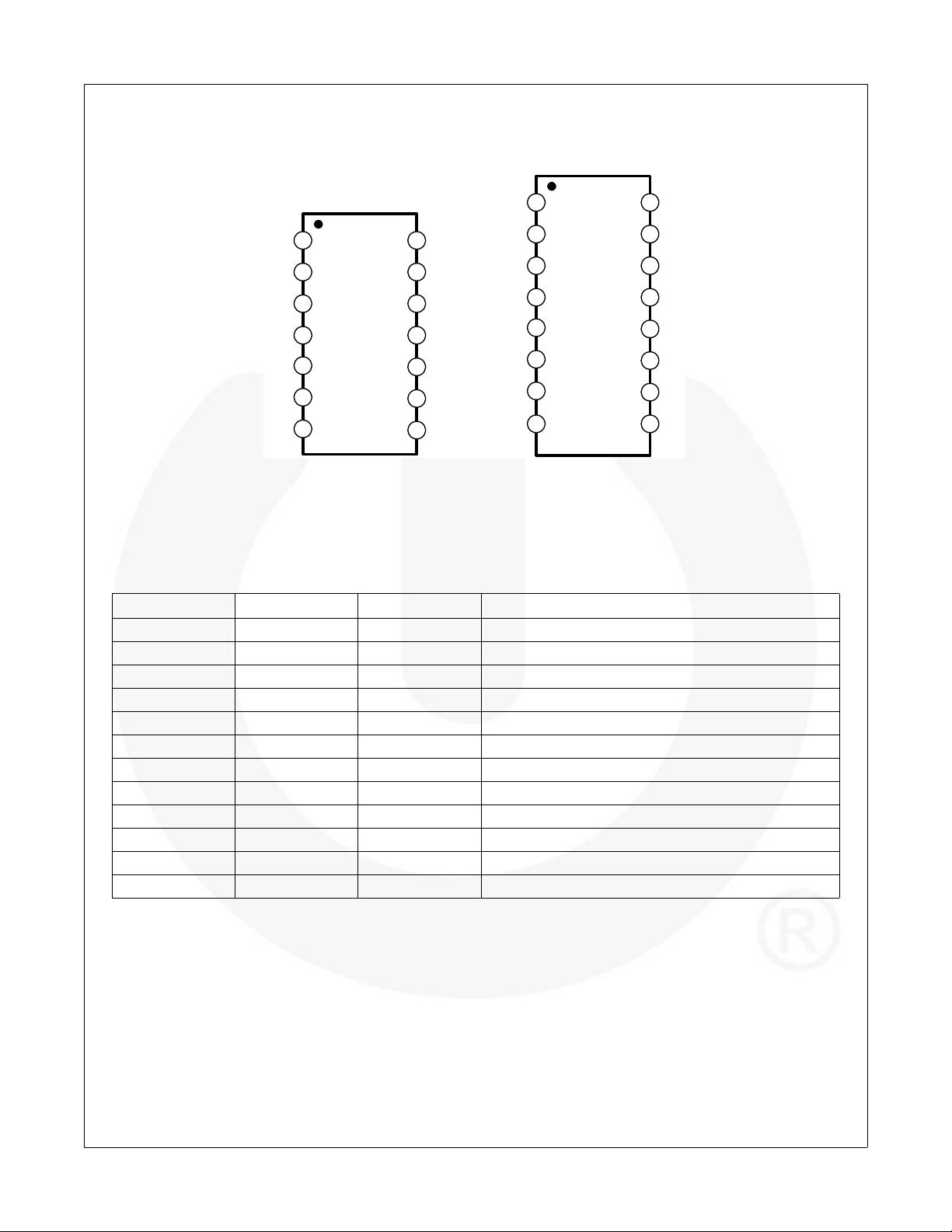
(a) 14-DIP (b) 16-SOP (Wide Body)
FAN7392 — High-Current, High- and Low-Side, Gate-Drive IC
Figure 5. Pin Configurations (Top View)
Pin Definitions
14-Pin 16-Pin Name Description
© 2009 Fairchild Semiconductor Corporation www.fairchildsemi.com
FAN7392 Rev. 1.0.4 4
1 1 LO Low-Side Driver Output
2 2 COM Low-Side Return
3 3 V
5 6 V
6 7 V
CC
S
B
Low-Side Supply Voltage
High-Voltage Floating Supply Return
High-Side Floating Supply
7 8 HO High-Side Driver Output
9 11 V
DD
Logic Supply Voltage
10 12 HIN Logic Input for High-Side Gate Driver Output
11 13 SD Logic Input for Shutdown Function
12 14 LIN Logic Input for Low-Side Gate Driver Output
13 15 V
SS
Logic Ground
4,8,14 4, 5, 9, 10, 16 NC No Connect
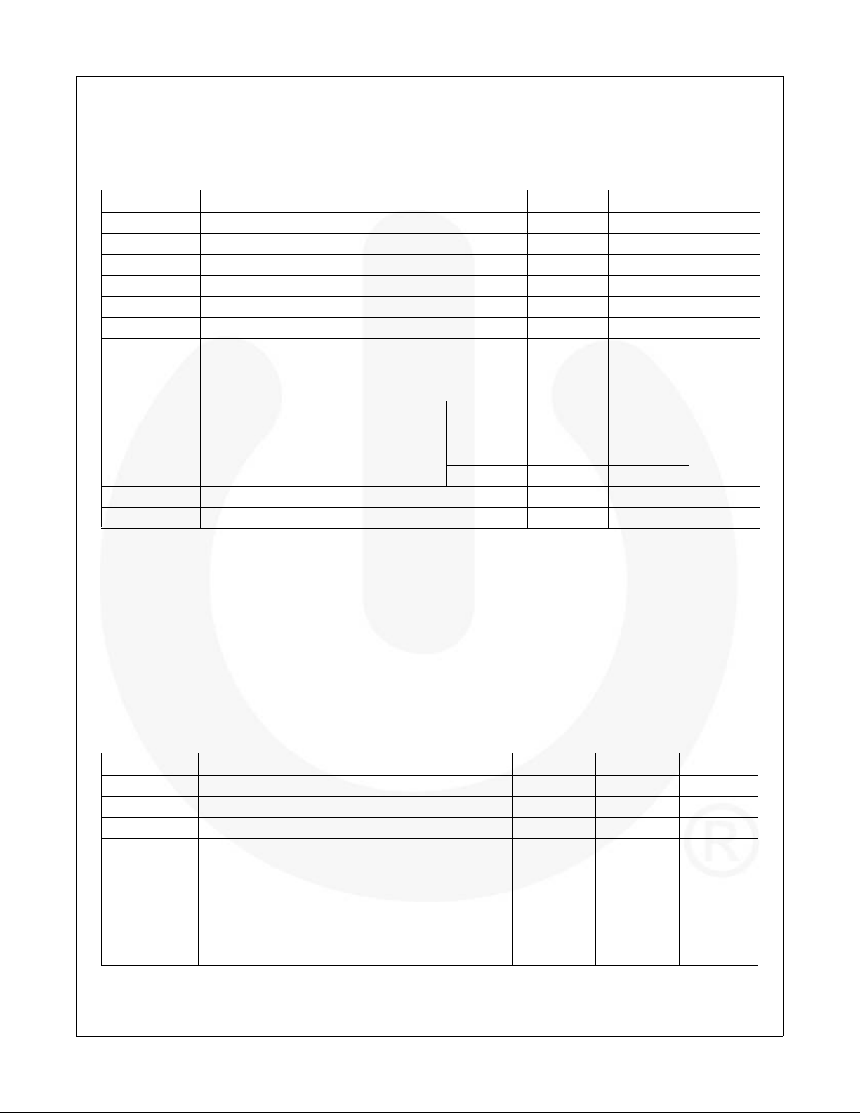
Absolute Maximum Ratings
Stresses exceeding the absolute maximum ratings may damage the device. The device may not function or be operable above the recommended operating conditions and stressing the parts to these levels is not recommended. In addition, extended exposure to stresses above the recommended operating cond itions may affect device reliability. The
absolute maximum ratings are stress ratings only. TA=25°C unless otherwise specified.
Symbol Characteristics Min. Max. Unit
V
B
V
S
V
HO
V
CC
V
LO
V
DD
V
SS
V
IN
dVS/dt Allowable Offset Voltage Slew Rate ±50 V/ns
P
D
JA
T
J
T
STG
Notes:
1. Mounted on 76.2 x 114.3 x 1.6mm PCB (FR-4 glass epoxy material).
2. Refer to the following standards:
JESD51-2: Integral circuits thermal test method environmental conditions, natural convection; and
JESD51-3: Low effective thermal conductivity test board for leaded surface-mount packages.
3. Do not exceed power dissipation (PD) under any circumstances.
High-Side Floating Supply Voltage -0.3 625.0 V
High-Side Floating Offset Voltage VB-25.0 VB+0.3 V
High-Side Floating Output Voltage VS-0.3 VB+0.3 V
Low-Side Supply Voltage -0.3 25.0 V
Low-Side Floating Output Voltage -0.3 VCC+0.3 V
Logic Supply Voltage -0.3 VSS+25.0 V
Logic Supply Offset Voltage VCC-25.0 VCC+0.3 V
Logic Input Voltage (HIN, LIN and SD) VSS-0.3 VDD+0.3 V
Power Dissipation
Thermal Resistance
(1, 2, 3)
14-PDIP 1.6
16-SOP 1.3
14-PDIP 75
16-SOP 95
W
C/W
Maximum Junction Temperature +150 C
Storage Temperature -55 +150 C
FAN7392 — High-Current, High- and Low-Side, Gate-Drive IC
Recommended Operating Conditions
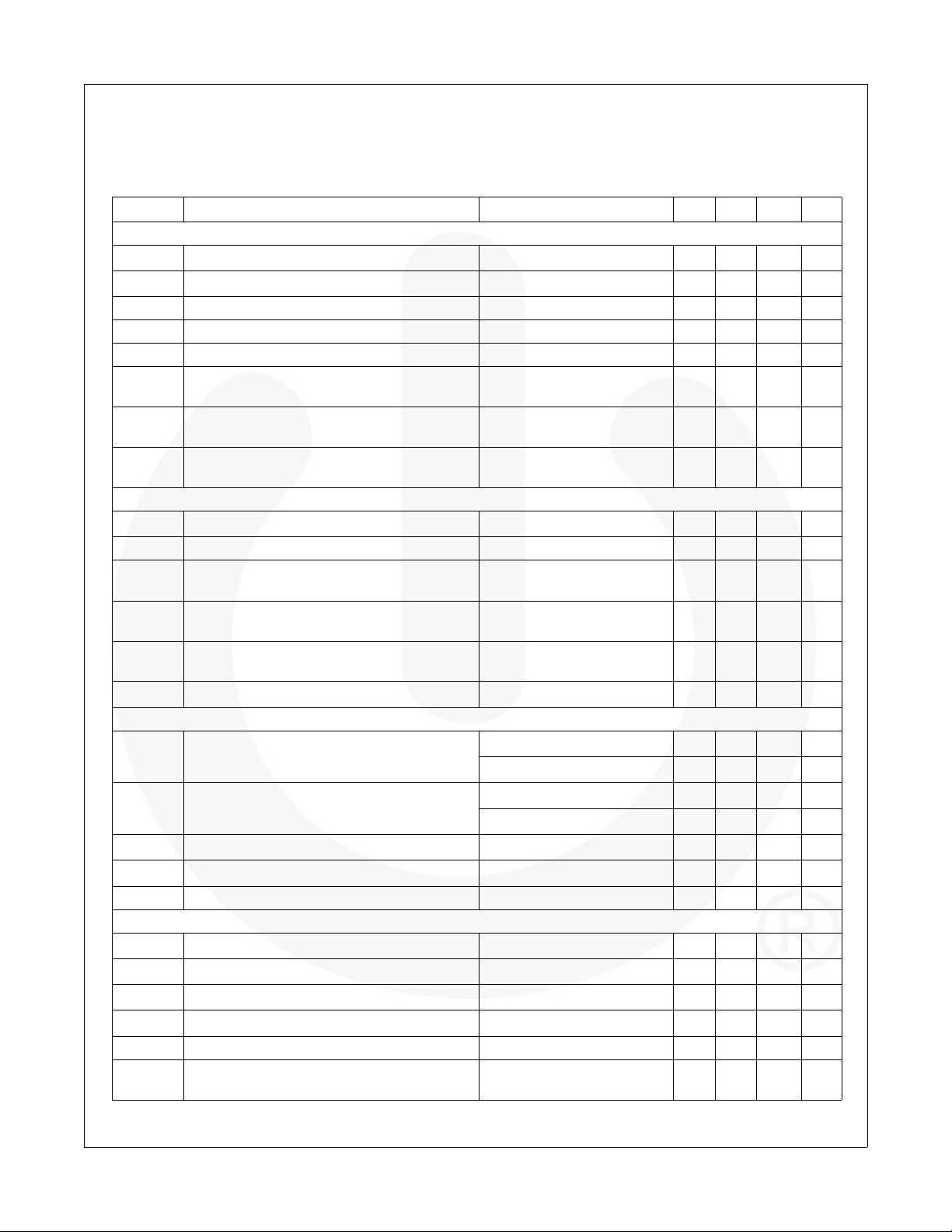
The Recommended Operating Conditions table defines the conditions for actual device operation. Recommended
operating conditions are specified to ensure optimal perfor mance to the datasheet specifications. Fairchild does not
recommend exceeding them or designing to absolute maximum ratings.
Symbol Parameter Min. Max. Unit
V
B
V
S
V
HO
V
CC
V
LO
V
DD
V
SS
V
IN
T
A
© 2009 Fairchild Semiconductor Corporation www.fairchildsemi.com
FAN7392 Rev. 1.0.4 5
High-Side Floating Supply Voltage VS+10 VS+20 V
High-Side Floating Supply Offset Voltage 6-V
High-Side Output Voltage V
CC
S
600 V
V
B
V
Low-Side Supply Voltage 10 20 V
Low-Side Output Voltage 0 V
CC
V
Logic Supply Voltage VSS+3 VSS+20 V
Logic Supply Offset Voltage -5 5 V
Logic Input Voltage V
SS
V
DD
V
Operating Ambient Temperature -40 +125 C
Electrical Characteristics
V
BIAS(VCC
parameters are referenced to VSS and are applicable to the respective input leads: HIN, LIN, and SD. The VO and I
parameters are referenced to VS and COM and are applicable to the respective output leads: HO and LO.
Symbol Characteristics Test Condition Min. Typ. Max. Unit
Low-Side Power Supply Section
V
V
V
Bootstrapped Supply Section
V
V
V
Input Locic Section (HIN, LIN, and SD)
Gate Driver Output Section
VSS/COM VSS-COM/COM-VSS Voltage Endurability -5.0 5.0 V
, VBS, VDD)=15.0V, VSS=COM=0V and TA=25°C, unless otherwise specified. The VIH, VIL, and I
I
QCC
I
QDD
I
PCC
I
PDD
I
SD
CCUV+
CCUV-
CCUVH
I
QBS
I
PBS
BSUV+
BSUV-
BSUVH
I
LK
V
IH
Quiescent VCC Supply Current
Quiescent VDD Supply Current
Operating VCC Supply Current fIN=20kHz, rms, VIN=15V
Operating VDD Supply Current fIN=20kHz, rms, VIN=15V
Shutdown Supply Current SD=V
VCC Supply Under-Voltage
Positive-Going Threshold Voltage
VCC Supply Under-Voltage
Negative-Going Threshold Voltage
VCC Supply Under-Voltage Lockout
Hysteresis Voltage
Quiescent VBS Supply Current
Operating VBS Supply Current fIN=20kHz, rms value 500 A
VBS Supply Under-Voltage
Positive-Going Threshold Voltage
VBS Supply Under-Voltage
Negative-Going Threshold Voltage
VBS Supply Under-Voltage Lockout
Hysteresis Voltage
Offset Supply Leakage Current
Logic “1” Input Threshold Voltage
VIN=0V or V
VIN=0V or V
DD
DD
DD
VIN=0V, VCC=Sweep
VIN=0V, VCC=Sweep
VIN=0V, VCC=Sweep
VIN=0V or V
DD
VIN=0V, VBS=Sweep
VIN=0V, VBS=Sweep
VIN=0V, VBS=Sweep
VB=VS=600V
VDD=3V
VDD=15V
PP
PP
430 A
300 A
120 A
7.7 8.8 9.9 V
7.3 8.4 9.5 V
0.4 V
7.7 8.8 9.9 V
7.3 8.4 9.5 V
0.4 V
2.4 V
9.5 V
40 80 A
60 130 A
VDD=3V
V
I
IN+
I
R
V
V
I
I
- V
IN-
OH
OL
O+
O-
Logic “0” Input Threshold Voltage
IL
Logic Input High Bias Current
Logic Input Low Bias Current
Logic Input Pull-Down Resistance 375 750 K
IN
High-Level Output Voltage (V
BIAS
- VO)
Low-Level Output Voltage
Output High, Short-Circuit Pulsed Current
Output Low, Short-Circuit Pulsed Current
Allowable Negative VS Pin Voltage for HIN
S
Signal Propagation to HO
VDD=15V
VIN=V
VIN=0V
No Load (IO=0A)
No Load (IO=0A)
(4)
VO=0V, PW 10µs
(4)
VO=15V, PW 10µs
DD
20 40 A
2.5 3.0 A
2.5 3.0 A
-9.8 -7.0 V
10 A
50 A
0.8 V
4.5 V
3 A
1.5 V
200 mV
FAN7392 — High-Current, High- and Low-Side, Gate-Drive IC
IN
O
© 2009 Fairchild Semiconductor Corporation www.fairchildsemi.com
FAN7392 Rev. 1.0.4 6
 Loading...