

Fairchild FAN73892 service manual
FAN73892
3-Phase Half-Bridge Gate-Drive IC
FAN73892 — 3-Phase Half-Bridge Gate-Drive IC
March 2012
Features
Floating Channel for Bootstrap Operation to +600V
Typically 350mA/650mA Sourcing/Sinking Current-
Driving Capability for All Channels
Extended Allowable Negative V
Signal Propagation at V
DD=VBS
Swing to -9.8V for
S
=15V
Outputs Out of Phase with Input Signals
Over-Current Shutdown Turns Off All Six Drivers
Matched Propagation Delay for All Channels
3.3V and 5V Input Logic Compatible
Adjustable Fault-Clear Timing
Built-in Advanced Input Filter
Built-in Shoot-Through Prevention Logic
Built-in Soft Turn-Off Function
Common-Mode dv/dt Noise-Canceling Circuit
Built-in UVLO Functions for All Channels
Applications
3-Phase Motor Inverter Driver
Air Conditioner, Washing Machine, Refrigerator,
Dish Washer
Industrial Inverter – Sewing Machine, Power Tool
General-Purpose Three-Phase Inverter
Description
The FAN73892 is a monolithic three-phase half-bridge
gate-drive IC designed for high-voltage, high-speed,
driving MOSFETs and IGBTs operating up to +600V.
Fairchild’s high-voltage process and common-mode
noise-canceling technique provide stable operation of
high-side drivers under high-dv/dt noise circumstances.
An advanced level-shift circuit allows high-side gate
driver operation up to V
The protection functions include under-voltage lockout
and inverter over-current trip with an automatic faultclear function. Over-current protection that terminates all
six outputs can be derived from an external currentsense resistor. An open-drain fault signal is provided to
indicate that an over-current or under-voltage shutdown
has occurred. The UVLO circuits prevent malfunction
when VDD and VBS are lower than the threshold voltage.
Output drivers typically source and sink 350mA and
650mA, respectively; which is suitable for three-phase
half-bridge applications in motor drive systems.
= -9.8V (typical) for VBS =15V.
S
28-SOIC
Ordering Information
Part Number Package Operating Temperature Packing Method
FAN73892MX
Note:
1. These devices passed wave-soldering test by JESD22A-111.
© 2011 Fairchild Semiconductor Corporation www.fairchildsemi.com
FAN73892 • Rev.1.0.1
(1)
28-SOIC -40 to +125°C Tape & Reel
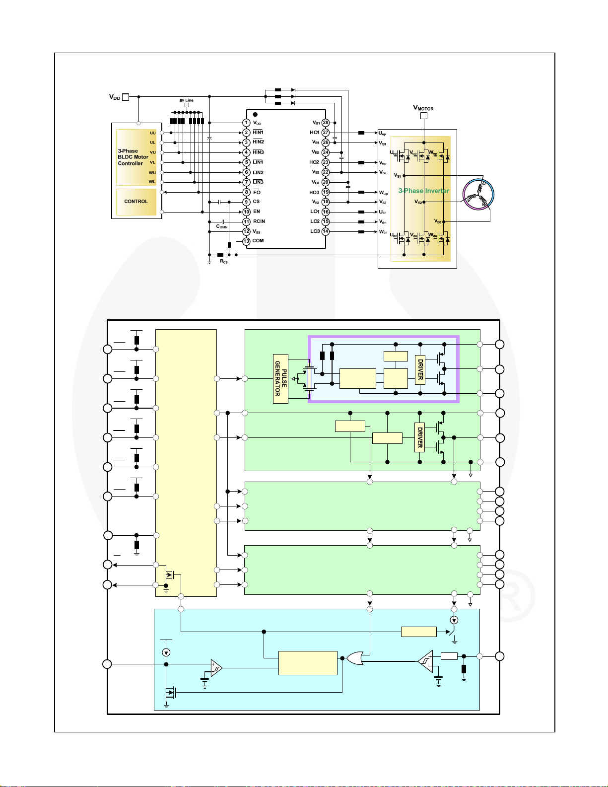
Typical Application Diagram
Figure 1. 3-Phase BLDC Motor Drive Application
Internal Block Diagram
FAN73892 — 3-Phase Half-Bridge Gate-Drive IC
FAN73892M
I
SOFT
I
SOFT
V
HO1
V
V
LO1
COM
V
HO2
V
LO2
V
HO3
V
LO3
B1
S1
DD
B2
S2
B3
S3
28
27
26
1
16
13
24
23
22
15
COM
20
19
18
14
2
50K
HIN2
3
HIN3
4
LIN1
5
LIN2
6
LIN3
7
INPUT NOISE
50K
[ t
FLTIN
50K
SHOOT-THROUGH
50K
PREVENTION
DEAD-TIME
50K
[ D
FILTER
=250ns ]
=300ns ]
T
UHIN
V
DD
ULIN
U Phase Driver
V
DD
VHIN
ENABLE INPUT
EN
10
8
12
150K
FO
Vss
[ t
FILTER
FLTEN
=250ns ]
VLIN
V
DD
WHIN
WLIN
NOISE
CANCELLER
UVLO
V Phase Driver
W Phase Driver
UVLO
R
S
DELAY
R
Q
50K
HIN1
COM
V
DD_UVLO
Fault
V
REF
i
RCIN
11
RCIN
V
RCIN,TH
V
RCIN,HYS
= 3.3V
= 0.7V
Q
R
SET
DOMINANT
LATCH
S
SOFT-OFF
CS_COMP
3.3V
LEB
0.5V
I
SOFT
CS
9
Protection Circuit
Figure 2. Functional Block Diagram
© 2011 Fairchild Semiconductor Corporation www.fairchildsemi.com
FAN73892 • Rev.1.0.1 2
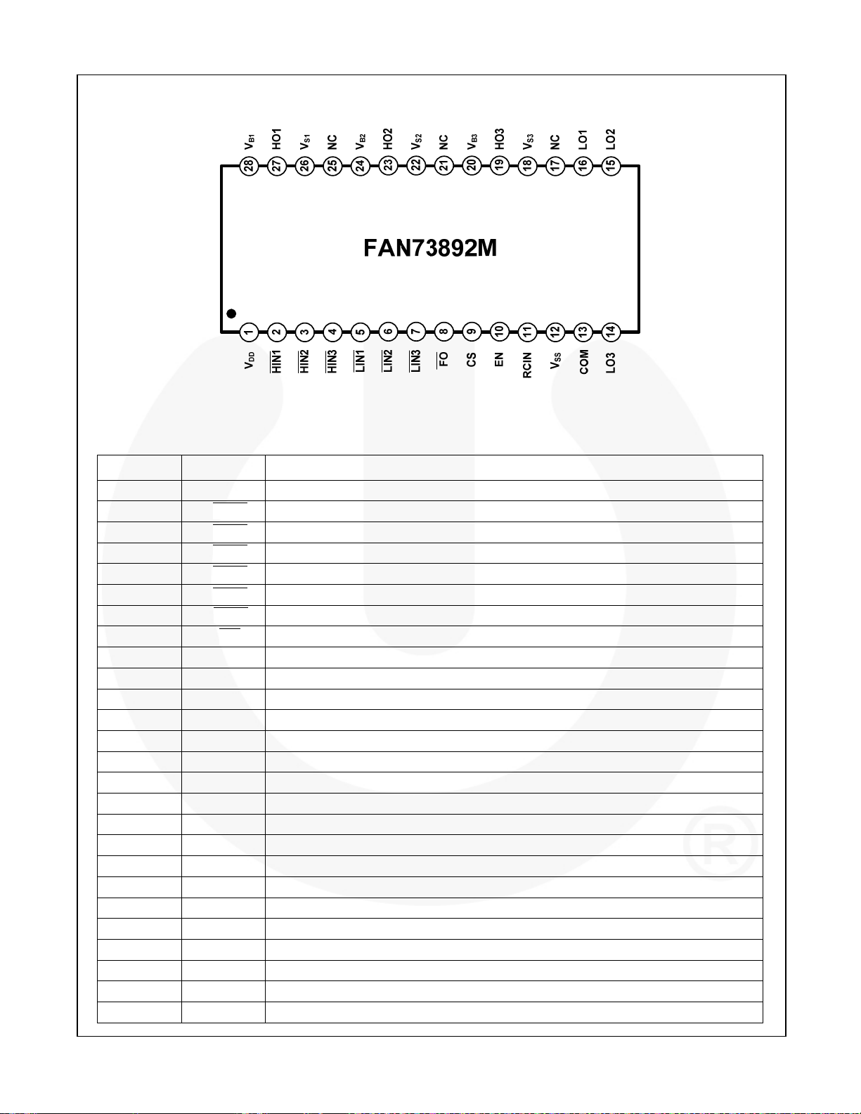
Pin Configuration
Pin Definitions
FAN73892 — 3-Phase Half-Bridge Gate-Drive IC
Figure 3. Pin Assignments
Pin Name Description
1 V
2 Logic Input 1 for high-side gate 1 driver
3 Logic Input 2 for high-side gate 2 driver
4 Logic Input 3 for high-side gate 3 driver
5 Logic Input 1 for low-side gate 1 driver
6 Logic Input 2 for low-side gate 2 driver
7 Logic Input 3 for low-side gate 3 driver
8 Fault output with open drain (indicates over-current and low-side under-voltage)
9 CS Analog input for over-current shutdown
10 EN Logic input for shutdown functionality
11 RCIN An external RC network input used to define the fault-clear delay
12 VSS Logic ground
13 COM Low-side driver return
14 LO3 Low-side gate driver 3 output
15 LO2 Low-side gate driver 2 output
16 LO1 Low-side gate driver 1 output
17, 21, 25 NC No connect
18 VS3 High-side driver 3 floating supply offset voltage
19 HO3 High-side driver 3 gate driver output
20 VB3 High-side driver 3 floating supply
22 VS2 High-side driver 2 floating supply offset voltage
23 HO2 High-side driver 2 gate driver output
24 VB2 High-side driver 2 floating supply
26 VS1 High-side driver 1 floating supply offset voltage
27 HO1 High-side driver 1 gate driver output
28 VB1 High-side driver 1 floating supply
DD
HIN1
HIN2
HIN3
LIN1
LIN2
LIN3
FO
Logic and low-side gate driver power supply voltage
© 2011 Fairchild Semiconductor Corporation www.fairchildsemi.com
FAN73892 • Rev.1.0.1 3
FAN73892 — 3-Phase Half-Bridge Gate-Drive IC
Absolute Maximum Ratings
Stresses exceeding the Absolute Maximum Ratings may damage the device. The device may not function or be
operable above the recommended operating conditions and stressing the parts to these levels is not recommended.
In addition, extended exposure to stresses above the recommended operating conditions may affect device reliability.
The absolute maximum ratings are stress ratings only. T
Symbol Parameter Min. Max. Unit
VS High-Side Floating Offset Voltage V
VB High-Side Floating Supply Voltage -0.3 625.0 V
VDD Low-Side and Logic-Fixed supply voltage -0.3 25.0 V
VHO High-Side Floating Output Voltage V
VLO Low-Side Floating Output Voltage V
VIN Input Voltage ( , , CS, and EN) -0.3 5.5 V
VFO Fault Output Voltage ( ) -0.3 VDD+0.3 V
PW
High-Side Input Pulse Width 500 ns
HIN
dVS/dt Allowable Offset Voltage Slew Rate ±50 V/ns
PD Power Dissipation
θJA Thermal Resistance 70 °C/W
TJ Junction Temperature 150 °C
T
Storage Temperature -55 150 °C
STG
Notes:
2. Mounted on 76.2 x 114.3 x 1.6mm PCB (FR-4 glass epoxy material). Refe r to the following standards:
JESD51-2: Integral circuit’s thermal test method environmental conditions, natural convection;
JESD51-3: Low effective thermal conductivity test board for leaded surface-mount packages.
3. Do not exceed maximum power dissipation (P
HINx
LINx
FO
(2,2)
1.4 W
=25°C, unless otherwise specified.
A
V
HO1,2,3
-0.3 VDD+0.3 V
LO1,2,3
) under any circumstances.
D
B1,2,3
S1,2,3
-25 V
-0.3 V
+0.3 V
B1,2,3
+0.3 V
B1,2,3
Recommended Operating Conditions
The Recommended Operating Conditions table defines the conditions for actual device operation. Recommended
operating conditions are specified to ensure optimal performance to the datasheet specifications. Fairchild does not
recommend exceeding them or designing to Absolute Maximum Ratings.
Symbol Parameter Min. Max. Unit
V
High-Side Floating Supply Voltage V
B1,2,3
V
High-Side Floating Supply Offset Voltage 6-VDD 600 V
S1,2,3
VDD Low-Side and Logic Fixed Supply Voltage 10 20 V
V
High-Side Output Voltage V
HO1,2,3
V
Low-Side Output Voltage COM VDD V
LO1,2,3
VFO Fault Output Voltage ( ) VSS V
FO
VCS Current-Sense Pin Input Voltage VSS 5 V
VIN Logic Input Voltage ( and ) VSS 5 V
HIN1,2,3
LIN1,2,3
VSS Logic Ground -5 5 V
TA Ambient Temperature -40 +125 °C
S1,2,3
S1,2,3
+10 V
V
+20 V
S1,2,3
V
B1,2,3
V
DD
© 2011 Fairchild Semiconductor Corporation www.fairchildsemi.com
FAN73892 • Rev.1.0.1 4
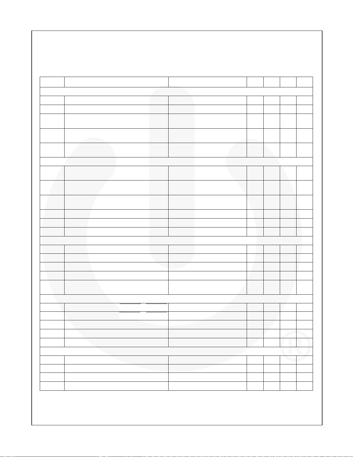
Electrical Characteristics
V
BIAS (VDD
COM and are applicable to all six channels. The V
applicable to the respective output leads: HO1,2,3 and LO1,2,3. The V
V
BSUV
Symbol Parameter Condition Min. Typ. Max. Unit
Low-Side Power Supply Section
V
V
V
Bootstrapped Power Supply Section
V
V
V
Gate Driver Output Section
Logic Input Section
Enable Control Section (EN)
V
, V
parameters are referenced to V
I
Quiescent VDD Supply Current V
QDD
I
Operating VDD Supply Current f
PDD
DDUV+
DDUV-
DDHYS
BSUV+
BSUV-
BSHYS
ILK Offset Supply Leakage Current V
I
Quiescent VBS Supply Current V
QBS
I
Operating VBS Supply Current f
PBS
VOH High-Level Output voltage, V
VOL Low-Level Output voltage, VO I
IO+ Output HIGH Short-Circuit Pulse Current
IO- Output LOW Short-Circuit Pulsed Current
VS
VIH Logic "0" Input Voltage , 2.5 V
VIL Logic "1" Input Voltage , 0.8 V
I
IN+
I
IN-
RIN
EN+
V
EN-
I
EN+
I
EN-
) = 15.0V and TA = 25°C unless otherwise specified. The VIN and IIN parameters are referenced to
BS1,2,3
.
S1,2,3
VDD Supply Under-Voltage Positive-Going
Threshold
V
Supply Under-Voltage Negative-Going
DD
Threshold
VDD Supply Under-Voltage Lockout
Hysteresis
VBS Supply Under-Voltage Positive-Going
Threshold
VBS Supply Under-Voltage Negative-Going
Threshold
VBS Supply Under-Voltage Lockout
Hysteresis
BIAS-VO
Allowable Negative VS Pin Voltage for HIN
Signal Propagation to HO
and IO parameters are referenced to V
O
=0V or 5V, EN=0V 200
LIN1,2,3
=20kHz, rms Value 500
LIN1,2,3
parameters are referenced to COM. The
DDUV
VDD=Sweep 7.5 8.5 9.3 V
=Sweep 7.0 8.0 8.7 V
V
DD
VDD=Sweep 0.5 V
V
=Sweep 7.5 8.5 9.3 V
BS1,2,3
V
=Sweep 7.0 8.0 8.7 V
BS1,2,3
V
=Sweep 0.5 V
BS1,2,3
B1,2,3=VS1,2,3
HIN1,2,3
HIN1,2,3
I
=0mA (No Load) 100 mV
O
=0mA (No Load) 100 mV
O
(4)
V
=15V, VIN=0V with PW≤10µs
O
(4)
VO=0V, VIN=5V with PW≤10µs
=600V 10
=0V or 5V, EN=0V 10 50 80
=20kHz, rms Value 200 320 480
-9.8 -7.0 V
and COM and are
S1,2,3
μA
μA
μA
μA
μA
250 350 mA
500 650 mA
HIN1,2,3 LIN1,2,3
HIN1,2,3
Logic Input Bias Current (HO=LO=HIGH)
Logic Input Bias Current (HO=LO=LOW)
Logic Input Pull-Up Resistance
LIN1,2,3
VIN=0V 100
VIN=5V 8.5 25
50
μA
μA
KΩ
Enable Positive-Going Threshold Voltage 2.5 V
Enable Negative-Going Threshold Voltage 0.8 V
Logic Enable “1” Input Bias Current
Logic Enable “0” Input Bias Current
=5V (Pull-Down=150KΩ)
V
EN
VEN=0V 2
33
μA
μA
FAN73892 — 3-Phase Half-Bridge Gate-Drive IC
Continued on the following page…
© 2011 Fairchild Semiconductor Corporation www.fairchildsemi.com
FAN73892 • Rev.1.0.1 5
 Loading...