Fairchild FAN7382 service manual
FAN7382
Half-Bridge Gate-Driver IC
FAN7382 Half-Bridge Gate-Driver IC
October 2006
Features
Floating Channels Designed for Bootstrap Operation
to +600V
Typically 350mA/650mA Sourcing/Sinking Current
Driving Capability for Both Channels
Common-Mode dv/dt Noise Canceling Circuit
Extended Allowable Negative V
nal Propagation at VCC=VBS=15V
V
& VBS Supply Range from 10V to 20V
CC
UVLO Functions for Both Channels
TTL Compatible Input Logic Threshold Levels
Matched Propagation Delay Below 50nsec
Output In-phase with Input
Swing to -9V for Sig-
S
Applications
PDP Scan Driver
Fluorescent Lamp Ballast
SMPS
Motor Driver
Description
The FAN7382, a monolithic half-bridge gate-driver IC,
can drive MOSFETs and IGBTs that operate up to
+600V. Fairchild’s high-voltage process and commonmode noise canceling technique provides stable operation of the high-side driver under high-dv/dt noise circumstances. An advanced level-shift circuit allows high-side
gate driver operation up to V
VBS=15V. The input logic level is compatible with standard TTL-series logic gates. UVLO circuits for both channels prevent malfunction when V
the specified threshold voltage. Output drivers typically
source/sink 350mA/650mA, respectively, which is suitable for fluorescent lamp ballasts, PDP scan drivers,
motor controls, etc.
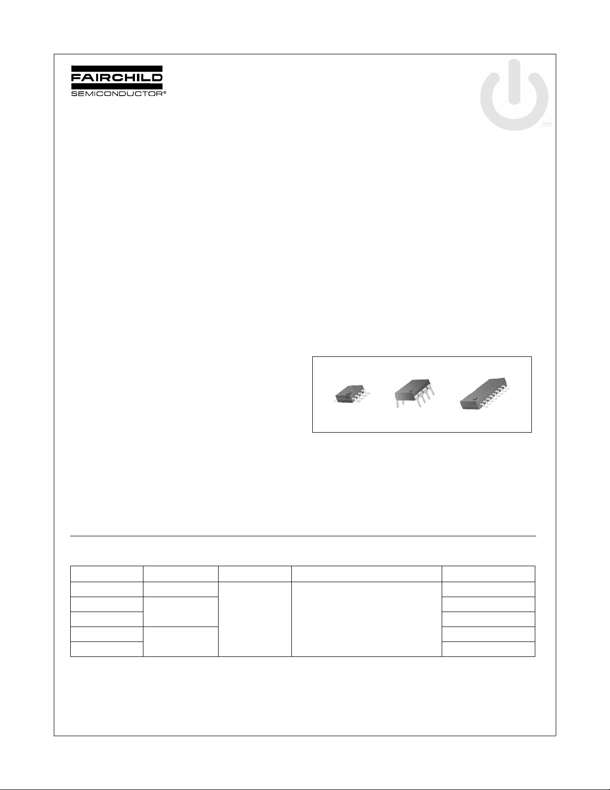
8-SOP
8-DIP
=-9.8V (typical) for
S
or VBS is lower than
CC
14-SOP
Ordering Information
Part Number Package Pb-Free Operating Temperature Range Packing Method
FAN7382N 8-DIP
FAN7382M
FAN7382MX
FAN7382M1
FAN7382M1X Tape & Reel
Note:
1. These devices passed wave soldering test by JESD22A-111.
© 2005 Fairchild Semiconductor Corporation www.fairchildsemi.com
FAN7382 Rev. 1.0.6
(1)
(1)
8-SOP
14-SOP
Yes -40°C ~ 125°C
Tube
Tube
Tape & Reel
Tube
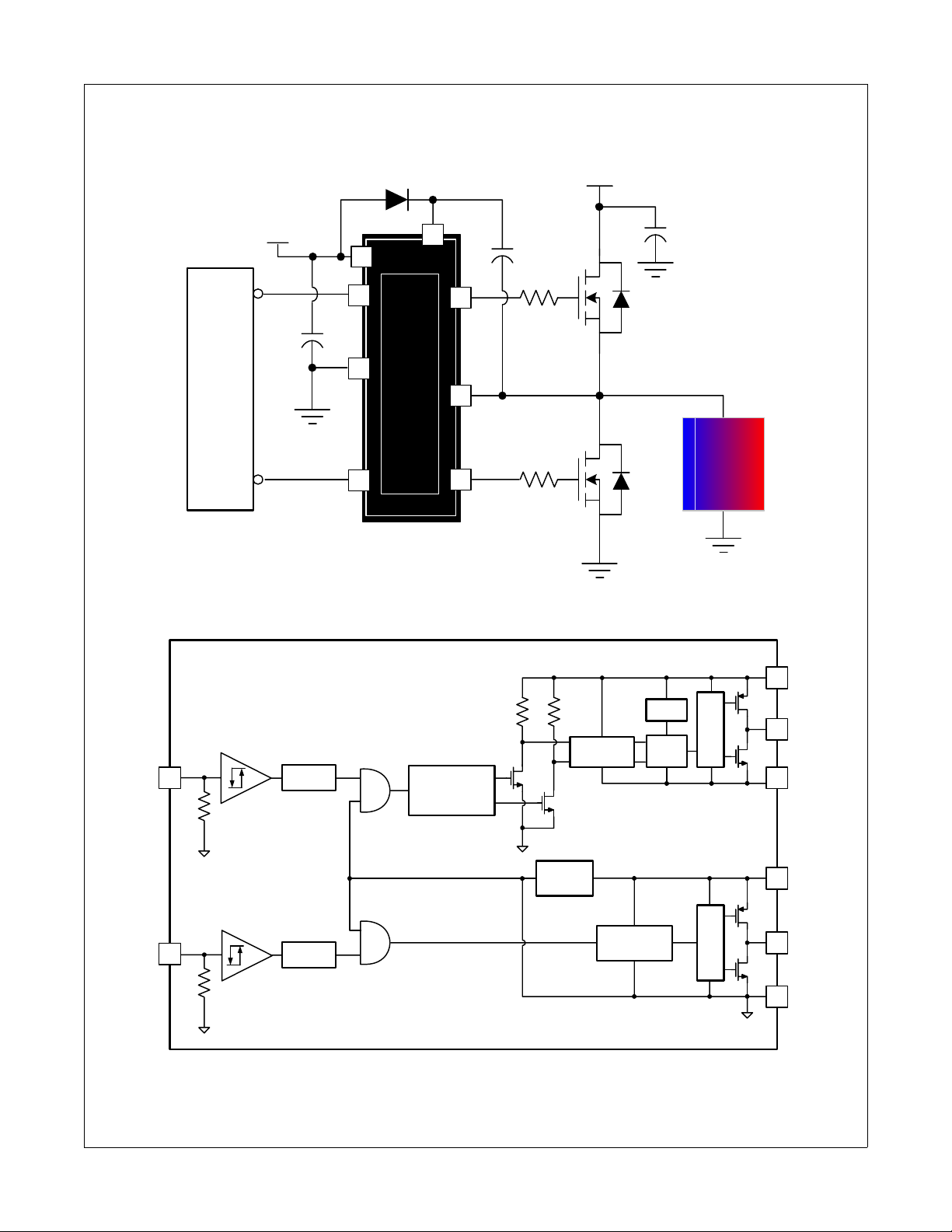
Typical Application Circuit
FAN7382 Half-Bridge Gate-Driver IC
CONTROLLR
ON / OFF
DB
V
V
CC
B
8
1
V
CC
2
HIN
7
HO
C
BS
Up to 600V
FAN7382
4
COM
3
LIN
6
V
S
LOAD
5
LO
FAN7382 Rev.04
Internal Block Diagram
HIN
500kΩ
LIN
500kΩ
DELAY
DELAY
SHIFTER
PULSE
GENERATION
LEVEL
CANCELLER
UVLO
HIGH-SIDE DRIVER
UVLO
NOISE
RSR
Q
LOW-SIDE DRIVER
DELAY
DRIVER DRIVER
i
FAN7382 Rev.03
V
B
HO
V
S
V
CC
LO
COM
© 2005 Fairchild Semiconductor Corporation www.fairchildsemi.com
FAN7382 Rev. 1.0.6 2
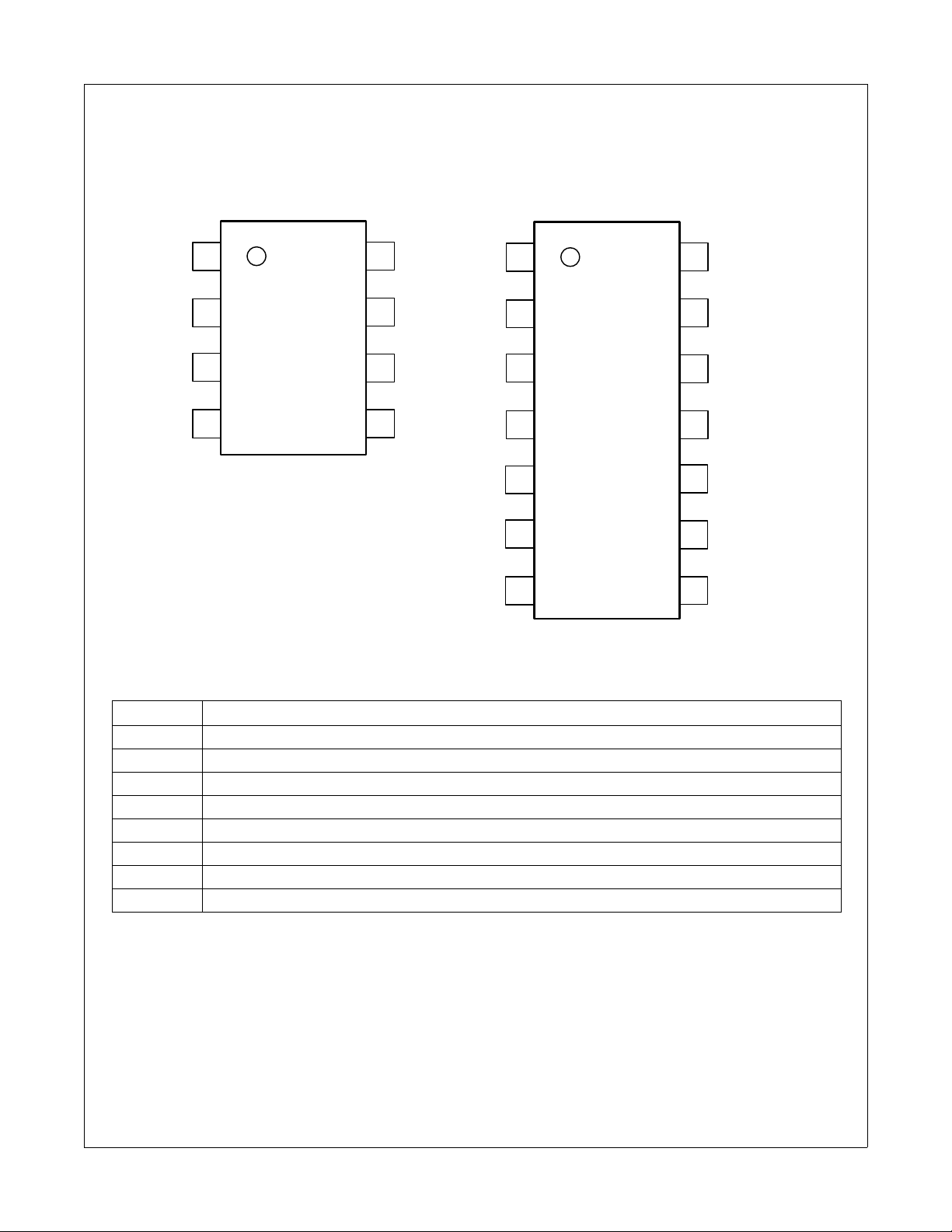
Pin Assignments
FAN7382 Half-Bridge Gate-Driver IC
FAN7382N
FAN7382M FAN7382M1
1
V
CC
HIN
2
3
LIN
COM
4
Pin Definitions
FAN7382 Rev.04
V
8
B
HO
7
V
6
S
LO
5
1 14
V
CC
HIN
2
3
LIN
4
NC
NC
5
6
COM
LO
7
FAN7382 Rev.00
13
12
11
10
NC
V
B
HO
V
S
NC
NC
9
NC
8
Name Description
V
CC
HIN Logic Input for High-Side Gate Driver Output
LIN Logic Input for Low-Side Gate Driver Output
COM Logic Ground and Low-Side Driver Return
LO Low-Side Driver Output
V
S
HO High-Side Driver Output
V
B
© 2005 Fairchild Semiconductor Corporation www.fairchildsemi.com
FAN7382 Rev. 1.0.6 3
Low-Side Supply Voltage
High-Voltage Floating Supply Return
High-Side Floating Supply
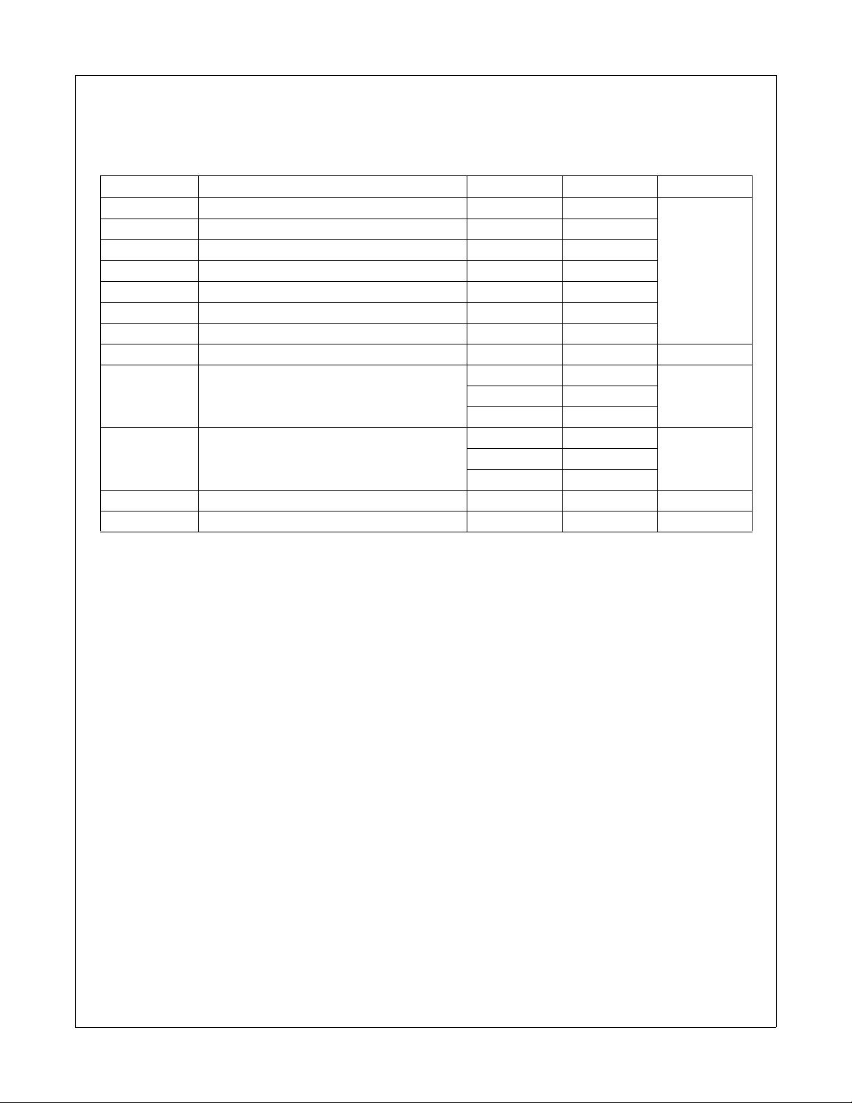
Absolute Maximum Ratings
The “Absolute Maximum Ratings” are those values beyond wh ich the safety o f the device cannot be guaranteed. The
device should not be operated at these limits. The parametric values defined in the Electrical Characteristics tables
are not guaranteed at the absolute maximum ratings.
Symbol Characteristics Min. Max. Unit
V
S
V
B
V
HO
V
CC
V
LO
V
IN
COM Logic ground V
/dt Allowable offset voltage slew rate 50 V/nsec
dV
S
P
D
θ
JA
T
J
T
STG
High-side offset voltage VB-25 VB+0.3
High-side floating supply voltage -0.3 625
High-side floating output voltage HO VS-0.3 VB+0.3
Low-side and logic fixed supply voltage -0.3 25
V
Low-side output voltage LO -0.3 VCC+0.3
Logic input voltage (HIN, LIN) -0.3 VCC+0.3
-25 VCC+0.3
CC
8-SOP 0.625
Power dissipation
W14-SOP 1.0
8-DIP 1.2
8-SOP 200
Thermal resistance, junction-to-ambient
°C/W14-SOP 110
8-DIP 100
Junction temperature 150 °C
Storage temperature 150 °C
FAN7382 Half-Bridge Gate-Driver IC
© 2005 Fairchild Semiconductor Corporation www.fairchildsemi.com
FAN7382 Rev. 1.0.6 4
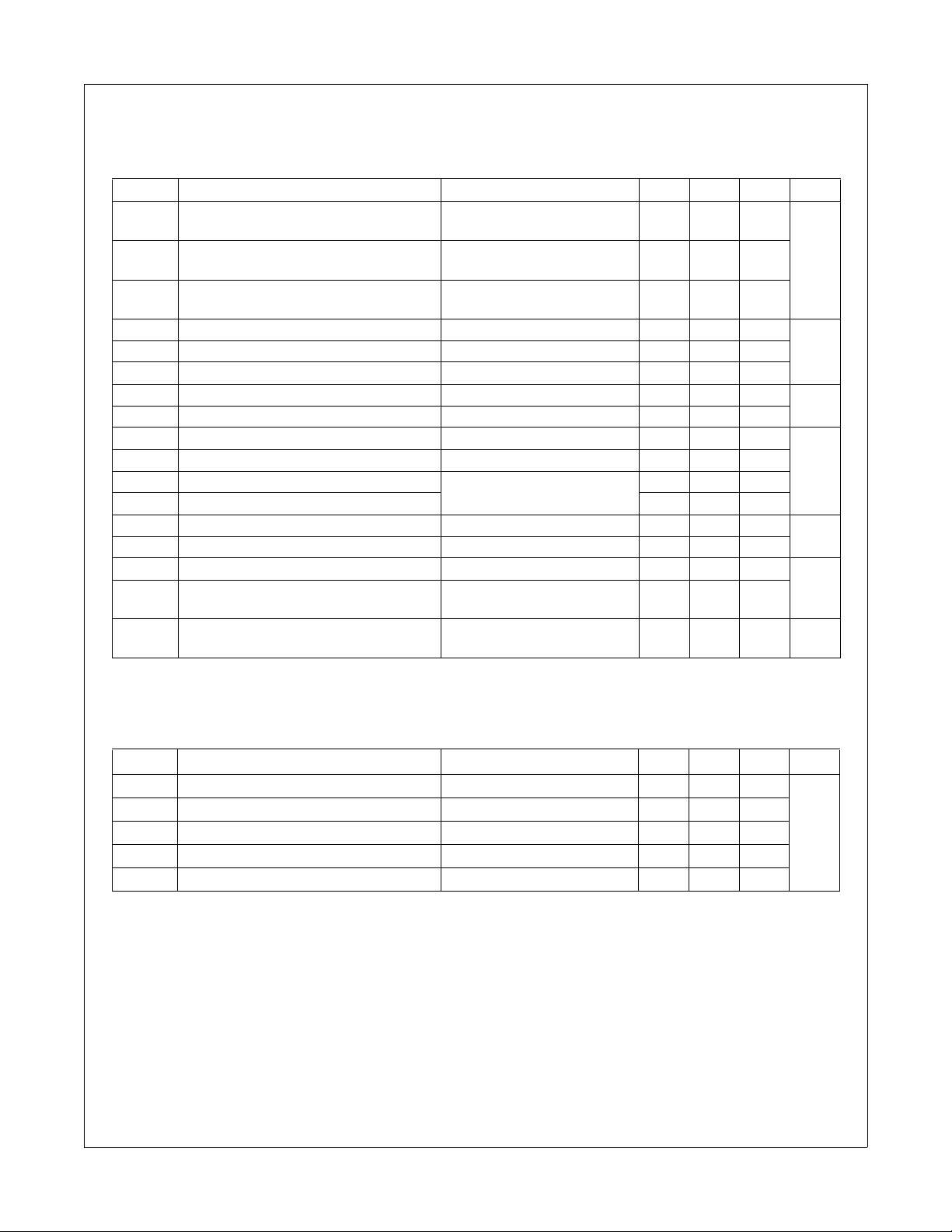
Electrical Characteristics
V
BIAS (VCC
COM. The VO and IO parameters are referenced to COM and VS is applicable to HO and LO.
Symbol Characteristics Test Condition Min. Typ. Max. Unit
V
CCUV+
V
BSUV+
V
CCUV-
V
BSUV-
V
CCUVH
V
BSUVH
I
I
I
V
V
, VBS)=15.0V, TA = 25°C, unless otherwise specified. The VIN, VTH, and IIN parameters are referenced to
I
LK
QBS
QCC
PBS
PCC
V
IH
V
IL
OH
OL
I
IN+
I
IN-
I
O+
I
O-
V
S
VCC and VBS supply under-voltage
positive going threshold
VCC and VBS supply under-voltage
negative going threshold
VCC supply under-voltage lockout
hysteresis
Offset supply leakage current VB=VS=600V 50
Quiescent VBS supply current VIN=0V or 5V 45 120
Quiescent VCC supply current VIN=0V or 5V 70 180
Operating VBS supply current fIN=20kHz,rms value 600
Operating VCC supply current fIN=20kHz,rms value 600
Logic "1" input voltage 2.9
Logic "0" input voltage 0.8
High-level output voltage, V
Low-level output voltage, V
BIAS-VO
O
IO=20mA
Logic "1" input bias current VIN=5V 10 20
Logic "0" input bias current VIN=0V 1.0 2.0
Output high short-circuit pulsed current VO=0V,VIN=5V with PW<10µs 250 350
Output low short-circuit pulsed current VO=15V=VB,VIN=0V with
PW<10µs
Allowable negative VS pin voltage for
HIN signal propagation to HO
8.2 9.2 10.0
7.6 8.7 9.6
0.6
500 650
-9.8 -7.0 V
µAI
µA
1.0
0.6
µA
mA
FAN7382 Half-Bridge Gate-Driver IC
V
V
Dynamic Electrical Characteristics
V
BIAS (VCC
Symbol Characteristics Test Condition Min. Typ. Max. Unit
© 2005 Fairchild Semiconductor Corporation www.fairchildsemi.com
FAN7382 Rev. 1.0.6 5
, VBS)=15.0V, VS=COM, CL=1000pF and, TA = 25°C, unless otherwise specified.
t
t
Turn-on propagation delay VS=0V 100 170 300
on
Turn-off propagation delay VS=0V or 600V 100 200 300
off
Turn-on rise time 20 60 140
t
r
Turn-off fall time 30 80
t
f
MT Delay matching, HS & LS turn-on/off 50
nsec
 Loading...