FAN7171_F085
8-SOP
High-Current High-Side Gate Drive IC
FAN7171_F085 — High-Current High-Side Gate Drive IC
October 2011
Features
Floating Channel for Bootstrap Operation to +600V
4A/4A Sourcing/Sinking Current Driving Capability
Common-Mode dv/dt Noise Canceling Circuit
3.3V and 5V Input Logic Compatible
Output In-phase with Input Signal
Under- Voltage Lockout for V
25V Shunt Regulator on V
8-Lead Small Outline Package (SOP)
Qualified to AEC Q100
DD
BS
and V
BS
Applications
High-Speed Gate Driver
High-Power Buck Converter
Motor Drive Inverter
Description
The FAN7171_F085 is a monolithic high-side gate drive
IC, which can drive high-speed MOSFETs and IGBTs
that operate up to +600V. It has a buffered output stage
with all NMOS transistors designed for high pulse current
driving capability and minimum cross-conduction.
Fairchild’s high-voltage process and common-mode
noise canceling techniques provide stable operation of
the high-side driver under high dv/dt noise circumstances. An advanced level-shift circuit offers high-side
gate driver operation up to V
V
=15V.
BS
The UVLO circuit prevents malfunction when V
lower than the specified threshold voltage.
The high-current and low-output voltage drop feature
makes this device suitable for sustaine switch driver and
energy recovery switch driver in the Plasma Display
Panel application, motor drive inverter, switching power
supply, and high-power DC-DC converter applications.
=-9.8V (typical) for
S
BS
is
Ordering Information
Part Number Package
FAN7171M
FAN7171MX
Note:
1. These devices passed wave soldering test by JESD22A-111.
For Fairchild’s definition of “green” Eco Status, please visit: http://www.fairchildsemi.com/company/green/rohs_green.html.
© 2011 Fairchild Semiconductor Corporation www.fairchildsemi.com
FAN7171_F085 Rev. 1.0.0
(1)
(1)
8-SOP -40°C ~ 125°C RoHS
Operating
Temperature Range
Eco Status Packing Method
Tube
Tape & Reel

Typical Application Diagrams
D
BOOT
C2
PWM
C
BOOT
C1
D1
L1
15V
R
BOOT
R2
FAN7171_F805
V
B
IN
GND
HO
V
S
NC
NC
V
DD
7
5
6
8
2
4
3
1
R1
V
IN
V
OUT
UVLO
PULSE
GENERATOR
V
DD
GND
IN
V
B
HO
V
S
R
R
S
Q
6
7
81
4
2
NOISE
CANCELLER
Pins 3 and 5 are no connection.
25V
25V
110K
V
DD
Shoot-through current
compensated gate driver
FAN7171_F085 — High-Current High-Side Gate Drive IC
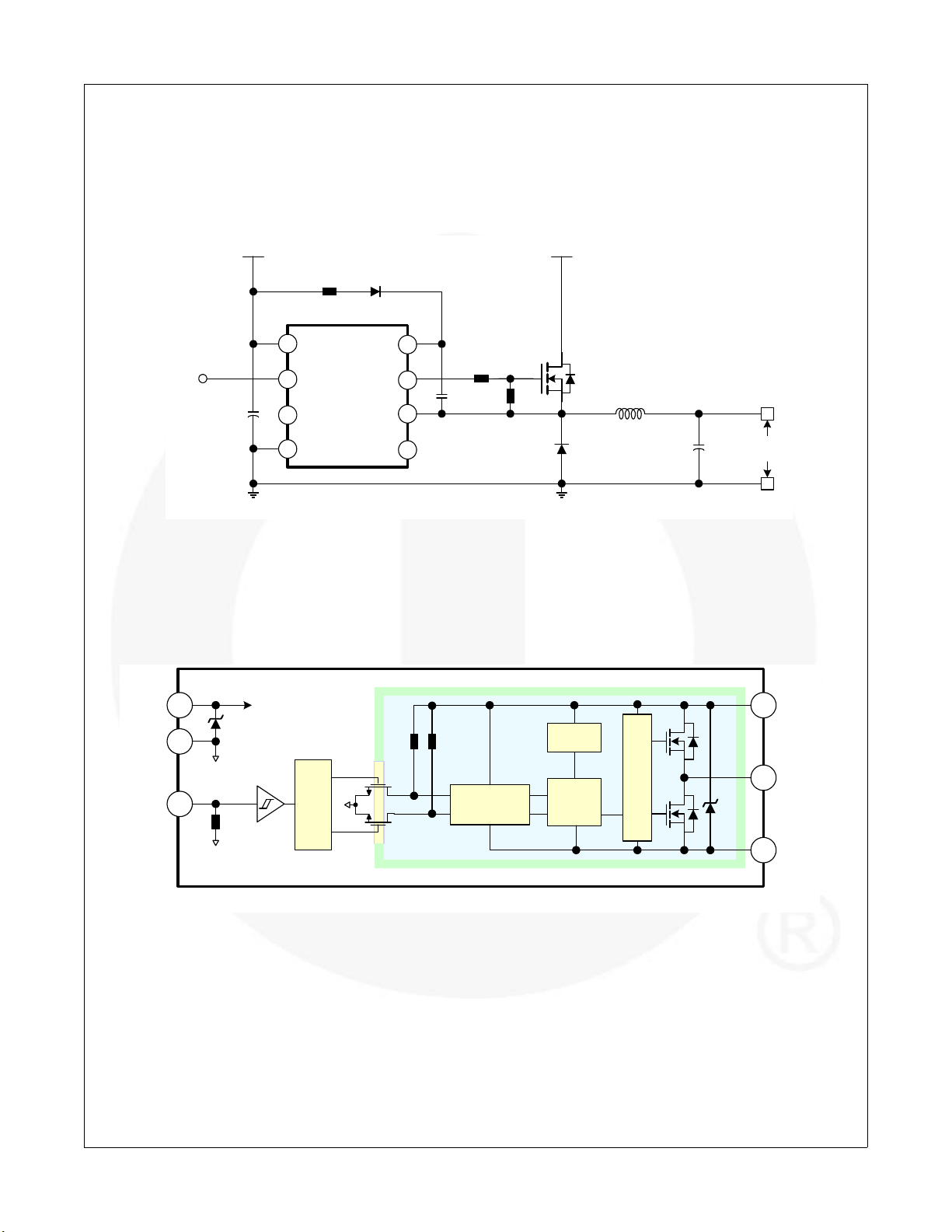
Figure 1. Application Circuit for Step-Down (Buck) DC-DC Converter
© 2011 Fairchild Semiconductor Corporation www.fairchildsemi.com
FAN7171_F085 Rev. 1.0.0 2
Figure 2. Functional Block Diagram

Pin Configuration
V
S
V
B
FAN7371
V
DD
NC
IN HO
NC
4GND
3
2
1
5
6
7
8
FAN7171
_F085
FAN7171_F085 — High-Current High-Side Gate Drive IC
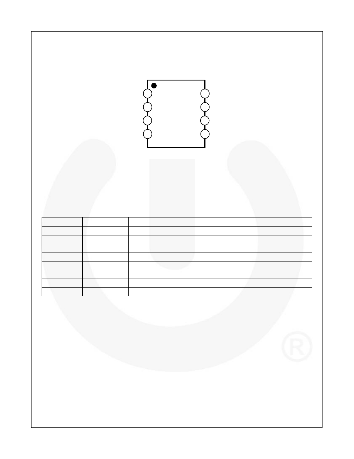
Figure 3. Pin Assignments(Top View)
Pin Definitions
Pin # Name Description
1VDDSupply Voltage
2 IN Logic Input for High-Side Gate Driver Output
3 NC No Connection
4 GND Ground
5 NC No Connection
6V
7 HO High-Side Driver Output
8V
S
B
High-Voltage Floating Supply Return
High-Side Floating Supply
© 2011 Fairchild Semiconductor Corporation www.fairchildsemi.com
FAN7171_F085 Rev. 1.0.0 3

Absolute Maximum Ratings
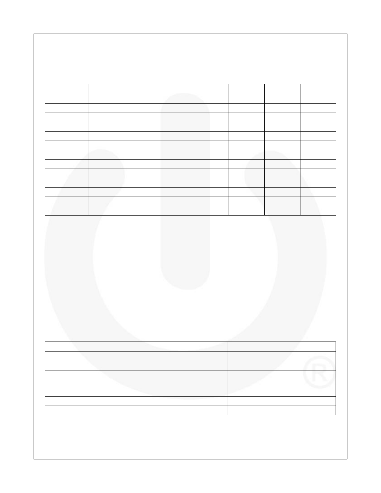
Stresses exceeding the absolute maximum ratings may damage the device. The device may not function or be operable above the recommended operating conditions and stressing the parts to these levels is not recommended. In addition, extended exposure to stresses above the recommended operating conditions may affect device reliability. The
absolute maximum ratings are stress ratings only. -40°C<=T
Symbol Characteristics Min. Max. Unit
V
S
V
B
V
HO
V
DD
V
IN
/dt Allowable Offset Voltage Slew Rate ± 50 V/ns
dV
S
P
D
JA
T
J
T
STG
T
A
V
ESD
V
CDM
Notes:
1) This IC contains a shunt regulator on VDD and VBS with a normal breakdown voltage of 25V. Please note that
this supply pin should not be driven by a low-impedance voltage source greater than the VSHUNT specified in
the Electrical Characteristics section
2) Mounted on 76.2 x 114.3 x 1.6mm PCB (FR-4 glass epoxy material).
3) Refer to the following standards:
JESD51-2: Integral circuits thermal test method environmental conditions, natural convection, and
JESD51-3: Low effective thermal conductivity test board for leaded surface mount packages.
4 Do not exceed power dissipation (P
High-Side Floating Offset Voltage VB-V
High-Side Floating Supply Voltage
(2)
High-Side Floating Output Voltage VS-0.3 VB+0.3 V
Low-Side and Logic Supply Voltage
Logic Input Voltage -0.3 VDD+0.3 V
Power Dissipation
(3, 4, 5)
Thermal Resistance 200 C/W
Junction Temperature -55 150 C
Storage Temperature -55 150 C
Operating Ambient Temperature -40 125 C
Human Body Model(HBM) 1500 V
Charge Device Model 500 V
) under any circumstances.
D
<=125°C unless otherwise specified.
A
SHUNT
-0.3 625.0 V
(2)
-0.3 V
VB+0.3 V
SHUNT
0.625 W
V
FAN7171_F085 — High-Current High-Side Gate Drive IC
Recommended Operating Conditions
The Recommended Operating Conditions table defines the conditions for actual device operation. Recommended
operating conditions are specified to ensure optimal performance to the datasheet specifications. Fairchild does not
recommend exceeding them or designing to absolute maximum ratings.
Symbol Parameter Min. Max. Unit
V
BS
V
S
V
S
V
HO
V
IN
V
DD
© 2011 Fairchild Semiconductor Corporation www.fairchildsemi.com
FAN7171_F085 Rev. 1.0.0 4
High-Side Floating Supply Voltage VS+10 VS+20 V
High-Side Floating Supply Offset Voltage(DC) 6-V
High-Side Floating Supply Offset Voltage(Transient)
High-Side Output Voltage V
DD
-15(~170)
-7(~400)
S
Logic Input Voltage GND V
600 V
600
V
B
DD
Supply Voltage 10 20 V
V
V
V
 Loading...