FAN7085_GF085
High Side Gate Driver with Recharge FET
FAN7085_GF085 High Side Gate Driver with Recharge FET
November 2009
Features
• Qualified to AEC Q100
• Floating channel designed for bootstrap operation fu lly operational up to 300V.
• Tolerance to negative transient voltage on VS pin
• dv/dt immune.
• Gate drive supply range from 4.5V to 20V
• Under-voltage lockout
• CMOS Schmitt-triggered inputs with pull-down and pull-up
• High side output out of phase with input (Inverted input)
• Reset input
• Internal recharge FET for bootstrap refresh
Typical Applications
• Diesel and gasoline injectors/valves
• MOSFET-and IGBT high side driver applications
For Fairchild’s definition of “green” Eco Status, please visit:
http://www.fairchildsemi.com/company/green/rohs_green.html
Description
The FAN7085_GF085 is a high-side gate drive IC with reset
input and built-in recharge FET. It is designed for high voltage
and high speed driving of MOSFET or IGBT, which operates up
to 300V. Fairchild's high-voltage process and common-mode
noise cancellation technique provide stable operation in the
high side driver under high-dV/dt noise circumstances. Logic
input is compatible with standard CMOS outputs. The UVLO circuits prevent from malfunction when VCC and VBS are lower
than the specified threshold voltage. It is available with space
saving SOIC-8 Package. Minimum source and sink current
capability of output driver is 250mA and 250mA. Built-in
recharge FET to refresh bootstrap circuit is very useful for circuit
topology requiring switches on low and high side of load.
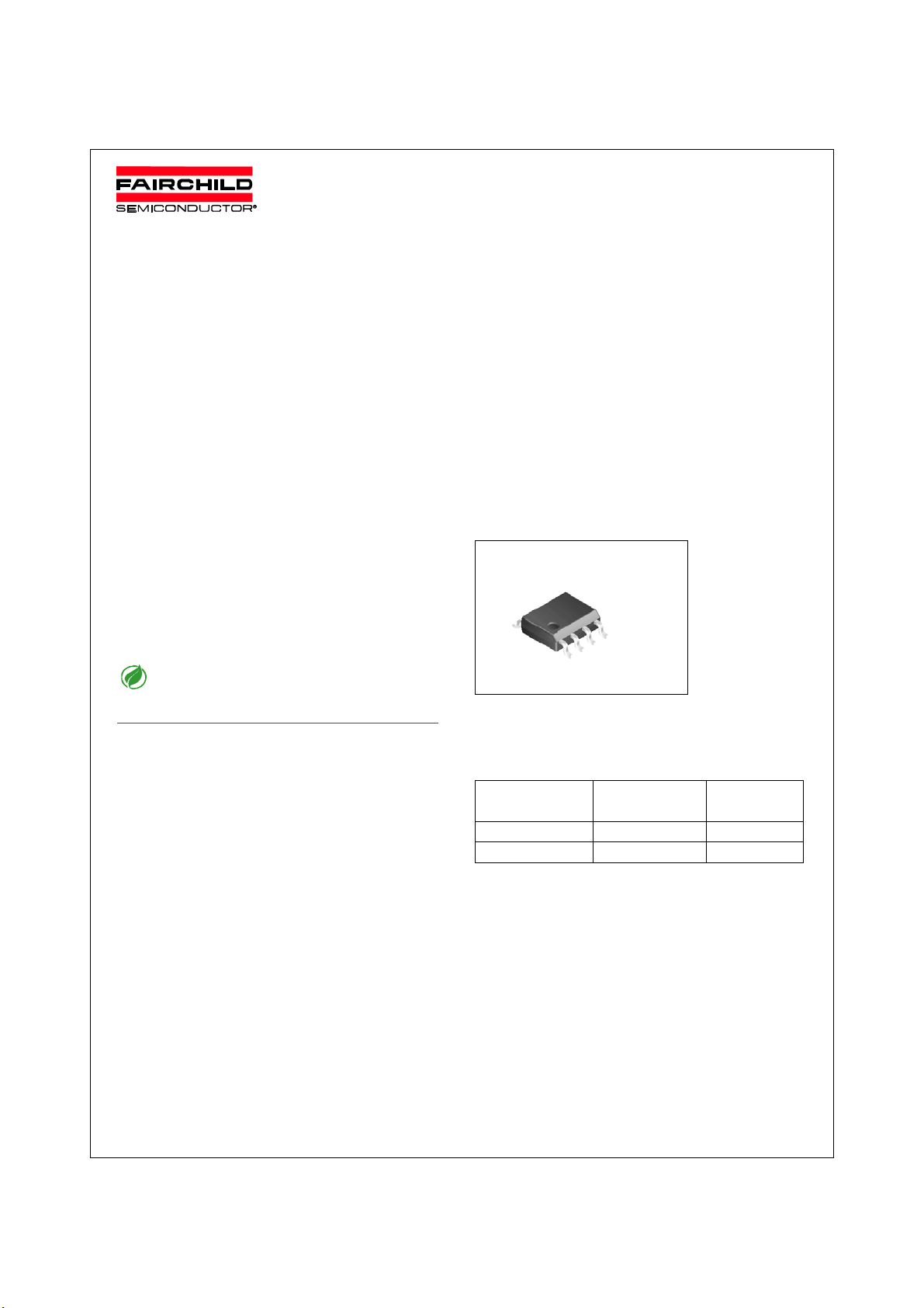
SOIC-8
Ordering Information
Device Package
FAN7085M SOIC-8 -40 °C ~ 125 °C
FAN7085MX SOIC-8 -40 °C ~ 125 °C
X : Tape & Reel type
©2009 Fairchild Semiconductor Corporati on 1 www.fairchildsemi.com
FAN7085_GF085 Rev. 1.0.0
Operating
Temp.

Block Diagrams
VCC
Under Voltage
Reset VCC to GND
Under
Voltage Reset
VB to VS
Pulse Filter
Flip Flop
Brake before
make
FAN7085_GF085 High Side Gate Driver with Recharge FET
VB
HO
VS
RESET-
IN-
GND
Pin Assignments
Pin Definitions
Level Shifter
Logic
Pulse
Filter
1
VCC
2
IN-
3
GND
4
RESET-
VB
HO
NC
VS
ON
Level Shifter
OFF
8
7
6
5
Delay
Recharge Path
Pine Number Pin Name I/O Pin Function Description
1 VCC P Driver supply voltage, typically 5V
2 IN- I Driver control signal input (Negative Logic)
3GNDPGround
4 RESET- I Driver enable input signal (Negative Logic)
5 VS P High side floating offset for MOSFET Source connection
6 NC - No connection (No Bond wire)
7 HO A High side drive output for MOSFET Gate connection
8 VB P Driver output stage supply
FAN7085_GF085 Rev. 1.0.0
2 www.fairchildsemi.com

Absolute Maximum Ratings
Absolute Maximum Ratings indicate sustained limits beyond which damage to the device may occur. All voltage parameters are absolute voltages referenced to GND.
Parameter Symbol Min. Max. Unit
High side floating supply voltage VBS -0.3 25 V
High side driver output stage voltage
Neg. transient: 0.5 ms, external MOSFET off
High side floating supply offset voltage
Neg. transient 0.2 us
High side floating output voltage V
Supply voltage V
Input voltage for IN- V
Input voltage for RESET- V
Power Dissipation
Thermal resistance, junction to ambient
1)
1)
Electrostatic discharge voltage
(Human Body Model)
Charge device model V
Junction Temperature Tj 150 °C
Storage Temperature T
Note: 1) The thermal resistance and power dissipation rating are measu red bellow conditions;
JESD51-2: Integrated Circuit Thermal Test Method Environmental Conditions - Natural condition(StillAir)
JESD51-3: Low Effective Thermal Conductivity Test Board for Leaded Surface Mount Package
VB -5 325 V
Vs -25 300 V
HO VS-0.3 VB+0.3 V
CC -0.3 25 V
IN -0.3 Vcc+0.3 V
RES -0.3 Vcc+0.3 V
Pd 0.625 W
Rthja 200 °C/W
V
ESD
CDM
S
1.5K V
500 V
-55 150 °C
FAN7085_GF085 High Side Gate Driver with Recharge FET
Recommended Operating Conditions
For proper operation the device should be used within the recommended conditions.-40°C <= Ta <= 125°C
Parameter Symbol Min. Max. Unit
High side floating supply voltage(DC)
Transient:-10V@ 0.2 us
High side floating supply offset voltage(DC)
@VBS=7V
High side floating supply offset voltage(Transient)
0.2us @VBS<25V
High side floating output voltage V
Allowable offset voltage Slew Rate
1)
Supply voltage for logic part V
Input voltage for IN- V
Input voltage for RESET- V
Switching frequency
Minimum low input width
Minimum high input width
2)
3)
3)
Minimum operating voltage of VB related to GND V
Ambient temperature T
Note: 1) Guaranteed by design.
2) Duty = 0.5, VBS >=7V
3) Guaranteed by design. Pulse widths below the specified values, may be ignored. Output will either follow the input signal or will ignore it.
No false output state is guaranteed when minimum input width is smaller than tin
4) Guaranteed by design
VB VS+4.5 VS+20 V
S
V
-3 300 V
VS -25 300 V
HO Vs VB V
dv/dt - 50 V/ns
CC 4.5 20 V
IN 0 Vcc V
RESET 0 Vcc V
Fs 200K Hz
tIN(low,min) 1000 - ns
tIN(high,min) 60 - ns
4)
B(MIN)
a -40 125 °C
4- V
FAN7085_GF085 Rev. 1.0.0
3 www.fairchildsemi.com

Statics Electrical Characteristics
Unless otherwise specified, -40°C <= Ta <= 125°C, VCC = 5V, VBS = 7V, VS = 0V, VRESET = 5V, RL = 50Ω, CL = 2.5nF.
Parameter Symbol Conditions Min. Typ. Max. Unit
VCC and VBS Supply Characteristics
V
CC and VBS supply under voltage
positive going threshold
CC and VBS supply under voltage
V
negative going threshold
CC and VBS under voltage hysteresis VCCUVH
V
Under voltage lockout response time tduvcc
Offset supply leakage current I
Quiescent Vcc supply current I
Quiescent VBS supply current I
Quiescent VBS supply current I
VBS drop due to output turn-on
(Design guaranty)
Input Characteristics
High logic level input voltage for IN- V
Low logic level input voltage for IN- V
Low logic level input bias current for IN- I
High logic level input bias current for IN- I
Full up resistance at IN R
High logic level input voltage for RESET- V
Low logic level input voltage for RESET- V
High logic level input current for RESET- I
Low logic level input bias current for RESET- I
Full down resistance at RESET- R
Output characteristics
High level output voltage, V
B - VHO VOH IO=0 - - 0.1 V
Low level output voltage, VHO-GND V
Peak output source current I
Peak output sink current I
Equivalent output resistance R
Recharge Characteristics
Recharge TR turn-on propagation delay T
Recharge TR turn-off propagation delay T
Recharge TR on-state voltage drop V
Dead Time Characteristics
High side turn-off to recharge gate turn-on D
Recharge gate turn-off to high side turn-on D
VCCUV+
Vcc and VBS rising from 0V - 3.7 4.3 V
VBSUV+
VCCUV-
BSUV-
V
Vcc and VBS dropping from 5V 2.8 3.4 - V
- 0.02 0.3 - V
VBSUVH
tduvbs
LK VB=VS=300V - - 200 uA
QCC Vcc=20V - - 500 uA
QBS1 Static mode,
QBS2 Static mode,
ΔV
IN- VIN=0 5 25 60 uA
IN+ VIN=5V - - 5 uA
RES+ VRESET=5V 5 25 60 uA
RES- VRESET=0 5 uA
RES 83 200 1000 ΚΩ
O+ VIN=5V 250 450 - mA
O- VIN=0 250 450 - mA
R
on_rech 47.99.8us
off_rech 0.2 0.4 us
RECH Is=1mA, VIN=5V @125°C 1.2 V
THOFF Vcc=5V, VS=7V 4 7.8 9.8 us
THON Vcc=5V, VS=7V 0.1 0.4 0.7 us
VBS: 6.5V->2.4V or 2.4V->6.5V
BS=7V, VIN=0 or 5V
V
BS=16V, VIN=0 or 5V
V
BS VBS=7V, Cbs=1uF, tdIG-IN =3uS,
IH 0.6VCC --V
IL --0.28VCC V
IN 83 200 1000 ΚΩ
RH 0.6Vcc - - V
RL 0.28Vcc V
OL IO=0 - - 0.1 V
OP 15.5 28 Ω
ON 15.5 28 Ω
TEST=100uS
t
VCC: 6.5V->2.4V or 2.4V->6.5V
0.5
0.5
20
20
us
us
100 uA
200 uA
210 mV
FAN7085_GF085 High Side Gate Driver with Recharge FET
Note: The input parameter are referenced to GND. The VO and IO parameters are referenced to GND.
FAN7085_GF085 Rev. 1.0.0
4 www.fairchildsemi.com

Dynamic Electrical Characteristics
Unless otherwise specified, -40°C <= Ta <= 125°C, VCC = 5V, VBS = 7V, VS = 0V, VRESET = 5V, RL = 50Ω, CL = 2.5nF.
Parameter Symbol Conditions Min. Typ. Max. Unit
Input-to-output turn-on propagation delay tplh 50% input level to 10% output level,
S = 0V
V
Input-to-output turn-off propagation delay t
RESET-to-output turn-off propagation delay t
RESET-to-output turn-on propagation delay t
phl 50% input level to 90% output level
phl_res 50% input level to 90% output level - 0.17 0.5 us
plh_res 50% input level to 10% output level - 0.56 1 us
S = 0V
V
Output rising time tr1 Tj=25°C - 65 200 ns
tr2 - 400 ns
tr3 Tj=25°C,V
tr4 V
BS=16V 65 200 ns
BS=16V - 400 ns
Output falling time tf1 Tj=25°C - 25 200 ns
tf2 - 300 ns
tf3 Tj=25°C,V
tf4 V
BS=16V 25 200 ns
BS=16V - 300 ns
0.56 1 us
- 0.15 0.5 us
FAN7085_GF085 High Side Gate Driver with Recharge FET
FAN7085_GF085 Rev. 1.0.0
5 www.fairchildsemi.com
 Loading...