Fairchild FAN7083_GF085 service manual

FAN7083_GF085
High Side Gate Driver with Reset
FAN7083_GF085 High Side Gate Driver with Reset
November 2009
Features
• Qualified to AEC Q100
• Floating channel designed for bootstrap operation up fully
operational to + 600V
• Tolerance to negative transient voltage on VS pin
• dv/dt immune.
• Gate drive supply range from 10V to 20V
• Under-voltage lockout
• CMOS Schmitt-triggered inputs with pull-down
• High side output in phase with input
• RESET
input is 3.3V and 5V logic compatible
Typical Applications
• Diesel and gasoline injectors/valves
• MOSFET-and IGBT high side driver applications
For Fairchild’s definition of “green” Eco Status, please visit:
http://www.fairchildsemi.com/company/green/rohs_green.html
Description
The FAN7083_GF085 is a high-side gate drive IC with reset
input. It is designed for high voltage and high speed driving of
MOSFET or IGBT, which operates up to 600V. Fairchild's highvoltage process and common-mode noise cancellation technique provide stable operation in the high side driver under
high-dv/dt noise circumstances. An advanced level-shift circuit
allows high-side gate driver operation up to VS=-5V (typical) at
VBS=15V. Logic input is compatible with standard CMOS outputs. The UVLO circuits prevent from malfunction when VCC
and VBS are lower than the specified threshold voltage. It is
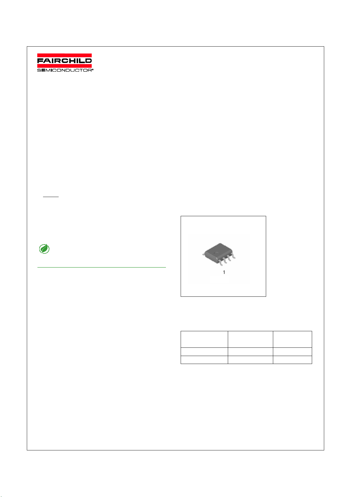
available with space saving SOIC-8 Package. Minimum source
and sink current capability of output driver is 200mA and 400mA
respectively, which is suitable for magnetic-and piezo type injectors and general MOSFET/IGBT based high side driver applications.
SOIC-8
Ordering Information
Device Package
FAN7083M SOIC-8 -40 °C ~ 125 °C
FAN7083MX SOIC-8 -40 °C ~ 125 °C
X : Tape & Reel type
©2009 Fairchild Semiconductor Corporation 1 www.fairchildsemi.com
FAN7083_GF085 Rev. 1.0.0
Operating
Temp.

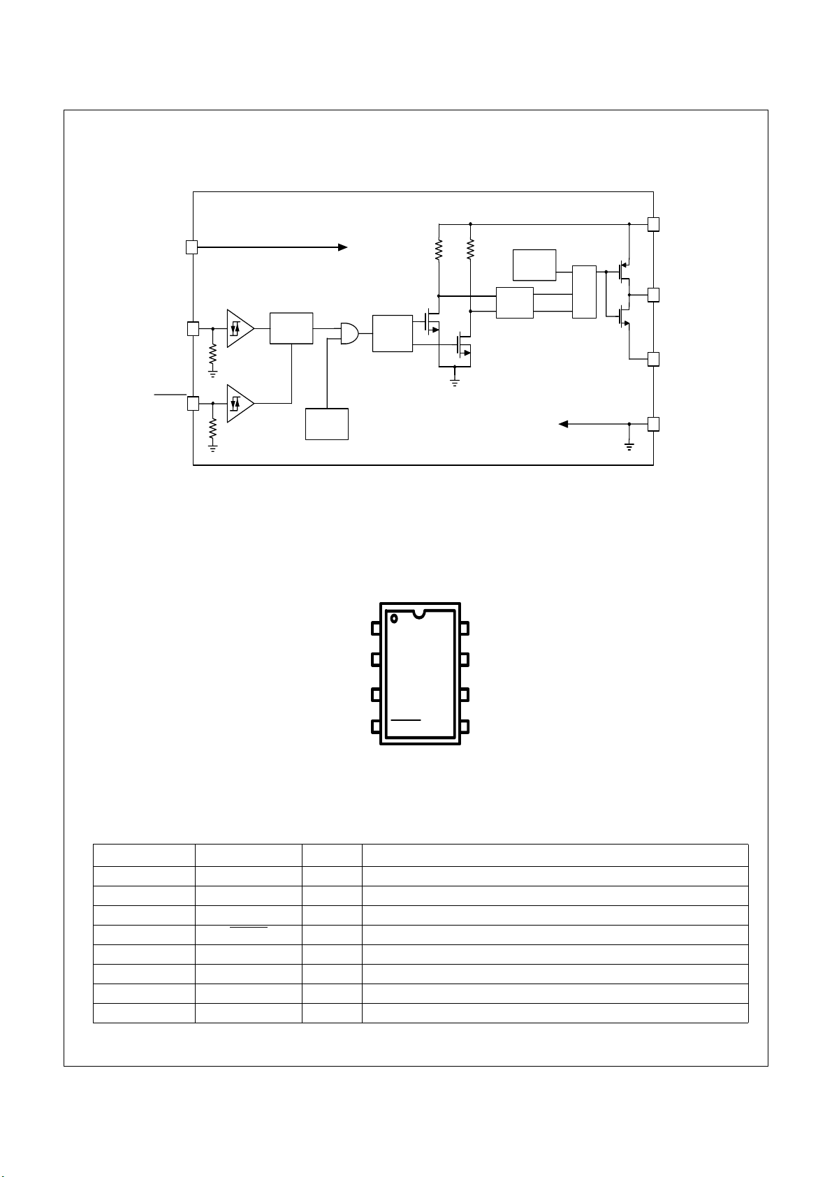
Block Diagrams
VCC
IN
LOGIC
PULSE
GEN
HV Level
Shift
PULSE
FILTER
UV
DETECT
FAN7083_GF085 High Side Gate Driver with Reset
VB
R
Q
R
S
HO
VS
RESET
Pin Assignments
UV
DETECT
1
VCC
2
IN
3
COM
4
RESET
VB
HO
VS
N.C
8
7
6
5
COM
Pin Definitions
Pine Number Pin Name I/O Pin Function Description
1 VCC P Driver supply voltage
2 IN I Logic input for high side gate drive output, in phase with HO
3 COM P Ground
4 RESET
5NC-NC
6 VS P High side floating offset for MOSFET Source connection
7 HO A High side drive output for MOSFET Gate connection
8 VB P Driver output stage supply
FAN7083_GF085 Rev. 1.0.0
I Reset input
2 www.fairchildsemi.com

Absolute Maximum Ratings
Absolute Maximum Ratings indicate sustained limits beyond which damage to the device may occur . All voltage parameters are absolute voltages referenced to COM.
Parameter Symbol Min. Max. Unit
High side floating supply offset voltage VS VB-25 VB+0.3 V
High side floating supply voltage V
High side floating output voltage V
Supply voltage V
Input voltage for IN VIN -0.3 V
Input voltage for RESET
Power Dissipation
Thermal resistance, junction to ambient
1)
1)
Electrostatic discharge voltage
(Human Body Model)
Charge device model V
Junction Temperature Tj 150 °C
Storage Temperature T
Note: 1) The thermal resistance and power dissipation rating are measured bellow conditions;
JESD51-2: Integrated Circuit Thermal Test Method Environmental Conditions - Natural convection(StillAir)
JESD51-3 : Low Effective Thermal Conductivity Test Board for Leaded Surface Mount Package
B -0.3 625 V
HO Vs-0.3 VB+0.3 V
CC -0.3 25 V
cc+0.3 V
VRESET -0.3 Vcc+0.3 V
Pd 0.625 W
Rthja 200 °C/W
V
ESD
CDM
S
1K V
500 V
-55 150 °C
FAN7083_GF085 High Side Gate Driver with Reset
Recommended Operating Conditions
For proper operation the device should be used within the recommended conditions.-40°C <= Ta <= 125°C
Parameter Symbol Min. Max. Unit
High side floating supply voltage
-10V Transient 0.2us
VB Vs + 10
High side floating supply offset voltage(DC) VS -4 (@VBS >= 10V)
-5 (@VBS >= 11.5V)
High side floating supply offset voltage(
Transient)VS -25 (~200ns)
-20(200ns~240ns)
-7(240ns~400ns)
High side floating output voltage V
Allowable offset voltage Slew Rate
1)
Supply voltage V
Input voltage for IN V
Input voltage for RESET
Switching Frequency
2)
Ambient Temperature T
Note : 1) Guaranteed by design.
2) Duty = 0.5
HO Vs VB V
dv/dt - 50 V/ns
CC 10 20 V
IN 0VccV
VRESET 0VccV
Fs 200 KHz
a -40 125 °C
Vs + 20 V
600 V
600 V
FAN7083_GF085 Rev. 1.0.0
3 www.fairchildsemi.com

Statics Electrical Characteristics
Unless otherwise specified, -40°C <= Ta <= 125°C, VCC = 15V, VBS = 15V, VRESET = 5V, VS = 0V, RL = 50Ω, CL = 2.5nF.
Parameter Symbol Conditions Min. Typ. Max. Unit
Vcc and VBS supply Characteristics
CC and VBS supply under voltage
V
positive going threshold
V
CC and VBS supply under voltage
negative going threshold
V
CC and VBS supply under voltage hystere-
sis
VCCUV+
VBSUV+
VCCUVV
BSUV-
VCCUVH
VBSUVH
--9.09.8V
-7.48.4-V
-0.20.6-V
FAN7083_GF085 High Side Gate Driver with Reset
Under voltage lockout response time tduvcc
tduvbs
Offset supply leakage current I
Quiescent V
BS supply current IQBS VIN=0, VRESET=5V - 50 100 uA
Quiescent Vcc supply current I
Quiescent Vcc supply current I
LK VB=VS=600V - - 50 uA
QCC1 VIN=VRESET=0 - 65 140 uA
QCC2 VIN=15V, VRESET=0 - 75 160 uA
VCC: 10V-->7.3V or 7.3V-->10V
VBS: 10V-->7.3V or 7.3V-->10V
Input Characteristics
High logic level input voltage for IN V
Low logic level input voltage for IN V
High logic level input current for IN I
Low logic level input bias current for IN I
High logic level input voltage for RESET
Low logic level input voltage for RESET
High logic level input current for RESET
Low logic level input bias current for RESET
IH - 0.63Vcc - V
IL ---0.4VccV
IN+ VIN=15V - 15 50 uA
IN- VIN=0 - 0 1 uA
VRIH -3.0--V
VRIL ---1.4V
IRIN+ VRESET=5V - 5 30 uA
IRIN- VRESET=0 - 0 1 uA
Output characteristics
High level output voltage, V
Low level output voltage, VO V
Peak output source current I
Peak output sink current I
Equivalent output resistance R
Note: The input parameter are referenced to COM. The VO and IO parameters are referenced to COM.
BIAS- VO VOH IO=0 - - 0.1 V
OL IO=0 - - 0.1 V
O1+ - 200 - - mA
O1- - 400 - - mA
OP 54 75 Ω
ON 24 38 Ω
R
0.5
0.5
2020us
us
FAN7083_GF085 Rev. 1.0.0
4 www.fairchildsemi.com

Dynamic Electrical Characteristics
Unless otherwise specified, -40°C <= Ta <= 125°C, VCC = 15V, VBS = 15V, VRESET = 5V, VS = 0V, RL = 50Ω, CL = 2.5nF.
Parameter Symbol Conditions Min. Typ. Max. Unit
IN-to-output turn-on propagation delay tplh 50% input level to 10% output level,
V
S = 0V
IN-to-output turn-off propagation delay t
RESET-to-output turn-off propagation delay t
RESET-to-output turn-on propagation delay t
Output rising time tr1 Tj=25°C,V
Output falling time tf1 Tj=25°C,V
phl 50% input level to 90% output level
V
S = 0V
phl_res 50% input level to 90% output level - 90 200 ns
plh_res 50% input level to 10% output level - 115 250 ns
BS=15V - 200 400 ns
tr2 - - 500 ns
BS=15V - 25 200 ns
tf2 - - 400 ns
- 115 250 ns
- 90 200 ns
FAN7083_GF085 High Side Gate Driver with Reset
FAN7083_GF085 Rev. 1.0.0
5 www.fairchildsemi.com

Application Information
1. Relationship in input/output and supplies
VCC VBS RESET IN HO
< VCCUVLO- X X X OFF
X < VBSUVLO- X X OFF
XXLOWXOFF
X X X LOW OFF
> VCCUVLO+ > VBSUVLO+ HIGH HIGH ON
Notes:
X menans independent from signal
FAN7083_GF085 High Side Gate Driver with Reset
FAN7083_GF085 Rev. 1.0.0
6 www.fairchildsemi.com
 Loading...