FAN7080_GF085
Half Bridge Gate Driver
FAN7080_GF085 Half Bridge Gate Driver
November 2009
Features
• Qualified to AEC Q100
• Floating channel designed for bootstrap operation fu lly operational to + 600V
• Tolerance to negative transient voltage on VS pin
• VS-pin dv/dt immune.
• Gate drive supply range from 5.5V to 20V
• Under-voltage lockout
• CMOS Schmitt-triggered inputs with pull-down
• High side output in phase with input
• IN input is 3.3V/5V logic compatible and available on 15V
input
• Matched propagation delay for both channels
• Dead time adjustable
Typical Applications
• Junction Box
• Half and full bridge application in the motor drive system
For Fairchild’s definition of “green” Eco Status, please visit:
http://www.fairchildsemi.com/company/green/rohs_green.html
Description
The FAN7080_GF085 is a half-bridge gate drive IC with reset
input and adjustable dead time control. It is designed for high
voltage and high speed driving of MOSFET or IGBT, which
operates up to 600V. Fairchild's high-voltage process and common-mode noise cancellation technique provide stable operation in the high side driver under high-dV/dt noise
circumstances. An advanced level-shift circuit allows high-side
gate driver operation up to VS=-5V (typical) at VBS=15V. Logic
input is compatible with standard CMOS outputs. The UVLO circuits for both channels prevent from malfunction when VCC and
VBS are lower than the specified threshold voltage. Combined
pin function for dead time adjustment and reset shutdown make
this IC packaged with space saving SOIC-8 Package. Minimum
source and sink current capability of output driver is 250mA and
500mA respectively, which is suitable for junction box application and half and full bridge application in the motor drive system.
SOIC-8
Ordering Information
Device Package
FAN7080M SOIC-8 -40 °C ~ 125 °C
FAN7080MX SOIC-8 -40 °C ~ 125 °C
X : Tape & Reel type
©2009 Fairchild Semiconductor Corporati on 1 www.fairchildsemi.com
FAN7080_GF085 Rev. 1.0.0
Operating
Temp.
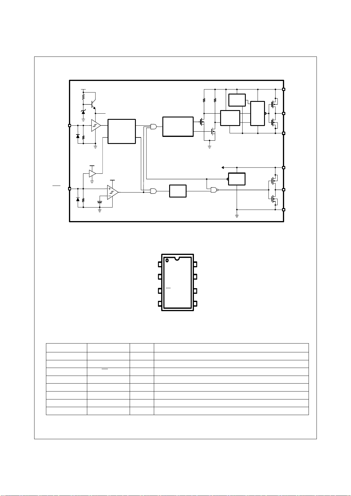
Block Diagrams
FAN7080_GF085 Half Bridge Gate Driver
VCC
IN
500kΩ
vreg
SD/DT
500kΩ
Pin Assignments
vreg
DEADTIME
CONTROL
VCC
PULSE
GENERATOR
DELAY
UVLO
PULSE
FILTER
UVLO
R
RSQ
VB
HO
VS
VCC
LO
COM
1
VCC
2
IN
3
SD/DT
4
COM
VB
HO
VS
LO
8
7
6
5
Pin Definitions
Pine Number Pin Name I/O Pin Function Description
1 VCC P Driver supply voltage
2 IN I Logic input for high and low side gate drive output
3SD
4COMPGround
5 LO A Low side gate drive output for MOSFET Gate connection
6 VS A High side floating offset for MOSFET Source connection
7 HO A High side drive output for MOSFET Gate connection
8 VB P Driver output stage supply
/DT I Shut down input and dead time setting
FAN7080_GF085 Rev. 1.0.0
2 www.fairchildsemi.com
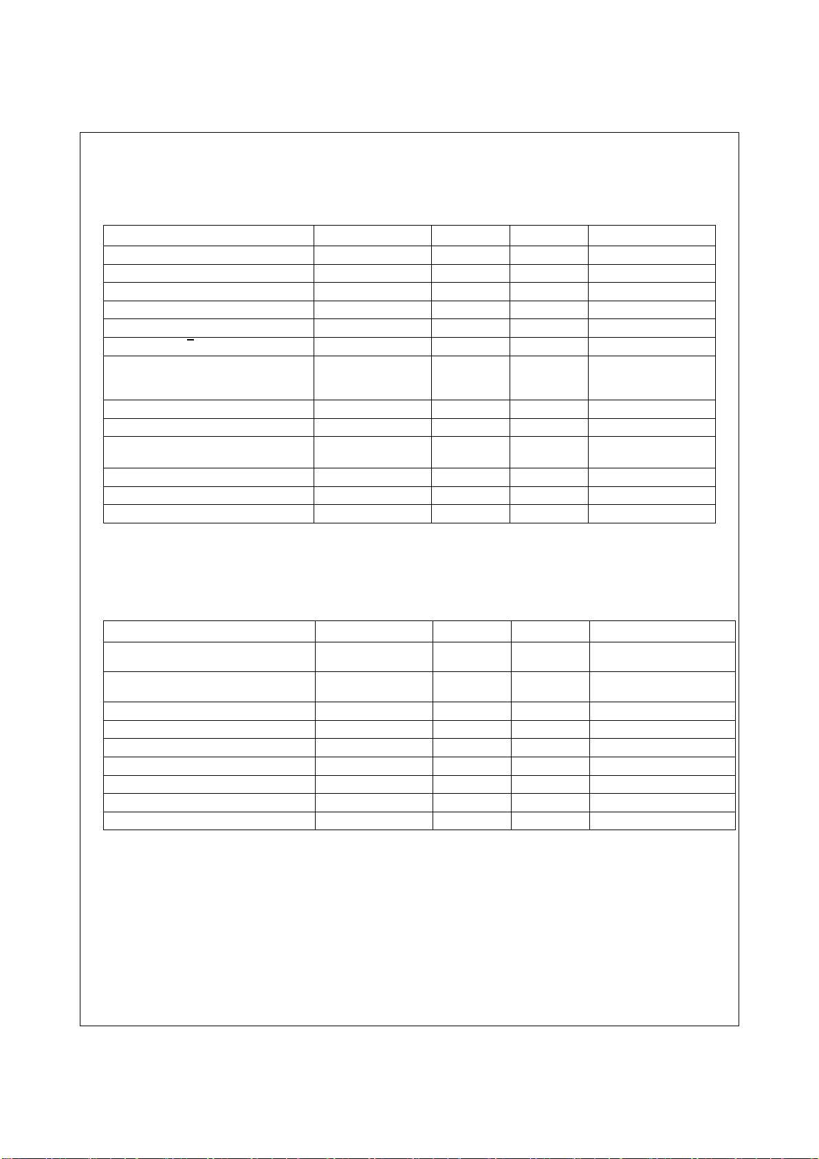
Absolute Maximum Ratings
Absolute Maximum Ratings indicate sustained limits beyond which damage to the device may occur. All voltage parameters are absolute voltages referenced to COM.
Parameter Symbol Min. Max. Unit
High side floating supply offset voltage VS VB-25 VB+0.3 V
High side floating supply voltage V
High side floating output voltage V
Low side output voltage V
Supply voltage V
Input voltage for IN
Input injection current. Full function, no lat ch
up;(Guaranteed by design). Test at 10V and
17V on Eng.Samples
Power Dissipation Pd 0.625 W
Thermal resistance, junction to ambient Rthja 200 °C/W
Electrostatic discharge voltage
(Human Body Model)
Charge device model V
Junction Temperature Tj 150 °C
Storage Temperature T
Note: 1) The thermal resistance and power dissipation rating are measu red bellow conditions;
JESD51-2: Integrated Circuit Thermal Test Method Environmental Conditions - Natural convection(StillAir)
JESD51-3 : Low Effective Thermal Conductivity Test Board for Leaded Surface Mount Package
B -0.3 625 V
HO Vs-0.3 VB+0.3 V
LO -0.3 VCC + 0.3 V
CC -0.3 25 V
VIN -0.3 Vcc+0.3 V
IN -+1 mA
I
V
ESD
CDM
S
1K V
500 V
-55 150 °C
FAN7080_GF085 Half Bridge Gate Driver
Recommended Operating Conditions
For proper operation the device should be used within the recommended conditions.
Parameter Symbol Min. Max. Unit
High side floating supply voltage(DC)
Transient:-10V@ 0.1 us
High side floating supply offset voltage(DC)
Transient: -25V(max) @0.1us @VBS<25V
High side floating output voltage V
Low side output voltage V
Allowable offset voltage Slew Rate
2)
Supply voltage for logic part V
Logic input voltage V
Switching Frequency
3)
Ambient Temperature T
Note: 1) The Vs offset is tested with all supplies biased at 15V differential.
2) Guaranteed by design.
3) When VDT= 1.2V.
1)
VB
VS + 6 VS + 20 V
VS -5 600 V
HO Vs VB V
LO 0VCC V
dv/dt - 50 V/ns
CC 5.5 20 V
IN 0Vcc V
Fs 200 KHz
a -40 125 °C
FAN7080_GF085 Rev. 1.0.0
3 www.fairchildsemi.com
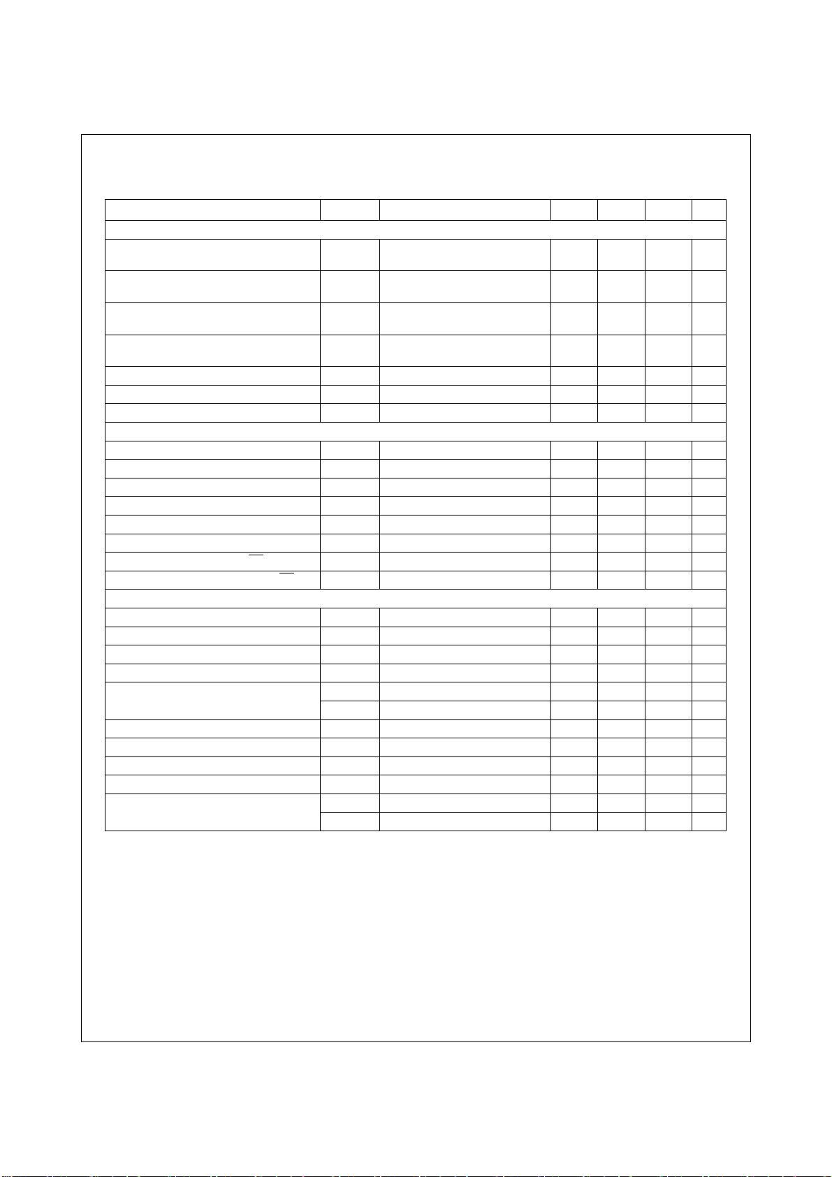
Statics Electrical Characteristics
Unless otherwise specified, -40°C <= Ta <= 125°C, VCC = 15V, VBS = 15V, VS = 0V, CL = 1nF.
Parameter Symbol Conditions Min. Typ. Max. Unit
Vcc and VBS supply Characteristics
V
CC and VBS supply under voltage
positive going threshold
CC and VBS supply under voltage
V
negative going threshold
CC and VBS supply under voltage
V
hysteresis
Under voltage lockout response time tduvcc
Offset supply leakage current I
Quiescent V
BS supply current IQBS VIN=0 OR 5V, VSDT = 1.2V 20 75 150 uA
Quiescent Vcc supply current I
Input Characteristics
High logic level input voltage V
Low logic level input voltage V
High logic level input bias current for IN I
Low logic level input bias current for IN II
VSDT dead time setting range V
VSDT shutdown threshold voltage V
High logic level resistance for SD
/DT RSDT VSDT=5V 100 500 1100 KΩ
Low logic level input bias current for SD
Output characteristics
High level output voltage, V
Low level output voltage, V
CC-VHO VOH(HO) IO=0 - - 0.1 V
HO VOL(HO) IO=0 - - 0.1 V
Output high short circuit pulse current I
Output low short circuit pulse current I
Equivalent output resistance R
High level output voltage, V
Low level output voltage, V
B-VLO VOH(LO) IO=0 - - 0.1 V
LO VOL(LO) IO=0 - - 0.1 V
Output high short circuit pulse current I
Output low short circuit pulse current I
Equivalent output resistance R
VCCUV+
--4.25.5V
VBSUV+
VCCUV-
BSUV-
V
VCCUVH
-2.83.6-V
-0.20.6-V
VBSUVH
VCC: 6V-->2.5V or 2.5V-->6V
tduvbs
LK VB=VS=600V - 20 50 uA
QCC VIN=0 OR 5, VSDT = 1.2V - 350 1000 uA
IH 2.7 - - V
IL --0.8V
IN+ VIN=5V - 10 50 uA
N- VIN=0V - 0 2 uA
DT 1.2 - 5 V
SD -0.81.2V
/DT
ISDT-
O+(HO) 250 300 - mA
O-(HO) 500 600 - mA
OP(HO)
ON(HO) --30Ω
R
O+(LO) 250 - - mA
O-(LO) 500 - - mA
OP(LO) --60Ω
ON(LO) --30Ω
R
VBS: 6V-->2.5V or 2.5V-->6V
VSDT=0V - 1 2 uA
0.5
0.5
-
-
20
20
--60Ω
FAN7080_GF085 Half Bridge Gate Driver
us
us
FAN7080_GF085 Rev. 1.0.0
4 www.fairchildsemi.com
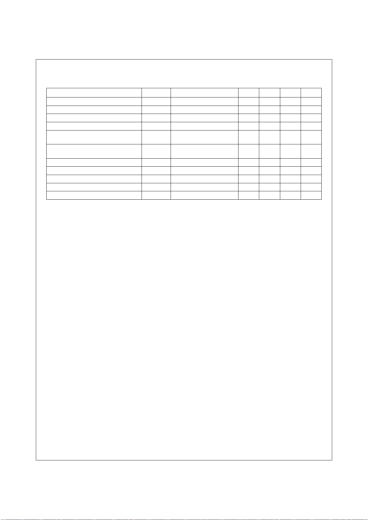
Dynamic Electrical Characteristics
Unless otherwise specified, -40°C <= Ta <= 125°C, VCC = 15V, VBS = 15V, VS = 0V, CL = 1nF.
Parameter Symbol Conditions Min. Typ. Max. Unit
Turn-on propagation delay ton VS=0V - 750 1500 ns
Turn-off propagation delay toff V
Turn -on rising time tr - - 40 150 ns
Turn -off falling time tf - - 25 400 ns
Dead time, LS turn-off to HS turn-on
and HS turn-on to LS turn-off
Dead time matching time MDT DT1 -DT2@ VDT=1.2V
Delay Matching, HS and LS turn-on MTON VDT=1.2V - 25 110 ns
Delay Matching, HS and LS turn-off MTOFF VDT=1.2V 15 60 ns
Shutdown propagation delay Tsd - 180 330 ns
Switching Frequency Fs1 V
DT V
Fs2 V
IN=0 or 5V@ VDT=1.2V
IN=0 or 5V@ VDT=3.3V
V
DT1 -DT2@ VDT=3.3V
S=0V - 130 250 ns
250
1600
CC=VBS=20V - - 200 KHz
CC=VBS=5.5V - - 200 KHZ
650
2100
-35-110
1200
2600
300
FAN7080_GF085 Half Bridge Gate Driver
ns
ns
FAN7080_GF085 Rev. 1.0.0
5 www.fairchildsemi.com
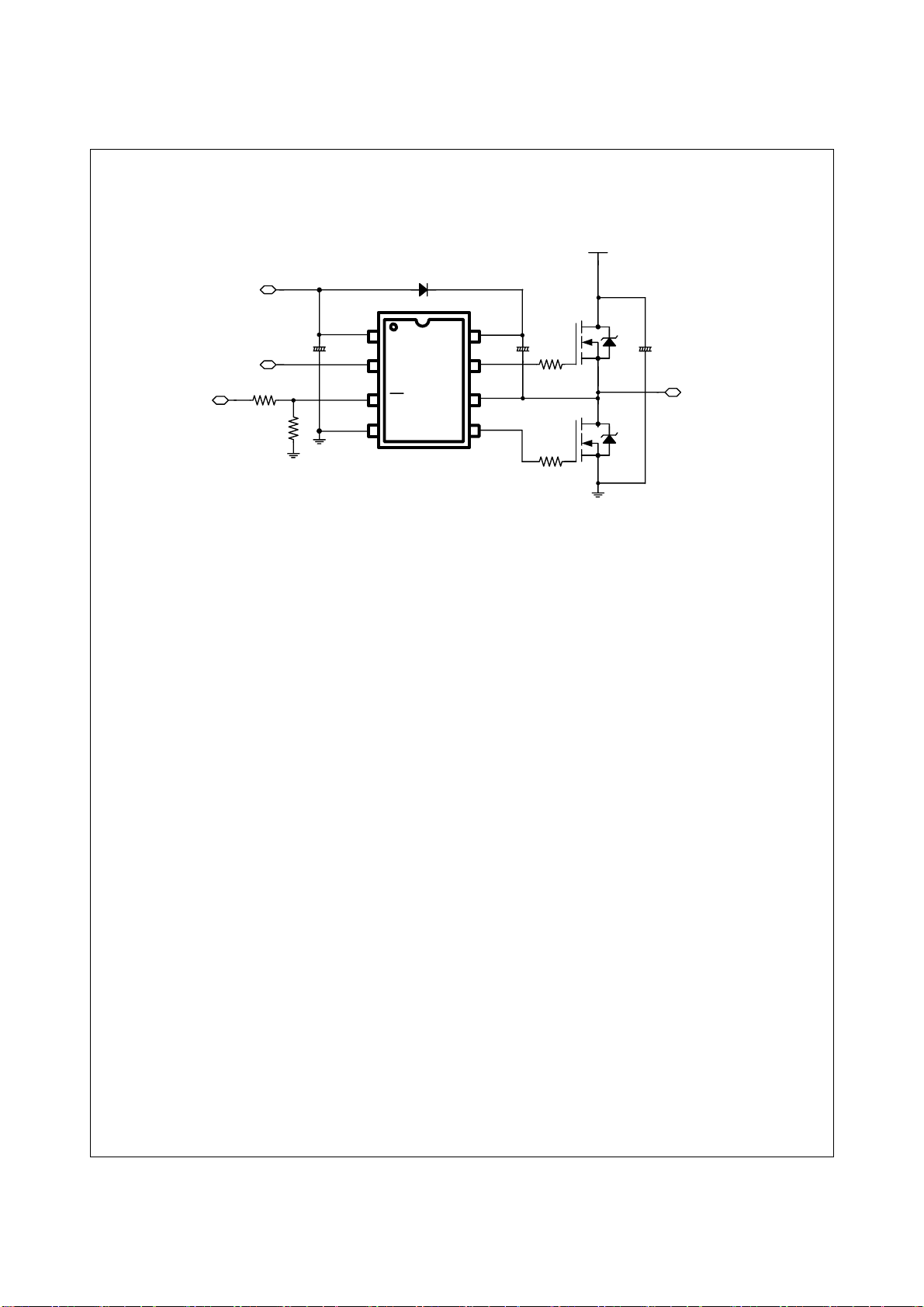
Typical Application Circuit
VCC
FAN7080_GF085 Half Bridge Gate Driver
Up to 600V
1
IN
R1
VDT
SHUTDOWN
/DEAD TIME
R2
VDT = Vdd*R2 / (R1+R2). Vdd is output voltage of Microcontroller.
The operating range that allows a VDT r ange of 1. 2 ~3 .3V.
When pulled lower than V
Care must be taken to avoid bel ow thresh old spi kes on pin 3 that can cause undes ired shut down of the IC.
For this reason the connection of the compon ents bet ween pi n 3 and ground has to be as short as possi ble.
And a capacitor (Typ 0.02uF )between pin3 and COM can prevent this spike. This pin can not be left
floating for the same reason.
DT [Typ. 0.5V] the device is shutdown.
VCC
2
IN
3
SD/DT
4
COM
VB
HO
VS
LO
8
7
To Load
6
5
FAN7080_GF085 Rev. 1.0.0
6 www.fairchildsemi.com
 Loading...