www.fairchildsemi.com
FAN7024
675mW CMOS Mono Power Amplifier with
Shutdown
Features
• Continuous Average Power is 675mW (8Ω)
• Low THD: Typical 0.3% @ Po=500mW
• PSRR@217Hz, Input Terminated : 60dB
• Do Not Need Output Coupling Capacitor or Bootstrap
Capacitor
• Low Shutdown Current: Typical 0.1µA
• Shutdown: High Active
• Click & Pop Suppression circuitry
• Built in TSD Circuit
Typical Applications
• Cellular Phone
•PDA
• Portable Audio Systems
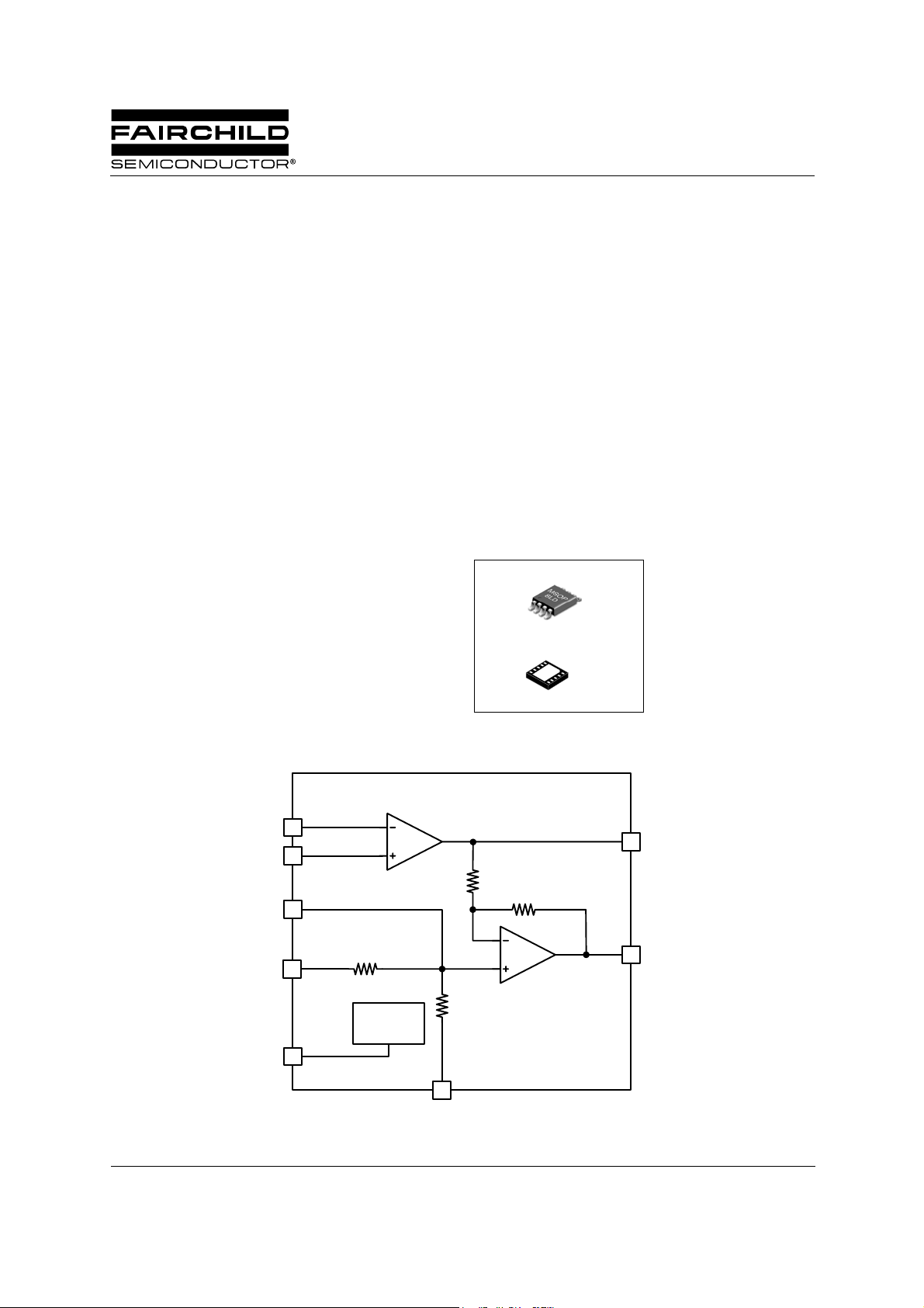
Internal Block Diagram
Description
The FAN7024 is a bridge connected audio power amplifier
capable of delivering 675mW of continuous average power
to an 8Ω load with less than 0.3%(THD) from a 5V power
supply. The FAN7024 requires few external components and
operates on low supply voltage from 2.3V to 5.5V. Since the
FAN7024 does not require output coupling capacitors,
bootstrap capacitors, or snubber networks, it is ideally suited
for low power portable systems that require minimum
volume and weight. The FAN7024 features an externally
controlled gain and low power consumption shutdown mode
(0.1uA,typ.). Additional FAN7024 features include thermal
shutdown protection, unity gain stability, and external gain
set.
8MSOP
1
10MLP
1
BOTTOM VIEW
IN-
4
3
IN+
2
BP
6
VDD
1
SD
©2003 Fairchild Semiconductor Corporation
100KΩ
Shutdown
BIAS
&
20KΩ
7
VDD/2
100KΩ
GND
VO1
5
20KΩ
8
VO2
Rev. 1.0.0

FAN7024
Pin Assignments
GND
8 7 6 5
O1VDDVO2
V
V
V
NC
DD
NC
O1
10
9
8
7
6
10MLP
(BOTTOM VIEW)
0 2 4
YWW
1 2 3 4
SD BP IN-
IN+
8MSOP
Pin Definitions
Pin Number Pin Name Pin Function Description
1(1) SD Shutdown. Hold high to shutdown, hold low for normal operation
2(2) BP Bypass. Tap to voltage divider for internal mid-supply bias
3(4) IN+ Noninverting input
4(5) IN- Inverting input
5(6) V
6(8) V
O1
DD
7(3) GND Ground connection for circuitry
8(10) V
O2
Power amplifier output1
Supply voltage input
Power amplifier output2
1
SDVO2
2
BP
3
GND
4
IN+
5
IN-
( ) : 10MLP
2
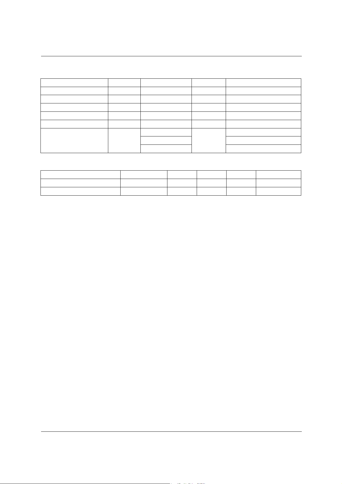
Absolute Maximum Ratings (Note 2)
Parameter Symbol Value Unit Remark
Maximum Supply Voltage V
Input Voltage V
Power Dissipation P
Storage Temperature T
Junction Temperature T
Thermal Resistance
Junction to Ambient
Rthja
DD
IN
D
STG
J
Internally Limited W
6.0 V
-0.3 ~ VDD+0.3 V
-65 ~ +150 °C
150 °C
190
166 10MLP, Single-Layer
°C/W
8MSOP
50 10MLP, Multi-Layer
Recommended Operating Conditions (Note 2)
Parameter Symbol Min. Typ. Max. Unit
Operating Supply Voltage V
Operating Temperature T
DD
OPR
2.3 - 5.5 V
-40 - 85 °C
FAN7024
3
FAN7024
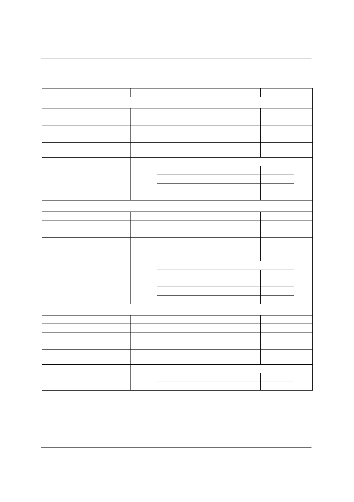
Electrical Characteristics(Note1,2)
(R
= 8Ω, Ta = 25°C, unless otherwise specified)
L
Parameter Symbol Conditions Min. Typ. Max. Unit
VDD = 5.0V, UNLESS OTHERWISE SPECIFIED
Quiescent Power Supply Current I
Shutdown Current I
Output Offset Voltage V
DD
SD
OS
Output Power P
Total Harmonic Distortion+Noise THD+N
Power Supply Rejection Ratio PSRR
VDD = 3.3V, UNLESS OTHERWISE SPECIFIED
Quiescent Power Supply Current I
Shutdown Current I
Output Offset Voltage V
DD
SD
OS
Output Power P
Total Harmonic Distortion+Noise THD+N
Power Supply Rejection Ratio PSRR
V
= 0V,IO = 0A - 2.3 5.5 mA
IN
V
= V
SD
DD
V
= 0V - 0 50 mV
IN
THD = 1%(Max.), f = 1kHz - 675 - mW
O
= 500mW
P
O
, Av=6dB,
rms
20Hz<f<20kHz, BW<80kHz
V
=200mV
ripple
sinp-p
-0.11.0µA
-
0.2
f=217Hz(Terminated input) - 63 -
f=1kHz(Terminated input) - 65 -
f=217Hz(Unterminated input) - 70 -
f=1kHz(Unterminated input) - 70 -
V
= 0V,IO = 0A - 1.9 4 mA
IN
V
= V
SD
DD
V
= 0V - 0 50 mV
IN
THD = 1%(Max.), f = 1kHz - 265 - mW
O
PO = 250mW
, Av=6dB,
rms
20Hz<f<20kHz, BW<80kHz
V
=200mV
ripple
sinp-p
-0.11.0µA
-
0.3
f=217Hz(Terminated input) - 63 -
f=1kHz(Terminated input) - 65 -
f=217Hz(Unterminated input) - 70 -
f=1kHz(Unterminated input) - 70 -
-
-
%
dB
%
dB
VDD = 2.6V, UNLESS OTHERWISE SPECIFIED
Quiescent Power Supply Current I
Shutdown Current I
Output Offset Voltage V
DD
SD
OS
Output Power P
Total Harmonic Distortion+Noise THD+N
Power Supply Rejection Ratio PSRR
V
= 0V,IO = 0A - 1.7 3.5 mA
IN
V
= V
SD
DD
V
= 0V - 0 50 mV
IN
THD = 1%(Max.), f = 1kHz - 130 - mW
O
PO = 100mW
, Av=6dB,
rms
20Hz<f<20kHz, BW<80kHz
V
=200mV
ripple
sinp-p
-0.11.0µA
-
0.4
%
dBf=217Hz(Terminated input) - 63 -
f=1kHz(Terminated input) - 65 -
Note 1 : All voltages are measured with respect to the ground pin, unless otherwise specified.
Note 2 : Absolute Maximum Ratings indicate limits beyond which damage to the device may occur. Recommended Operating
Conditions indicate conditions for which the device is functional, but do not guarantee specific performance limits. Electrical
Characteristics state DC and AC electrical specifications under particular test conditions which guarantee specific
performance limits. This assumes that the device is whitin the Operating Ratings. Specifications are not guaranteed for
parameters where no limit is given, however, the typical value is a good indication of device performance.
4
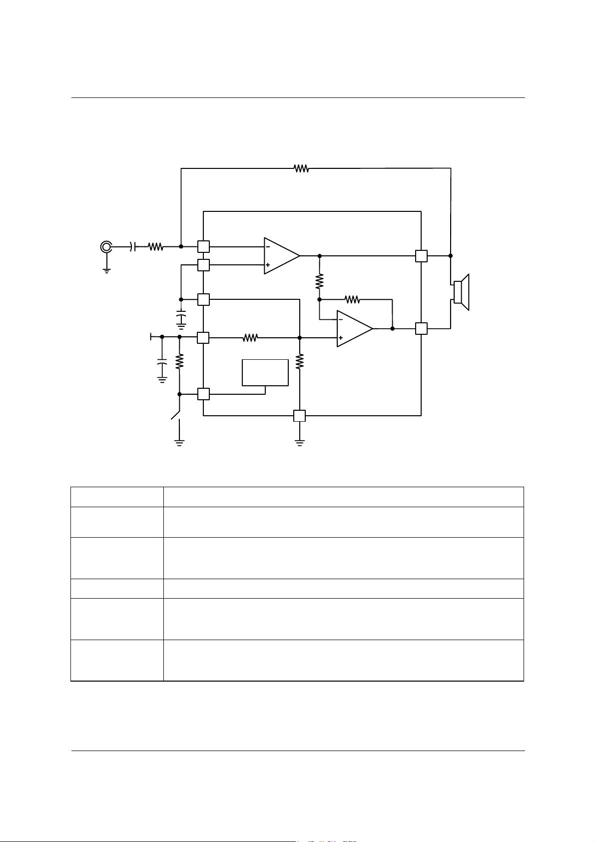
Typical Application Circuit
R
20KΩ
FAN7024
F
C
0.39uF
R
I
I
20KΩ
1uF
C
B
V
DD
C
S
10uF
20KΩ
NC
IN-
4
3
IN+
20KΩ
2
BP
100KΩ
6
VDD
BIAS
&
Shutdown
1
SD
7
VDD/2
100KΩ
GND
20KΩ
External Components Descriptions
Components Functional Descriptions
1. R
I
The inverting input resistor which sets the closed-loop gain in conjunction with Rf. This
resistor also forms a high pass filter with C
at fc=1/(2πRICI)
I
VO1
VO2
5
R
L
8Ω/16Ω/32Ω
8
2. C
3. R
4. C
5. C
The input coupling capacitor blocks the DC voltage at the amplifier’s input terminals. Also
I
F
creates a high pass with RI at fc=1/(2πRICI). Refer to the section, Proper Selection of
External Components, for an explanation of how to determine the value of C
.
I
The feedback resistor which sets closed-loop gain in conjunction with RI.
The supply bypass capacitor which provides power supply filtering. Refer to the
S
Application Information section for proper placement and selection of the supply
bypass capacitor.
The bypass pin capacitor which provides half-supply filtering. Refer to the Proper
B
Selection of External Components section for information concerning proper placement
and selecting CB’s value.
5
FAN7024
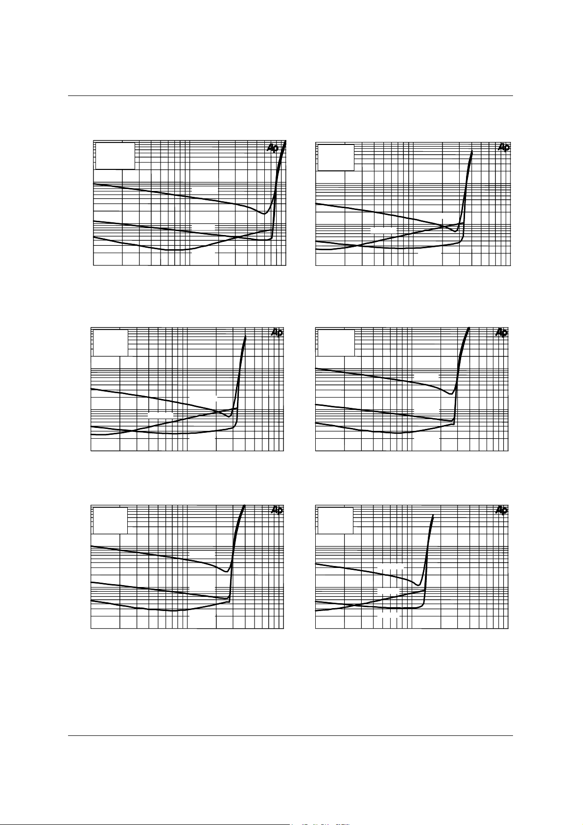
Performance Chracteristics
10
10
VDD=5V
VDD=5V
R
R
=8Ω
=8Ω
L
L
Av=6dB
Av=6dB
BW < 80kHz
BW < 80kHz
1
1
THD + N (%)
THD + N (%)
0.1
0.1
0.01
0.01
10m 100m
10m 100m
50m 500m
50m 500m
Figure 1. THD+N vs. Output Power Figure 2. THD+N vs. Output Power
10
10
VDD=5V
VDD=5V
R
R
=32Ω
=32Ω
L
L
Av=6dB
Av=6dB
BW < 80kHz
BW < 80kHz
1
1
f = 20KHz
f = 20KHz
f = 1KHz
f = 1KHz
f = 20Hz
f = 20Hz
Output Power (W)
Output Power (W)
10
10
VDD=5V
VDD=5V
=16Ω
=16Ω
R
R
L
L
Av=6dB
Av=6dB
BW < 80kHz
BW < 80kHz
1
1
f = 20KHz
100m 1500m50m
100m 1500m50m
f = 20KHz
f = 1KHz
f = 1KHz
f = 20KHz
f = 20KHz
THD + N (%)
THD + N (%)
0.1
0.1
0.01
0.01
1
1
10m
10m
10
10
VDD=3.3V
VDD=3.3V
R
R
=8Ω
=8Ω
L
L
Av=6dB
Av=6dB
BW < 80kHz
BW < 80kHz
1
1
f = 20Hz
f = 20Hz
Output Power (W)
Output Power (W)
THD + N (%)
THD + N (%)
THD + N (%)
THD + N (%)
0.1
0.1
0.01
0.01
0.1
0.1
0.01
0.01
10m
10m
10
10
1
1
10m
10m
f = 20KHz
f = 20KHz
f = 20Hz
f = 20Hz
f = 1KHz
f = 1KHz
100m 1500m50m
100m 1500m50m
Output Power (W)
Output Power (W)
Figure 3. THD+N vs. Output Power
VDD=3.3V
VDD=3.3V
R
R
=16Ω
=16Ω
L
L
Av=6dB
Av=6dB
BW < 80kHz
BW < 80kHz
f = 20KHz
f = 20KHz
f = 1KHz
f = 1KHz
f = 20Hz
f = 20Hz
100m 1500m50m
100m 1500m50m
Output Power (W)
Output Power (W)
Figure 5. THD+N vs. Output Power
THD + N (%)
THD + N (%)
THD + N (%)
THD + N (%)
0.1
0.1
0.01
0.01
0.1
0.1
0.01
0.01
10m
10m
10
10
1
1
10m
10m
f = 1KHz
f = 1KHz
f = 20Hz
f = 20Hz
100m 1500m50m
100m 1500m50m
Output Power (W)
Output Power (W)
Figure 4. THD+N vs. Output Power
VDD=3.3V
VDD=3.3V
R
R
=32Ω
=32Ω
L
L
Av=6dB
Av=6dB
BW < 80kHz
BW < 80kHz
f = 20KHz
f = 20KHz
f = 20Hz
f = 20Hz
f = 1KHz
f = 1KHz
100m 1500m50m
100m 1500m50m
Output Power (W)
Output Power (W)
Figure 6. THD+N vs. Output Power
6
 Loading...