www.fairchildsemi.com
FAN7005
200mW Stereo Power Amplifier with Shutdown
Features
• 200mW and 300mW Power Per Each Channel into 8Ω
Load with Less Than 0.3% and 10% THD+N,
Respectively
• Low Shutdown Current : 0.1µA(Typ.)
• No Bootstrap Capacitors or Snubber Circuits are
Necessary
• Stable Unity-Gain
• Guaranteed Stability Under No Load Condition
• External Gain Configuration Capability
• Thermal Shutdown Protection Circuitry
• Pop Reduction Circuit
• 8MSOP Surface Mount Packaging
Typical Applications
•PDA
•MP3/CDP
• Portable Audio System
Description
The FAN7005 is a dual, fully differential audio power amplifier delivering 200mW(typ.) of continuous power into an 8Ω
load. When driving 200mW into an 8Ω load from a 5V
power supply, the FAN7005 has less than 0.3% of THD+N
over the entire audible frequency range. To reduce the power
consumption in portable applications, the FAN7005 provides
a shutdown capability. In shutdown condition, current consumption is reduced to less than 2µA. The FAN7005 is
designed specifically to provide high quality output power
with a minimal amount of external components using surface
mount packaging. Since the additional snubber circuits or
bootstrap capacitors are not needed, the FAN7005 is well
suited for portable systems and other hand-held devices.
8MSOP
1
8SOP
1
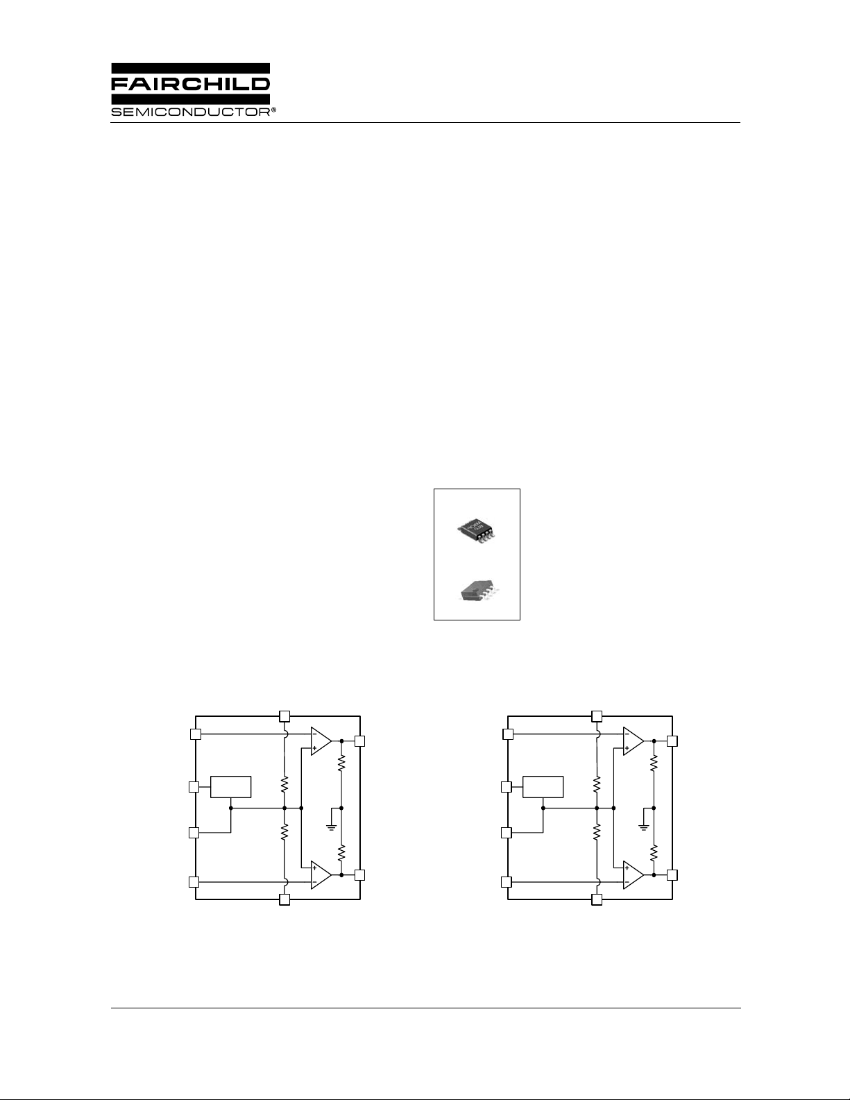
Internal Block Diagram
VDD
6
8
RIN
SDH
3
1
BP
LIN
4
©2002 Fairchild Semiconductor Corporation
100kΩ
Bias
VDD/2
100kΩ
2
GND
FAN7005MU(8MSOP)
20kΩ
20kΩ
7
5
ROUT
LOUT
RIN
SDH
BP
LIN
2
5
Bias
3
6
FAN7005M(8SOP)
100kΩ
VDD/2
100kΩ
VDD
8
4
GND
20kΩ
20kΩ
1
ROUT
7
LOUT
Rev. 1.0.0
FAN7005
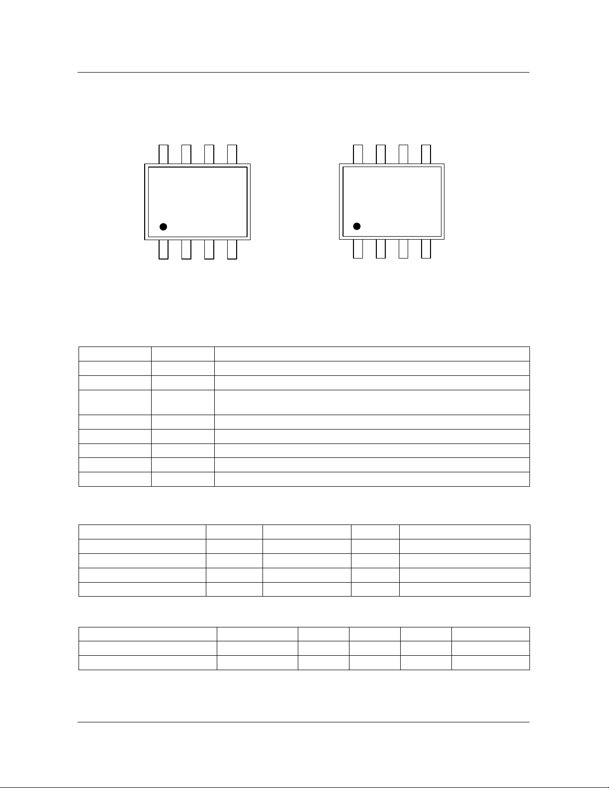
Pin Assignments
8 7 6 5
ROUT
LINLOUTVDD
LOUTVDDRIN
8 7 6 5
SDH
0 0 5
F
YWW
1 2 3 4
BP GND LIN
FAN7005MU(8MSOP) FAN7005M(8SOP)
SDH
1 2 3 4
ROUT
YWW
7 0 0 5
RIN
Pin Definitions
Pin Number Pin Name Pin Function Description
1(3) BP Tap to Voltage Divider for Internal a Half Supply Bias
2(4) GND Ground Connection for Circuitry
3(5) SDH
4(6) LIN Signal Input Left-Channel
5(7) LOUT Output Left-Channel
6(8) VDD Supply Voltage Input
7(1) ROUT Output Right-Channel
8(2) RIN Signal Input Right-Channel
Shutdown all Amplifier, Hold High to Shutdown, Hold Low for Normal
Operation
BP GND
Y ; Yearly Code
WW ; Weekly Code
( ) : 8SOP
Absolute Maximum Ratings
Parameter Symbol Value Unit Remark
Maximum Supply Voltage V
Storage Temperature T
Power Dissipation (Note3) P
Thermal Resistance (Note3) Rthja 210 °C/W 8MSOP, Junction to Ambient
DD
STG
D
(Note2)
6.0 V -
-65 ~ +150 °C-
Internally Limited W -
Operating Ratings
Parameter Symbol Min. Typ. Max. Unit
Operating Supply Voltage V
Operating Temperature T
2
DD
OPR
2.7 - 5.5 V
-40 - +85 °C
FAN7005
Electrical Characteristics (Notes1,2)
(Ta = 2 5 °C, unless otherwise specified)
Parameter Symbol Conditions Min. Typ. Max. Unit
VDD = 5.0V, UNLESS OTHERWISE SPECIFIED
Quiescent Power Supply Current I
Shutdown Current I
Output Offset Voltage V
Output Power P
Total Harmonic Distortion+Noise THD+N
Power Supply Rejection Ratio PSRR CB=1µF, V
VDD = 3.0V, UNLESS OTHERWISE SPECIFIED
Quiescent Power Supply Current I
Shutdown Current I
Output Offset Voltage V
Output Power P
Total Harmonic Distortion+Noise THD+N
Power Supply Rejection Ratio PSRR CB=1µF, V
No Input, No Load - 2.2 5.0 mA
DD
VSD=V
SD
OFFVIN
THD=0.3% (Max.),
f=1kHz
O
THD=10% (Max.),
f=1kHz
DD
=0V -25 0 25 mV
R
=8Ω 125 200 - mW
L
RL=32Ω -85-mW
=8Ω - 300 - mW
R
L
R
=32Ω -110-mW
L
-0.12.0µA
RL=8Ω, Po=125mWrms, f=1kHz - 0.04 - %
RL=32Ω, Po=75mWrms, f=1kHz - 0.015 - %
=250mVrms, f=1kHz - 50 - dB
RIPPLE
No Input, No Load - 1.8 - mA
DD
VSD=V
SD
OFFVIN
THD=0.3% (Max.),
f=1kHz
O
THD=10% (Max.),
f=1kHz,
DD
=0V -25 0 25 mV
RL=8Ω -70-mW
RL=32Ω -30-mW
RL=8Ω -95-mW
RL=32Ω -35-mW
--2.0µA
RL=8Ω, Po=70mWrms, f=1kHz - 0.05 - %
RL=32Ω, Po=25mWrms, f=1kHz - 0.02 - %
=200mVrms, f=1kHz - 50 - dB
RIPPLE
Note:
1. All voltages are measured with respect to the ground pin, unless otherwise specified.
2. Absolute Maximum Ratings indicate limits beyond which damage to the device may occur. Operating Ratings indicate
conditions for which the device is functional, but do not guarantee specific performance limits. Electrical Characteristics state
DC and AC electrical specifications under particular test conditions which guarantee specific performance limits. This
assumes that the device is within the Operating Ratings. Specifications are not guaranteed for parameters where no limit is
given, however, the typical value is a good indication of device performance.
3. The maximum power dissipation must be derated at elevated temperatures and is dictated by T
temperature T
150°C, and the typical junction-to-ambient thermal resistance, when board mounted, is 210°C/W for the 8MSOP Package.
. The maximum allowable power dissipation is P
A
DMAX
= (T
JMAX -TA
)/Rthja. For the FAN7005, T
, Rthja and the ambient
JMAX
JMAX
=
3
FAN7005
Performance Characteristics
Table of Graphs
Figure
THD+N, Total Harmonic Distortion plus Noise
Power Dissipation 24,25
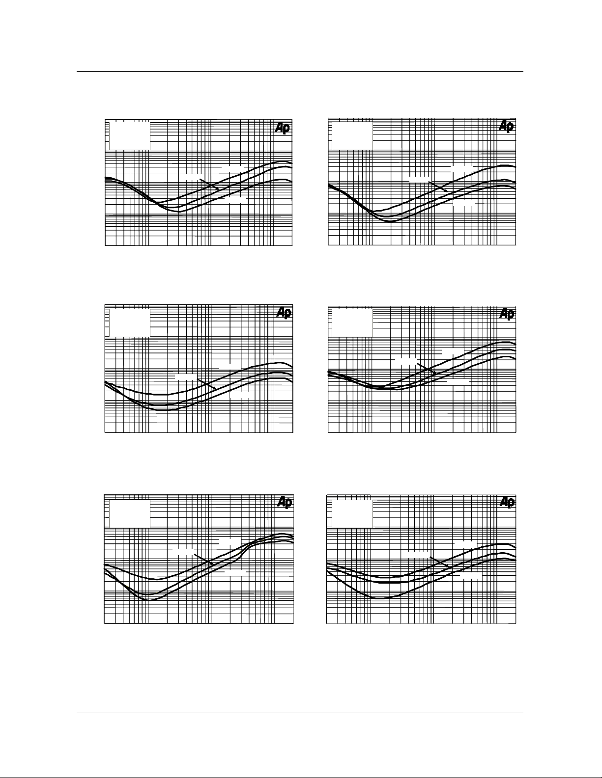
THD+N, Total Harmonic Distortion plus Noise
PSRR, Power Supply Rejection Ratio 13,14
Cross Talk 15
Output Level 16,17,18,19,20
Noise Floor 21
Supply Current
Output Power 26,27
Dropout Voltage 30
Supply Current Shutdown Voltage 23
Output Power Load Resistance 28,29
Power Dissipation Ambient Temperature 31
Output Power
Frequency
Supply Voltage
1,2,3,4,5,6
7,8,9,10,11,12
22
4
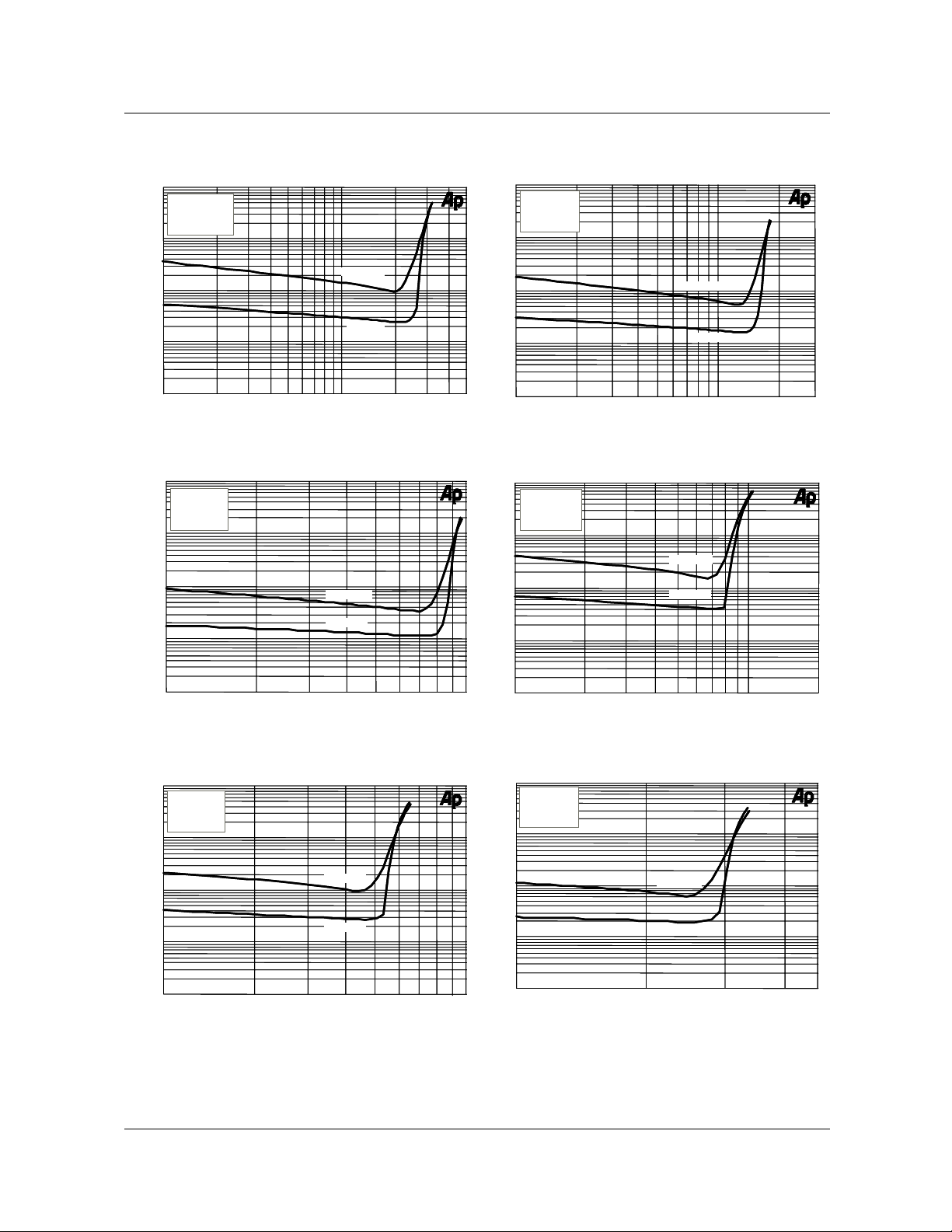
Typical Performance Characteristics
10
10
VDD=5V
VDD=5V
RL=8Ω
RL=8Ω
Av=-1
Av=-1
BW < 80kHz
BW < 80kHz
1
1
f = 20kHz
f = 20kHz
0.1
0.1
THD + N (%)
THD + N (%)
f = 1kHz
0.01
0.01
0.001
0.001
THD + N (%)
THD + N (%)
0.01
0.01
10m
10m
10
10
1
1
0.1
0.1
Outpu t Powe r (W)
Outpu t Powe r (W)
Figure 1. THD+N vs. Output Power Figure 2. THD+N vs. Output Power
VDD=5V
VDD=5V
RL=32Ω
RL=32Ω
Av=-1
Av=-1
BW < 80kHz
BW < 80kHz
f = 1kHz
0.1
0.1
f = 20kHz
f = 20kHz
f = 1kHz
f = 1kHz
0.5
0.5
THD + N (%)
THD + N (%)
0.01
0.01
0.001
0.001
THD + N (%)
THD + N (%)
0.01
0.01
10
10
1
1
0.1
0.1
10m
10m
10
10
1
1
0.1
0.1
VDD=5V
VDD=5V
RL=16Ω
RL=16Ω
Av=-1
Av=-1
BW < 80kHz
BW < 80kHz
VDD=3V
VDD=3V
RL=8Ω
RL=8Ω
Av=-1
Av=-1
BW < 80kHz
BW < 80kHz
f = 20kHz
f = 20kHz
f = 1kHz
f = 1kHz
Output Power (W )
Output Power (W )
f = 20kHz
f = 20kHz
f = 1kHz
f = 1kHz
FAN7005
0.1 0.3
0.1 0.3
0.001
0.001
10m
10m
Output Power (W )
Output Power (W )
50m 0.1
50m 0.1
Figure 3. THD+N vs. Output Power Figure 4. THD+N vs. Output Power
10
10
VDD=3V
VDD=3V
RL=16Ω
RL=16Ω
Av=-1
Av=-1
BW < 80kHz
BW < 80kHz
1
1
0.1
0.1
THD + N (%)
THD + N (%)
0.01
0.01
0.001
0.001
10m 50m 0.1
10m 50m 0.1
Output Power (W)
Output Power (W)
f = 20kHz
f = 20kHz
f = 1kHz
f = 1kHz
Figure 5. THD+N vs. Output Power Figure 6. THD+N vs. Output Power
0.001
0.001
0.1
0.1
THD + N (%)
THD + N (%)
0.01
0.01
0.001
0.001
10m
10m
10
10
1
1
10m
10m
VDD=3V
VDD=3V
RL=32Ω
RL=32Ω
Av=-1
Av=-1
BW < 80kHz
BW < 80kHz
0.1 0.2
Output Power (W)
Output Power (W)
f = 20kHz
f = 20kHz
f = 1kHz
f = 1kHz
20m 30m 40m 50m
20m 30m 40m 50m
Output P ower (W )
Output P ower (W )
0.1 0.2
5
FAN7005
Typical Performance Characteristics (Continued)
10
10
VDD=5V
VDD=5V
RL=8Ω
RL=8Ω
Po=200mW
Po=200mW
BW < 80kHz
BW < 80kHz
1
1
Av = -5
Av = -2
0.1
0.1
THD + N (%)
THD + N (%)
0.01
0.01
0.001
0.001
20 20k50 100 200 500 1k 2k 5k 10k
20 20k50 100 200 500 1k 2k 5k 10k
Av = -2
Frequency (Hz)
Frequency (Hz)
Av = -5
Av = -1
Av = -1
Figure 7. THD+N vs. Frequency Figure 8. THD+N vs. Frequency
10
10
VDD=5V
VDD=5V
RL=32Ω
RL=32Ω
Po=70mW
Po=70mW
BW < 80kHz
BW < 80kHz
1
1
Av = -5
Av = -5
Av = -1
Av = -1
THD + N (%)
THD + N (%)
0.01
0.01
0.1
0.1
Av = -2
Av = -2
10
10
1
1
0.1
0.1
THD + N (%)
THD + N (%)
0.01
0.01
0.001
0.001
20 20k50 100 200 500 1k 2k 5k 10k
20 20k50 100 200 500 1k 2k 5k 10k
10
10
1
1
0.1
0.1
THD + N (%)
THD + N (%)
0.01
0.01
VDD=5V
VDD=5V
RL=16Ω
RL=16Ω
Po=120mW
Po=120mW
BW < 80kHz
BW < 80kHz
VDD=3V
VDD=3V
RL=8Ω
RL=8Ω
Po=70mW
Po=70mW
BW < 80kHz
BW < 80kHz
Av = -2
Av = -2
Frequency (Hz)
Frequency (Hz)
Av = -2
Av = -2
Av = -5
Av = -5
Av = -5
Av = -5
Av = -1
Av = -1
Av = -1
Av = -1
0.001
0.001
0.1
0.1
THD + Naaaa (%)
THD + Naaaa (%)
0.01
0.01
0.001
0.001
10
10
1
1
20
20
0.001
0.001
20
THD + N (%)
THD + N (%)
0.01
0.01
0.001
0.001
0.1
0.1
10
10
1
1
20
Frequency (Hz)
Frequency (Hz)
Figure 10. THD+N vs. Frequency
VDD=3V
VDD=3V
RL=32Ω
RL=32Ω
Po=20mW
Po=20mW
BW < 80kHz
BW < 80kHz
Av = -2
Av = -2
20
20
Frequency (Hz)
Frequency (Hz)
Frequency (Hz)
Frequency (Hz)
Figure 9. THD+N vs. Frequency
VDD=3V
VDD=3V
RL=16Ω
RL=16Ω
Po=50mW
Po=50mW
BW < 80kHz
BW < 80kHz
Av = -2
Av = -2
Frequency (Hz)
Frequency (Hz)
Av = -5
Av = -5
Av = -1
Av = -1
20k50 100 200 500 1k 2k 5k 10k
20k50 100 200 500 1k 2k 5k 10k
20k50 100 200 500 1k 2k 5k 10k
20k50 100 200 500 1k 2k 5k 10k
Figure 11. THD+N vs. Frequency Figure 12. THD+N vs. Frequency
Av = -5
Av = -5
Av = -1
Av = -1
20k50 100 200 500 1k 2k 5k 10k
20k50 100 200 500 1k 2k 5k 10k
20k50 100 200 500 1k 2k 5k 10k
20k50 100 200 500 1k 2k 5k 10k
6
 Loading...