

Fairchild BC847S service manual
BC847S
E2
B2
C1
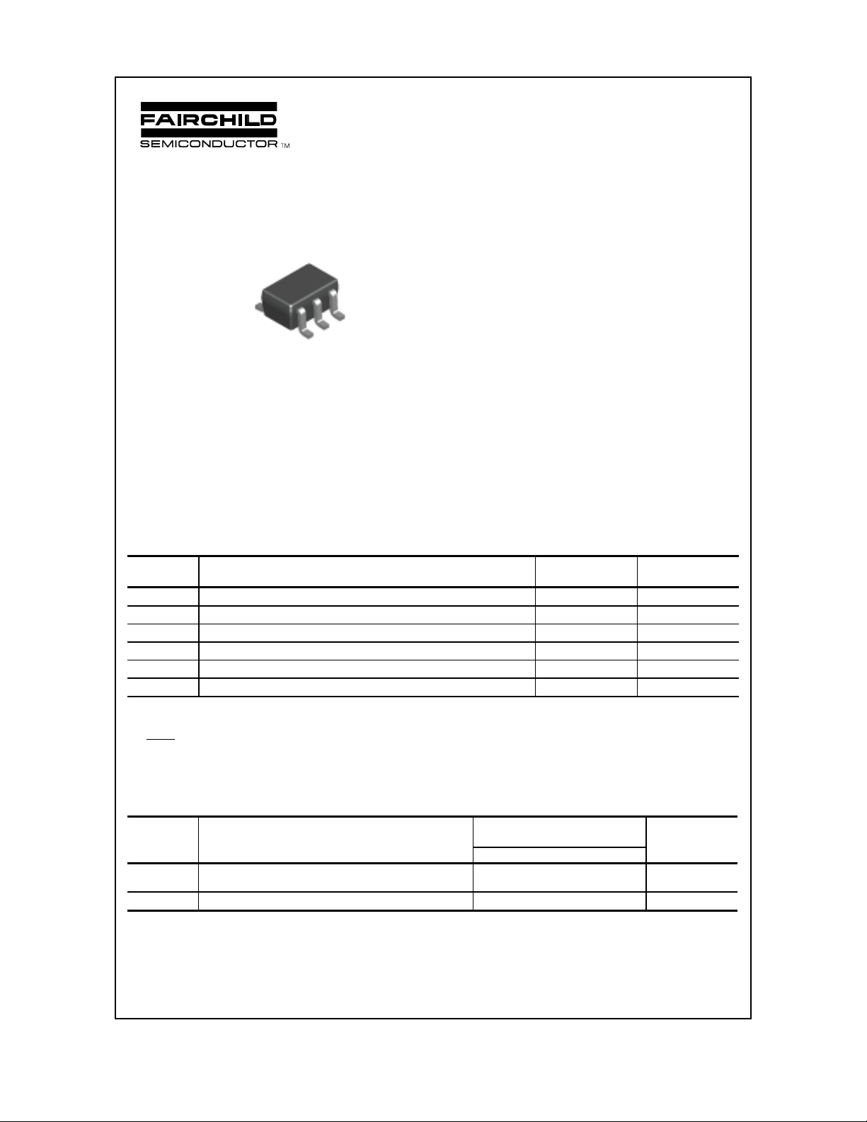
BC847S
SC70-6
Mark: 1C
NOTE: The pinouts are symmetrical; pin 1 and pin
4 are interchangeable. Units inside the carrier can
be of either orientation and will not affect the
functionality of the device.
pin #1
C2
B1
E1
NPN Multi-Chip General Purpose Amplifier
This device is designed for general purpose amplifier applications at collector
currents to 200 mA. Sourced from Process 07.
Absolute Maximum Ratings* T
Symbol Parameter Value Units
V
CEO
V
CES
V
CBO
V
EBO
I
C
TJ, T
stg
*These ratings are limiting values above which the serviceability of any semiconductor device may be impaired.
NOTES:
1) These ratings are based on a maximum junction temperature of 150 degrees C.
2) These are steady state limits. The factory should be consulted on applications involving pulsed or low duty cycle operations.
Collector-Emitter Voltage 45 V
Collector-Base Voltage 50 V
Collector-Base Voltage 50 V
Emitter-Base V ol tage 6.0 V
Collector Current - Continuous 200 mA
Operating and Storage Junctio n Temperature Range -55 to +150
= 25°C unless otherwise noted
A
C
°
4
Thermal Characteristics T
= 25°C unless otherwise noted
A
Symbol Characteristic Max Units
BC847S
P
D
R
JA
θ
2001 Fairchild Semiconductor Corporation Rev.A1
Total Device Dissipation
Derate above 25°C
300
2.4
Thermal Resistance, Junction to Ambient 415
mW
mW/°C
C/W
°
NPN Multi-Chip General Purpose Amplifier
(continued)
BC847S
Electrical Characteristics T
= 25°C unless otherwise noted
A
Symbol Parameter Test Conditions Min Typ Max Units
OFF CHARACTERISTICS
V
(BR)CEO
V
(BR)CES
V
(BR)CBO
V
(BR)EBO
I
CBO
Collector-Emitter Breakdown Voltage IC = 10 mA, IB = 0 45 V
Collector-Base Breakdown Voltage
Collector-Base Breakdown Voltage
Emitter-Base Breakdown Voltage
I
= 10 µA, IE = 0
C
I
= 10 µA, IE = 0
C
I
= 10 µA, IC = 0
E
Collector-Cutoff Current VCB = 30 V, IE = 0
V
= 30 V, IE = 0, TA = 150°C
CB
50 V
50 V
6.0 V
15
5.0
nA
µ
A
ON CHARACTERISTICS
h
FE
V
sat
CE(
V
BE(on)
DC Current Gain IC = 2.0 mA, VCE = 5.0 V 110 630
Collector-Emitter S aturation Voltage IC = 10 mA, IB = 0.5 mA
)
Base-Emitter ON Voltage IC = 2.0 mA, V
= 100 mA, IB = 5.0 mA
I
C
= 10 mA, VCE = 5.0 V
I
C
CE
= 5.0 V
0.58 0.7
0.25
0.65VV
0.77VV
SMALL SIGNAL CHARACTERISTICS
f
T
C
obo
Current Gain - Bandwidth Product IC = 20 mA, VCE = 5.0,
f = 100 mHz
Output Capacitance VCB = 10 V, f = 1.0 MHz 2.0 pF
200 MHz
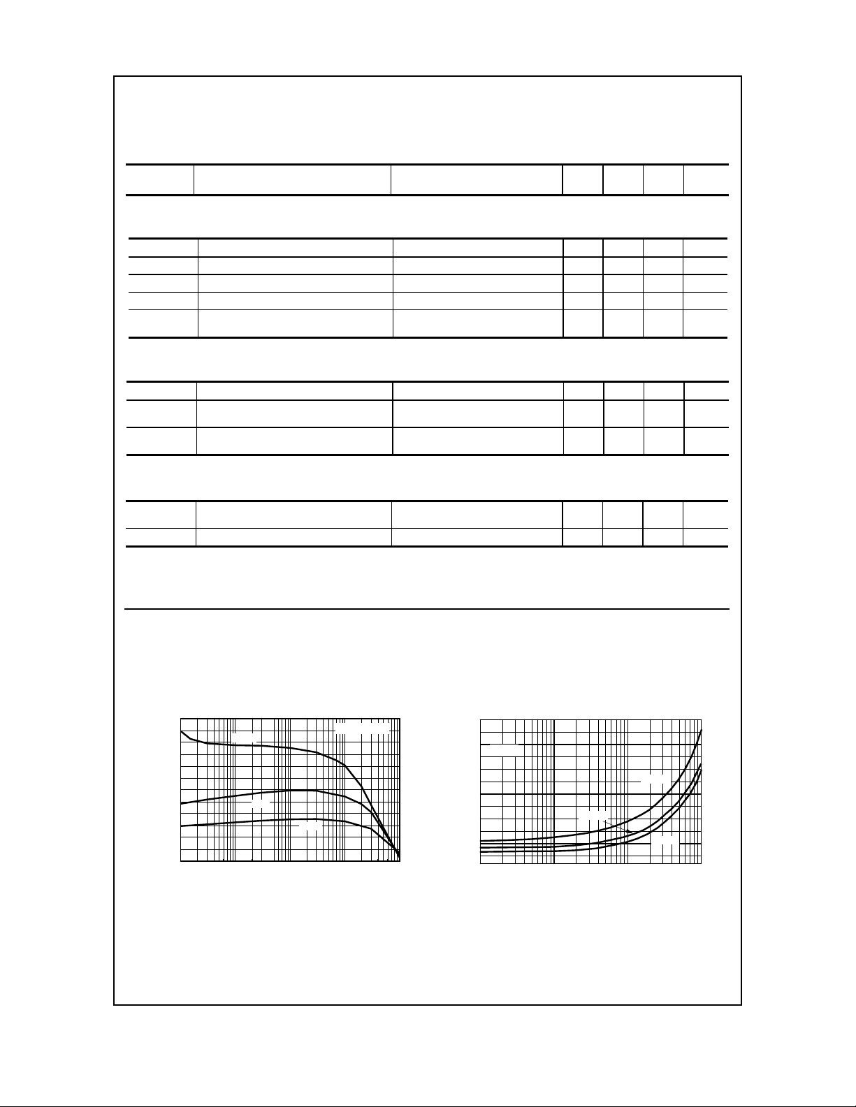
T ypical Characteristics
T ypi c al Pu ls ed Cur rent Ga in
vs Collect or Curre nt
1200
1000
800
600
400
200
0
FE
0.01 0.03 0.1 0.3 1 3 10 30 100
h - TYPICAL PULSED CUR REN T GAI N
125 °C
25 °C
I - COLLECTOR CURRENT (mA)
C
V = 5.0 V
- 40 °C
Collector-Emitter Sat urati on
Voltage vs Collector Curr en t
CE
0.3
0.25
= 10
β
0.2
0.15
0.1
0.05
0.1 1 10 100
CESAT
V - COLLECTOR-EMITTER VOLTAGE (V)
I - COLLECTOR CUR RENT (mA)
C
25 °C
125 °C
- 40 °C
 Loading...