BC847BS
NPN Multi-chip General Purpose Amplifier
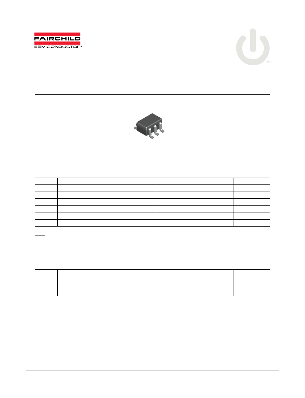
This device is designed for general purpose amplifier applications at collector currents to 200 mA.
Sourced from Process 07.
E2
B2
Dual NPN Signal Transister
SC70-6
Mark: .1F
C1
Pin #1
E1
B1
C2
NOTE: The pinouts are symmetrical; pin 1 and pin
4 are interchangeable. Units inside the carrier can
be of either orientation and will not affect the
functionality of the device.
BC847BS
June 2007
Absolute Maximum Ratings * T
= 25°C unless otherwise noted
a
Symbol Parameter Value Units
V
CBO
V
CES
V
CEO
V
EBO
I
C
T
J, TSTG
* These ratings are limiting values above which the serviceability of any semiconductor device may be impaired.
NOTES:
1) These ratings are based on a maximum junction temperature of 150 degrees C.
2) These are steady state limits. The factory should be consulted on applications involving pulsed or low duty cycle operations.
Thermal Characteristics * T
Collector-Base Voltage 50 V
Collector-Base Voltage 50 V
Collector-Emitter Voltage 45 V
Emitter-Base Voltage 6.0 V
Collector Current (DC) 100 mA
Junction Temperature an d Storage Temperature -55 ~ +150 °C
= 25°C unless otherwise noted
a
Symbol Characteristic Max Units
PD
Total Device Dissipation
Derate above 25℃
R θ JA Thermal Resistance, Junction to Ambient 625 ℃/W
*Device mounted on FR-4 PCB 1.6” X 1.6” X 0.06”.
210
1.6
mW
mW/℃
©2007 Fairchild Semiconductor Corporation 1 www.fairchildsemi.com
BC847BS Rev. A

BC847BS
Electrical Characteristics * T
= 25°C unless otherwise noted
a
Symbol Parameter Test Condition MIN MAX Units
Off Characteristics
V(BR)CBO Collector-Emitter Breakdown Voltage IC = 10 μA, IE = 0 50 V
V(BR)CES Collector-Base Breakdown Voltage IC = 10 μA, IE = 0 50 V
V(BR)CEO Collector-Base Breakdown Voltage IC = 10 mA, IB = 0 45 V
V(BR)EBO Emitter-Base Breakdown Voltage IE = 10 μA, IC = 0 6.0 V
ICBO Collector-Cutoff Current VCB = 30 V, IE = 0
VCB = 30 V, IE = 0, TA = 150°C
15
5.0
On Characteristics
hFE DC Current Gain IC = 2.0 mA, VCE = 5.0 V 200 450
VCE(sat) Collector-Emitter Saturation Voltage * IC = 10 mA, IB = 0.5 mA
IC = 100 mA, IB = 5.0 mA
VBE(on) Emitter-Base Breakdown Voltage * IC = 2.0 mA, VCE = 5.0 V
IC = 10 mA, VCE = 5.0 V
* Pulse Test: Pulse Width≤300μs, Duty Cycle≤2%
NOTE: All voltages (V) and currents (A) are negative polarity for PNP transistors.
0.58 0.7
0.25
0.65
0.77
nA
μA
V
V
V
V
BC847BS Rev. A
2 www.fairchildsemi.com
 Loading...