

Page 1

LZB 115 2508 R1A Technical Descrip ti on
Chapter 3 -Technical Description
Introduction
This chapter describes the technical description and functionality of the CA638 and the CF688 Cellular
Phones.
Features
The CA638 and the CF688 Cellular Phones share the following features:
• 17 key keypad
• System select function with preferred network memory
• Phone security func t i on s:
- SIM with cardlock
- Phone lock option
- Call restrict option
- Keypad lock
- Fixed dialing option
• Four display language options:
- English
-French
-Spanish
- Auto Alternative
• Different ring levels
• Alarm function with snooze option
• AnyKey and Auto answer modes
• Call forward
• Call waiting
• Voice mail
• Call time/cost display
• Calculator
• Conference calling
• Two voice line options (Alternate Line Service)
3-1
Page 2

Technical Description LZB 115 2508 R1A
• 15 last dialed number memory
• 5 number last received memory
• Unanswered call identification
• Send identification option
• Microphone mute
• Scratch pad display
• DTMF capabilities
• Enhanced Speech Quality (EFR)
The CA638 and the CF688 differ in the following areas:
• The CA638 has an interchangeable front keypad cover.
• The Keypa d layout is different for the two phones. See Figure 3-2
and Figure 3-3.
• The CF688 has a larger display area.
• The CF688 includes side volume keys.
• The CF688 includes an active flip.
3-2
Page 3

LZB 115 2508 R1A Technical Descrip ti on
External Components
This section describes the external components of the CA638 and the CF688 Cellular Phones. Figures are
included to identify relevant areas of the phone, and tables explain the function of each component. The
following information is included:
• Figure 3-1
• Figure 3-2
• Figure 3-3
• Figure 3-4
• Figure 3-1
and Table 3-1: External Components of the CA638
and Table 3-2: External Components of the CF688
and Table 3-3: Keypad Components
and Table 3-4: LCD display areas
, Figure 3-2, and Table 3-5: Top Indicator Functions
Figure 3-1. CA638 External Components
NOTE
The rear panel of both version phones is the same. See Figure 3-2.
Table 3-1. CF638 External Components
Fig.
Ref.
1 Antenna
2 Indicator Light
3 Earpiece
4Display
5 Keypad
6 System Connector
7 Microphone
8 Exchangeable Front Panel
Description
3-3
Page 4

Technical Description LZB 115 2508 R1A
3-4
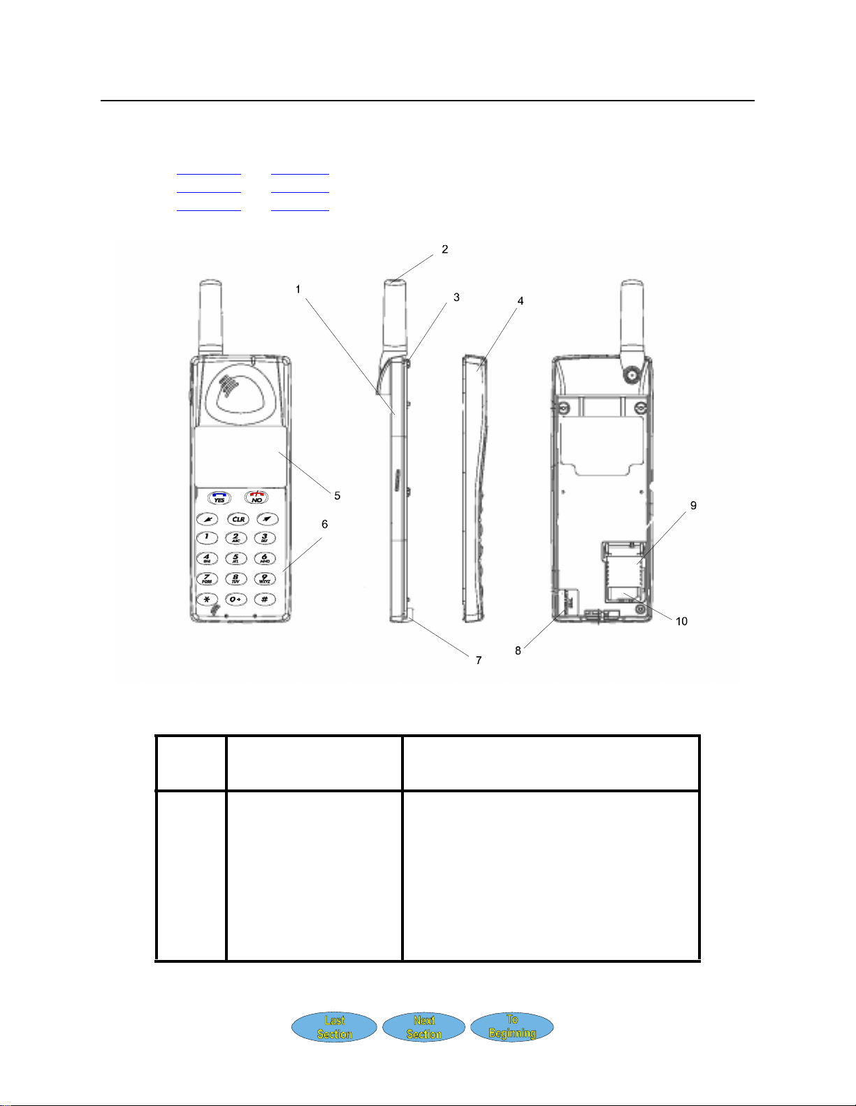
Figure 3-2. CF688 External Components
Table 3-2. CF688 External Components
Fig.
Ref.
Description
1 Antenna
2 Indicator Light
3 Earpiece
4Display
5 Keypad
6 Active Flip
7 Microphone
8 Side Volume Keys
9 External Antenna Connector
10 SIM Card and Holder
11 Warranty Label
Page 5

LZB 115 2508 R1A Technical Descrip ti on
Keypad
See Figure 3-3. The ke ypad is controlled by JOSEFIN and consists of a key switch matrix with four output
columns and five return input rows. Pressing a key generates an interrupt and allows JOSEFIN to detect
that key.
The key switch matrix will cover a maximum of 20 keys, but 5 additional keys can be added to the input
rows to become detected when connected to ground. This method enables use of the On/Off and Volume
Up/Down switches.
Figure 3-3. Keypad Components
3-5
Page 6

Technical Description LZB 115 2508 R1A
Table 3-3. Keypad Components
Key Function
Answers incoming calls.
Confirms menu selections and settings.
Accesses quick menu.
Volume control (CA638 only)
Access and navigate thro ugh menu system.
Scroll through text messages.
Turns phone on and off.
Clears displa y i n st a ndby mode.
Cancels menu selections.
Rejects incoming calls.
Mutes phon e.
Erases digits from display.
Returns pho ne to standb y di s pl ay
Terminates input of security codes.
Confirms selections and settings.
Enters characters # and .
Enters characters * and “p” (pause)
Enters numeric characters and text messages.
LCD
See Figure 3-4 and Table 3-4. The Liquid Crystal Display (LCD) is a 3 by 12 character display where each
character is created by a 5 by 7 d ot matrix. Information to and from the LCD is transferred on a single data
line together with a clock signal. Both are provided by JOSEFIN, who also controls the voltage supply to
the LCD by a pulse width modulated (PWM) signal. The voltage supply to the LCD has to be regulated
quite accurately by the logics to obtain optimum performance in the LCD viewing angle and contrast ratio.
JOSEFIN’s software controls the duty cycle (mark/space ratio) of the PWM output.
These digital pulses generate the negative voltage required by the LCD. Because the voltage supplied to the
LCD is most dependent on the load, voltage variations caused by load fluctuations are reduced by feeding
the voltage to an A/D-input of PATTI, where the voltage is checked by software and regulated to match
pre-defined values.
The A/D input of PATTI also provides temperature compensation of the LCD.
3-6
Page 7
LZB 115 2508 R1A Technical Descrip ti on
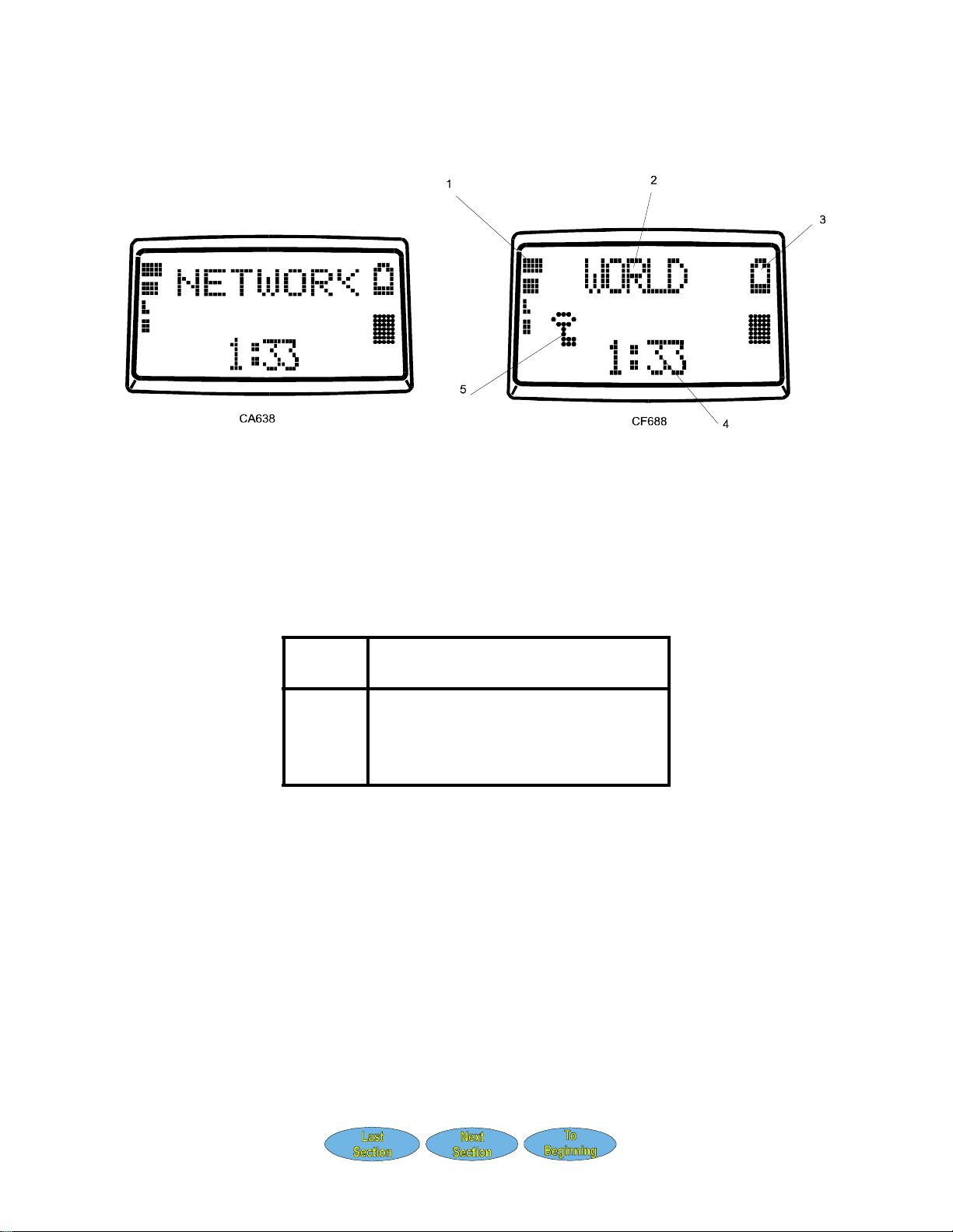
Figure 3-4. LCD Display
NOTE
For more information on displays, refer to the CA638 and the CF688 User Manuals.
Table 3-4. LCD Display Areas
Fig.
Ref.
Description
1 Signal Strength Indicator
2
3
4
5
System Indicator
Battery Strength Indicato r
Time
Keylock Indicator
3-7
Page 8

Technical Description LZB 115 2508 R1A
LEDs
See Figure 3-2 and Table 3-5. The red and gr ee n top LED s are fe d by a no n- flu ctua ti ng su pp ly vo l tage and
are directly controlled by two separate outputs of JOSEFIN. The keypad and LCD illuminations consist of
six and four parallel LEDs, respectively, and are all controlled by a single output from JOSEFIN.
Table 3-5. Top Indicator Functions
Indicator Pattern Function
Slow Blinking Green Phone in standby
Fast Blinking Green Incoming call or message waiting
Blinking Red Low battery warning
3-8
Page 9
LZB 115 2508 R1A Technical Descrip ti on
Internal Components
This section describes the internal components of the CA638 and the CF688.
• See Figure 3-5
• See Figure 3-6
• See Figure 3-7
and Table 3-6 for CA638 internal component locations and descriptions.
and Table 3-7 for CF688 internal component locations and descriptions.
and Table 3-8 for PCB component layout and descript i on.
Figure 3-5. CA638 Internal Components
Table 3-6. CA638 Internal Components
Fig.
Ref. Description Notes
1 Back Cover
2 Antenna
3 Antenna connector
4 Front Cover Includes microphone and loudspeaker
5 Display assembly Includes Light Guide, LCD, LCD Connector
6 Keypad
7 System connector
8 Warranty Label
9SIM Card Holder
10 SIM Connector
Answers incoming calls, lights display
3-9
Page 10

Technical Description LZB 115 2508 R1A
.
3-10
Figure 3-6. CF688 Internal Components
Page 11

LZB 115 2508 R1A Technical Descrip ti on
Table 3-7. CF688 Internal Components
Fig.
Ref. Description Notes
1 Back Cover
2 Antenna
3PCB
See Figure 3-7
and Table 3-8
4 Front Cover
5 Display Assembly Includes Light Guide, LCD, LCD Connector
6 Keypad Answers incoming calls, lights display
7 System Connector
8SIM Card Holder
9 Microphone
10 Microphone Holder
Includes elastomer
11 Active Flip
12 Flip Hinges
13 Side Volume Keys
Dome Foil placed inside front cover assembly
3-11
Page 12

Technical Description LZB 115 2508 R1A
3-12
Figure 3-7. PCB Component Location
Page 13

LZB 115 2508 R1A Technical Descrip ti on
Table 3-8. PCB Component Descriptions
Component Designation Function
Radio:
Pia-Mia N451 Power Control, Amplifier
Edith N500 Quadrature Modulator, I/Q-Filters, Receive IF
Annette E201 Low Noise Amplifier, Down-Converter
T/R Switch V 453 Disables the Transmitter output and enables the
Receiver input
Baud Filter N200 Filters received signals to cut off unwanted frequencies
outside the expected Receive frequency range.
Power Amplifier N400
Harmonic filter N400
Transmit VCO Z250
3.8V Regulator N450
1st channel Filter Z250
2nd Channel Filters
Z500, Z501
A& B
3rd channel Filter Z502
Frequency
N350
Generator
3.8V Regulator N450
Crystal B551
3.2V Regulators N700, N701, N702
Backup capacitor C720
Logics:
Esaiah D900 Speech Encoder
Flash D610
RAM D620
Josefin D600 Central Processing Unit. Channel Encoder, Equalizer,
Interleaving, Ciphering and Deciphering, Deinterleaving, Burst Formatting, Waveform Generator
EEPROM D630
Patti N800 PCM Encoder, Phase Digitizer
SIM Reader
J603
User Interface:
Top Indicator LED H650
Display LEDs H651 - H654
Keypad LEDs H655, H656, H657,
H658, H659, H660
Keypad Switches S00, S02, S03, S10, S11,
S13, S20, S21, S22, S23,
S30, S31, S32, S33, S42,
S43
Active Flip Switch S3
Buzzer H600
Connectors:
Antenna Connector X101
System Connector X602
Side Volume Key
X820
Connector
3-13
Page 14

Technical Description LZB 115 2508 R1A
Functional Description
See Figure 3-8. This section describes the major circuit paths of the CA638 and CF688 Cellular Phones,
and includes the following:
• Logic Paths
• Control Paths
• Connector Information
3-14
Figure 3-8. Block Diagram
Page 15

LZB 115 2508 R1A Technical Descrip ti on
General
All electronic components are integrated into a single board, the Transceiver Board, which is a four-layer
board where the layer assignments are:
• Layer 1: Primary side components and signal paths
• Layer 2: Signal paths
• Layer 3: Ground plane for Digital GND and Analog GND
• Layer 4: Secondary side components and signal paths
The Transceiv er Board is phy s ically and functionally divided i nto two separate electronic bloc ks.
• the Logic block, fr om here on referred t o as the Logics
• the Radio block, from here on referred to as the Radio
The two blocks are mounted in separately shielded cavities and all signals to and from the two blocks are
EMI decoupled to prevent spurious radiation, which makes the phone conform to the current requirements
for radiated spurious transmission.
Most of the signal processing takes place in chips designed by Ericsson. Due to their complexity, these
chips can not be assigned a descriptive name, but are instead given a name. See Figure 3-7
.
Transmission
The Logics block and the Radio block handle the transmission path from microphone to antenna. See Fig-
ure 3-9.
Logic Block
The signal to be transmitted is processed by the following logic blocks:
• PCM Encoder
• Speech Encoder
• Channel Encoder
• Interleaving
• Ciphering
• Burst Formatting
• Waveform Generator
3-15
Page 16

Technical Description LZB 115 2508 R1A
Figure 3-9. Logic Transmission Path
PCM Encoder (P ATTI)
The analog speech signals from the microphone are amplified, then converted to digital shape by an A/Dconverter located in PATTI. The conversion, known as Pulse Coded Modulation (PCM), includes three different steps:
• Sampling (8kHz)
• Quantizing (8192 levels)
• Coding (1 3 bit binary code)
The bit rate delivered by PATTI is 13 bits x 8kHz = 104 kbit/s.
Speech Encoder (ESAIAH)
As the rate of the bit stream from PATTI is too high to handle, the bit rate has to be reduced, which is made
possible as the speech contains portions of redundant information. By slicing the digital speech into segments of 20 ms, the hybrid Speech Encoder of the Digital Signal Processor (DSP) named ESAIAH
removes these redundant portions, as “white noise” is filtered out from the speech. The remaining part, the
filter parameters, will be transmitted and the bit rate is in this way reduced from 104 kbit/s to 13 kbit/s (8:1
compression), i.e. 260 bits for each 20 ms speech segment.
3-16
Page 17

LZB 115 2508 R1A Technical Descrip ti on
Channel Encoder (JOSEFIN)
The BER (Bit Error Rate) should be kept as low as possible. Due to the mobility of a GSM phone, errors
will occur but a certain amount of errors can be allowed if the original information can be restored or in
worst case detected and rejected. By spreading out the information to an increased number of bits, the
Channel Encoder will improve the security against errors. The 260 bits per segment supplied by ESAIAH
are divided by JOSEFIN’s Channel Encoder into three separate groups:
• Group 1: 50 most important bits
• Group 2: 132 important bits
• Group 3: 78 least important bits
• Total: 260 bits
A block coder enlarges the first group with three parity bits. These bits, along with the bits of the second
group plus four tail bits encoded by a convolutional coder at a ratio of 1:2. These bits are added to the
uncoded third group, resulting in a total of (50+3 + 132 + 4) x 2 + 78 = 456 bits per segment or 22.8 kbit/s.
Channel Coding is primarily utilized for detection and correction of single errors and short error bursts.
Interleaving (JOSEFIN)
When it comes to correction of error b ursts with longer duration, the Interleaving section of JOSEFIN will
reduce the risk of continuous error intervals, as consecutive bits in a burst are spread out over several
bursts. Possible error bursts will also be spread out on the reception side.
Ciphering (JOSEFIN)
Speech and data have to become ciphered by JOSEFIN in order to prevent unauthorized parties from getting access to the communication. A message, a ciphering key, and the selected TDMA frame number are
fed through an encryption algorithm and sent to the base station. If successfully decrypted by the base station, all traffic will from here on be ciphered at a 1:1 input/output ratio.
Burst Formatting (JOSEFIN)
There are two kinds of logical channels, control- and traffic- channels, which JOSEFIN maps onto the
physical channels. A physical channel is represented by one of the eight time slots in the TDMA frame,
where a single time slot contains the information of one burst. A normal burst starts and ends with three tail
bits and consists of two blocks with 57 encrypted bits plus one flag bit each with a Training Sequence (a bit
pattern known by the receiving station) of 26 bits between, for a total of 148 bits. The duration of a time
slot is 0.577 ms corresponding to 156 bits. The eight redundant bits will become a “safety zone” against
time slot overlapping. Burst Formatting will increase the bit rate from 22.8 to 33.8 kbit/s.
Waveform Generator (JOSEFIN)
The digital information of the time slot bursts has to become converted to baseband signals by the Waveform Generator, which is the final stage of JOSEFIN. The digital outputs of the Waveform Generator are
derived from lookup tables to generate a bit stream output from one-bit D/A-converters, which supplies the
Radio Transmitter with the two vector information signals I and Q (In-phase and Quadrature-phase,
respectively).
3-17
Page 18

Technical Description LZB 115 2508 R1A
Radio Block
The transmit and receive paths are always kept apart. The Radio includes however three oscillating devices
utilized for transmission as well as reception:
• VCXO (Voltage Controlled Crystal Oscillator) includes a 13MHz crystal and this frequency is distributed to:
-the Logics as main clock
-the QVCO as reference frequency
-the Frequency Generator of the Synthesizer as reference frequency
• QVCO (Quadrature Voltage Controlled Oscillator) is able to provide multiples of the 13MHz frequency for:
-the TX IF (Intermediate Frequency)
-the RX IF (Intermediate Frequency)
• Synthesizer, consisting of a phase-locked Frequency Generator and LVCO (Local Voltage Controlled Oscillator), operating at 200kHz carrier separation intervals for generation of frequencies
required by:
-the TX up-convert er
-the RX down-converter
3-18
Figure 3-10. VCXO, QVCO, and Synthesizer
Page 19

LZB 115 2508 R1A Technical Descrip ti on
See Figure 3-11. The following radio blocks process the transmitted signal:
• I/Q-Filters
• Quadrature Modulator
• Up-Converter
• Power Control & Amplifier
• Harmonic Filter
• Antenna Switch
Figure 3-11. Radio Transmission Path
I/Q-Filters (EDITH)
The base-band signals I and Q generated by the waveform generator of JOSEFIN have to become filtered
by low-pass filters in order to remove the quantization noise without affecting the actual information.
Quadrature Modulator (EDITH)
The Quadrature Modulator of EDITH modulates the I/Q-signals by an Intermediate Frequency (IF) from
the QVCO, resulting in a phase modulated signal with a frequency identical to the IF.
Up-Converter
The Quadrature Modulator output is connected to the reference input of a Phase Detector where the output
is fed to a voltage-controlled oscillator (TXVCO). The output frequency of this oscillator is subtracted
from the frequency of the Synthesizer (LVCO) in a mixer and fed back to the second input of the Phase
Detector. This phase-locked loop forces the oscillator to follow the phase of the modulated signal at the
requested frequen cy determined by the Synthesizer. The Synthesize r output pro vides freq uencies (LVCO)
in intervals identical to the carrier separation 200kHz, depending on the frequency to be transmitted. The
Transmit Frequency (TX) is obtained by subtracting the TX Intermediate frequency (TXIF) supplied by the
QVCO from the Synthesizer frequency (LVCO).
3-19
Page 20

Technical Description LZB 115 2508 R1A
Power Control (PIA-MIA) & Amplifier
The output signal from the up-converter has to be amplified to a maximum power level prior to being transmitted from the antenna. As the power level has to be adjusted to the momentary transmission conditions,
the phone must be able to transmit at 16 different power levels, which requires the output power to be controlled in a rather strict way by the power control circuitry of PIA-MIA. The output power from the amplifier is controlled by a feed back loop. A voltage proportional to the battery current supplied to the amplifier
is fed back to a voltage regulator, which makes it possible for the power detector of PIA-MIA to detect an
extremely wide ra nge of outp ut power leve ls.
Harmonic Filter
The harmonics created by the non-linear behavior of the Power Amplifier are removed from the carrier frequency with the help of a low-pass harmonic filter.
Antenna Switch
A PIN diode switch keeps the Transmitter separated from the Receiver. The bit rate when transmitted “on
the air” is approximately 270 kbit/s.
Reception
See Figure 3-12. Received information is picked up by the antenna and directed with the help of the
antenna switch to the Receiver, consisting of the Radio, followed by the Logics, and ended with the earpiece.
3-20
Page 21

LZB 115 2508 R1A Technical Descrip ti on
Radio
See Figure 3-12. The following radio blocks process the received signal:
• Antenna Switch
• Band Filter
• Low Noise Amplifier (ANETTE)
• Down-Converter (ANETTE)
• First Channel Filter
• RX-IF (EDITH)
Figure 3-12. Radio Reception Path
Antenna Switch
The PIN diode switch disables the Transmitter output and enables the Receiver input.
Band Filter
The signal received by the antenna is filtered by a band filter to cut off unwanted frequencies outside the
expected RX frequency range.
Low Noise Amplifier (ANETTE)
The received signal is amplified by a Low Noise Amplifier prior to frequency down-conversion the.
Down-Converter (ANETTE)
The RX frequency has to be amplified and down-converted to a fixed frequency. The Synthesizer output
provides frequencies (LVCO) in 200 kHz intervals. The RX frequency, which is somewhat higher than the
corresponding TX frequency due to duplex separation, is fed together with the Synthesizer frequency
LVCO to a mixer where the output, the 1
LVCO fro m RX.
st
Intermediate Frequency (1st IF), is obtained by subtracting
3-21
Page 22

Technical Description LZB 115 2508 R1A
First Channel Filter
As the signal delivered by the down-converter is a differential IF output signal, the First Channel Filter is
differential as well with a frequency identical to the 1
st
IF.
RX-IF (EDITH)
The filtered 1st IF receive signal is fed to EDITH, where it is preamplified, limited by a limiting amplifier
and fed to the input of a mixer. The second mixer input is a fixed frequency provided by the QVCO. A sec-
ond intermediate frequency (2
nd
IF) of 6 MHz is generated by subtracting the QVCO from the 1st IF. The
6MHz 2nd IF signal inside EDITH passes through two additional limiting amplifiers being preceded by
one dual and one single external 6 MHz channel filter responsible. The three limiting amplifiers are
equipped with amplitude detectors, utilized by the Logics for Received Signal Strength Indicator (RSSI)
calculations. The three amplitude signals are, together with the differential 2
nd
IF signal containing the RX
phase information, fed to the Logics for A/D-conversion and digital processing.
Logics
See Figure 3-13. The following logic blocks process the received signal:
•
Phase Digitizer (PATTI)
• Equalizer (JOSEFIN)
• Deciphering (JOSEFIN)
• Deinterleaving (JOSEFIN)
• Channel Decoder (JOSEFIN)
• Speech Decoder (ESAIAH)
• PCM Decoder (PATTI)
3-22
Figure 3-13. Logic Reception Path
Page 23

LZB 115 2508 R1A Technical Descrip ti on
Phase Digitizer (PATTI)
The differential RX-IF signal from the Radio is a hard limited phase modulated signal, which has to be
converted from analog to digital shape. The 6 MHz input signal is sampled at 13 MHz and transformed to
digital data by the Phase Digitizer of PATTI.
Equalizer (JOSEFIN)
Reflections from distant object, so-called time dispersion, will cause interference problems for the receiver
which are difficult to correct, unless the receiver is adapted to a channel model. The receiver is adjusted to
a particular mathematical channel model as the Equalizer creates a model of the air interface and also calculates the most probable transmission sequence. The Equalizer uses the known Training Sequence
inserted into the middle of the bursted data to create the channel model. The model fluctuates continuously
but is regarded to be stable during one burst.
Deciphering (JOSEFIN)
The speech and data ciphered by the transmitting station must become deciphered by JOSEFIN prior to
further reception processing. All bits are at this point reassembled into the original 456-bit messages.
Deinterleaving (JOSEFIN)
The consecutive bits spread out over several bursts by interleaving of the transmitting station have to be
reinstalled into their proper positions, i.e. deinterleaved by JOSEFIN. Deinterleaving spreads the “damaged” bits of an error burst become spread out during a longer period, which improves the possibility of a
correction recovery.
Channel Decoder (JOSEFIN)
The Channel Decoder of JOSEFIN decodes each 456-bit message for error detection and correction. The
first decoding is performed by a Convolutional Decoder, where 378 bits are decoded and reduced to 187
bits, fed to the Block Decoder which looks for error frames being indicated at the output as Bad Frame
Indications (BFIs). These 187 bits (53 Most Important Bits + 132 Important Bits) are added to the remaining Least Important 78 bits, resulting in a total of 260 bits per 20ms segment (13kbit/s), which are fed from
JOSEFIN to the Digital Signal Processor (DSP) called ESAIAH.
Speech Decoder (ESAIAH)
The hybrid Speech Decoder of ESAIAH processes the incoming filter parameters of the speech information, resulting in a 1:8 decompression, i.e. a bit rate increase from 13kbit/s to 104kbit/s.
PCM Decoder (P ATTI)
The Pulse Coded Modulation (PCM) decoder of PATTI consists primarily of a D/A-converter, where the
digital 104 kbit/s “speech” is transformed into an analog AC-voltage, which after being amplified and supplied to the earpiece, will be able to reproduce the voice of the transmitting party.
3-23
Page 24

Technical Description LZB 115 2508 R1A
Central Processing Unit JOS EFIN
See Figure 3-14. JOSEFIN is the central processing unit of the transceiver and contains among other things
a CPU with Subsystem, internal RAM, Timing Generator for the TDMA structure, and a Real Time Clock
(RTC). The RTC, which also handles the alarm function, is active as long as the battery is connected. After
disconnecting the battery the RTC is still active for more than 72 hours due to a backup capacitor.
Apart from taking significant part in the transmit/receive signal process ing, JOSEFIN also controls the following peripheral functions and devices:
• Battery Charging
• Power Distribution
• System Connector
• Key Switches
• Memories (RAM, FLASH, EEPROM)
• SIM-card
• Indicators (LCD, LEDs, Buzzer)
• Radio Interface
3-24
Figure 3-14. Central Processing Unit JOSEFIN Peripherals
Page 25

LZB 115 2508 R1A Technical Descrip ti on
Battery Charging
See Figure 3-15. The battery charging is a rather complex algorithm where several of the numerous parameters are stored in an EEPROM in case of future adjustments. JOSEFIN controls the charging current to the
attached battery by altering the duty-cycle of a control signal which, via PIA-MIA, affects a transistor
switch that supplies current to the battery from an external charger. For proper duty-cycle regulation,
JOSEFIN requires a feedback value of the actual current. This value is provided as a voltage by PIA-MIA
and delivered to JOSEFIN after being A/D-converted by PATTI. This signal also detects when a charger is
connected, as this will generate an offset voltage at the PIA-MIA output.
Figure 3-15. Battery Charging Block Diagram
Chargers
The external charger can be a DC/DC-converter or a full-wave rectified AC/DC-converter, regulated or
non-regulated. Whenever a charger is connected to the phone a charging cycle is initiated, even if the phone
is off, due to the auto turn on feature. The charging is temporarily halted when a call is in progress, except
when the battery voltage is low.
Batteries
The batteries being used are four 1.2V cell Nickel-Metal-Hydride (NiMH) or Nickel-Cadmium (NiCd)
chargeable batteries without internal thermistor. Refer to Chapter 6
for more information.
3-25
Page 26

Technical Description LZB 115 2508 R1A
Temperature Guard
An on-board thermistor generates a temperature-related voltage, which after being A/D-converted by
PATTI, is registered by JOSEFIN. If the temperature during charging exceeds a certain level, charging is
halted until the temperature has dropped to a specific level, and charging is resumed. If the temperature
rises a second time, charging is terminated. After attaching a battery to the phone, the thermistor has to be
able to detect an abnormal battery temperature in order to protect the battery from being charged at out-ofrange temperatures. Charging is commenced after a few minutes delay, if the temperature is found to be
stable. If not, a longer delay will be introduced.
Charging Complete
The charging cycle can be terminated in four different ways:
• Minus delta v (normal): The battery voltage is sampled once a second for approximately one
minute and the mean value is calculated. The maximum mean value is stored and compared with
consecutive mean values. When a specific divergence is obtained, charging is terminated.
• Peak detect: The charging is terminated when the above mentioned mean values are less or identical to the maximum mean value for a specific time.
• Overvoltage detection: If PIA-MIA detects battery overvoltage a specific number of times during a
charging cycle, charging is terminated.
• Safety timer: The safety timer function is used as a last resort when the other methods do not work.
The phone trickle charges the battery after th e main charge is completed, until the charger is disconnected.
The phone also protects the battery from becoming overcharged by checking charge status at the start of
charging. If the battery has a full charge, the phone terminates charging, and maintains trickle charge. The
phone also has a timer which regulates charging.
The timer is started when the charger is disconnected. The time setting varies depending on whether the
phone is in standby or serving a call.
3-26
Page 27

LZB 115 2508 R1A Technical Descrip ti on
Power Distribution
See Figure 3-16. Power to the phone can be supplied in two ways:
• From a 4.8V, 4-cell NiMH or NiCd main battery
• From an external power source attached to the system connector (battery has to be attached)
Power On/Off
The power on/off function is initiated by pressing the On/Off (NO) key.
Power On
The battery voltage is connected to the On/Off switch, which after being pressed, enables and activates a
number of voltage regulators. The voltage from the On/Off-switch is detected by JOSEFIN, which activates an output connected to the enable inputs of the regulators, to keep the regulators active after the On/
Off switch has been released.
Figure 3-16. Power On and Off
Power Off
Pressing the On/Off-switch again will not affect the enable inputs of the voltage regulators, but will be
detected by the voltage from the On/Off-switch to the input of JOSEFIN, which first terminates the program in a co ntrolled w ay and then disables the r egulators, using the same output as for power on.
Auto Turn On
If the phone is off when a charger is connected, the Auto Turn On feature will automatically initiate charging.
3-27
Page 28

Technical Description LZB 115 2508 R1A
Voltage Regulators
The Transceiver Board includes a number of linear voltage regulators for the Logics as well as for the
Radio.
Logic Voltages
The voltages to the Logics are supplied by three 3.2 V linear regulators plus one 3.5 V regulator to the following four groups of circuits:
• JOSEFIN, Memories, LCD
•ESAIAH
•PATTI
• Real Time Clock in JOSEFIN (supplied with 3.5 V whenever a battery is attached to the phone)
A DC/DC converter is also utilized in order to generate the 5 V required by the SIM-card. This voltage is
also supplied to the system connector interface.
Radio Voltages
The Radio includes three 3.8 V linear voltage regulators and one reset and error flag generator, all integrated into one chip. The three voltages are enabled/disabled by JOSEFIN in the same way as the th ree regulators on the Logic side. Two of the three regulators provide supply voltages for the Radio circuits, while
the third one is utilized by the Logics:
• ANETTE, PIA-MIA, EDITH
• Synthesizer, EDITH
• Radio Interface of JOSEFIN, Buzzer, Top LEDs
The combined power reset and error flag output is also connected to JOSEFIN for two purposes:
• The power reset generates the required H/W-reset during the start-up procedure
• The error flag will switch off the phone if the voltage drops below 3.55 V
3-28
Page 29

LZB 115 2508 R1A Technical Descrip ti on
Memories
Three different kinds of external memories are connected to and controlled by JOSEFIN:
• RAM
• FLASH
• FLASH
RAM
The RAM is a Static Random Access Memory (SRAM) with a memory size of 2 k (8 bits). Its address and
data bus plus Write Enable control bit are shared with the Flash memory.
FLASH
The FLASH memory is a 1024 k (8-bit) which stores the program code. This code can be and re-programmed at production and service via the system connector. Data to the FLASH memory is transferred on
the serial link TTMS. Programming voltage is connected to VPPFLASH. Programming is controlled by
the RAM.
EEPROM
The memory size of the Electrically Erasable PROM (EEPROM) is 8 k (8 bits). Bi-directional data is not
transferred on a parallel data bus but on a two wire serial bus, clock and data, which are shared with the
LCD.
SIM-Card
JOSEFIN communicates with he SIM card on a serial bi-directional data wire with the help of a synchronizing clock signal. JOSEFIN also provides a reset output and power enable output for the SIM-card.
3-29
Page 30

Technical Description LZB 115 2508 R1A
Indicators
JOSEFIN controls three different kinds of indicators:
• LCD (Liquid Crystal Display)
• LEDs (Light Emitting Diodes)
• Buzzer
Buzzer
The buzzer is supplied with the same non-fluctuating voltage as the top LEDs and is controlled by a tone
generator output of JOSEFIN.
Radio Interface
The communication between JOSEFIN and the Radio includes not only TX and RX signals but also a vast
number of control signals, all together 33 signal lines. Some signals have to become A/D- or D/A-converted, which is effected by PATTI.
System Connector
The System Connector interfaces the phone with external peripherals and controls battery charging. See
Figure 3-17
and Table 3-9 for more inform ati on .
Figure 3-17. System Connector
3-30
Page 31

LZB 115 2508 R1A Technical Descrip ti on
Table 3-9. System Connector Pin Signals
Pin Signal Designation Function
1 AFMS PATTI Out Audio From Mobile Station
2 ATMS PATTI In Audio To Mobile Station
3 EXTAUD JOSEFIN In External Analog Audio Accessory Sense
4 AGND Audio Signal Ground, 0V reference
5 PORTHF JOSEFIN In Portable Handsfree
6 MUTE JOSEFIN Out Music Mute
7 VPPFLASH Flash In Flash Memory Voltage and Service Voltage
8 VDD Voltage Out Logic Reference, Status ON
9 TFMS/
DFMS
JOSEFIN Out Terminal Ad ap ter Equipment From
Mobile Station/Data From Mobile Station
10 GND Digital Ground and DC Return
11 TTMS/
DTMS
JOSEFIN In Terminal Adapter Equipment To Mobile
Station/Data To Mobile Station
12 DCIO Voltage In/Out DC positive pole for phone battery charging
and external accessory power.
3-31
Page 32

Technical Description LZB 115 2508 R1A
Specifications
General
Frequency Ra nge
Channel Spacing 200kHz
Modulation GMSK
TX Phase Accuracy <5 Ω RMS phase error (burst)
Duplex Spacing 80MHz
Frequency Stability ±5ppm (downlink RX)
LCD 5 x 7 dot matrix
Keypad 17 front keys
Antenna Quarter-wave
External Antenna Jack Yes
Voltage Operation +4.8V
Power Consumption Conversation: 275mA (100% speech,
Battery Durability High performance: 260 min. talktime
TX: 1850 - 1910 MHz
RX 1930 - 1990 MHz
full rate speech coding)
Standby: 12/15mA (incl./excl. SIM-sup-
port clock stop mode)
(100% speech, full rate speech coding)
High capacity: 215 min. talktime (100%
speech, full rate speech coding)
3-32
Ultra slim: 140 min. talktime (100%
speech, full rate speech coding)
Slim: 105 min. talktime (100% speech,
full rate speech coding)
Dimensions 130 x 49 x 13 mm (excl. battery)
Weight 95g (excl. battery)
Temperature Range -10 ° to +55 ° C (operating)
-40° to +85° C (stora ge )
0° o +35° C (charging)
Humidity 0 - 95% relative humidity
Page 33

LZB 115 2508 R1A Technical Descrip ti on
Tran smitter
RF Power Output 30dBm ± 2dBm, Class 1 (1W peak)
Output Impedance 50Ω
Spurious Emission -36dBm below 1GHz; <-30dBm
above1GHz
Receiver
RF Level -105dBm
RX Bit Error Rate < 2%
3-33
Page 34

Technical Description LZB 115 2508 R1A
3-34
 Loading...