

Page 1

SED1220
LCD Controller/Drivers
Technical Manual
Page 2

Contents
OVERVIEW .........................................................................................................................................................2–1
FEATURES..........................................................................................................................................................2–1
BLOCK DIAGRAM .............................................................................................................................................. 2–2
CHIP SPECIFICATION........................................................................................................................................2–3
DESCRIPTION OF PINS ................................................................................................................................... 2–11
FUNCTIONAL DESCRIPTION ..........................................................................................................................2–14
COMMAND ........................................................................................................................................................ 2–21
CHARACTER GENERATOR.............................................................................................................................2–24
ABSOLUTE MAXIMUM RATINGS ....................................................................................................................2–31
DC CHARACTERISTICS...................................................................................................................................2–32
TIMING CHARACTERISTICS ...........................................................................................................................2–34
MPU INTERFACE (REFERENCE EXAMPLES) ...............................................................................................2–37
INTERFACE TO LCD CELLS (REFERENCE) ..................................................................................................2–38
LIQUID CRYSTAL DRIVE WAVEFORMS (B WAVEFORMS) ..........................................................................2–42
SED1220
– i –
Page 3

SED1220
OVERVIEW
SED1220 is a dot matrix LCD controller/driver for
character display. Using 4bits data, 8bits data or serial
data being provided from the micro computer, it displays
up to 36 characters, 4 user defined characters and up to
120 symbols.
Up to 256 types of built-in character generator ROMs are
prepared. Each character font is consisted of 5 × 8 dots.
It also contains the RAM for displaying 4 user defined
characters each font consisting of 5 × 8 dots. It is symbol
register allows character display with high degree of
freedom. This handy equipment can be operated with
minimum power consumption with its low power
consumption design, standby and sleeping mode.
FEATURES
• Built-in data display RAM – 36 characters + 4 user
defined characters + 120 symbols.
• CG ROM (For up to 256 characters), CG RAM (for 4
characters) and symbol register (for 120 symbols).
• No. of display digit and lines
< In normal mode >
1
(12 digits + 4 segments for signal) × 3 lines + 120
symbols + 5 static symbols (SED1220D
2
(12 digits + 4 segments for signal) × 2 lines + 120
symbols + 5 static symbols (SED1221D**)
3
12 digits × 2 lines + 120 symbols + 5 static symbols
(SED1222D
4
(12 digits + 4 segments for signal) × 2 lines + 120
)
**
symbols + 10 static symbols (SED122AD
< In standby mode >
1
5 static symbols
2
5 static symbols
3
5 static symbols
4
10 static symbols
)
**
)
**
• Built-in CR oscillation circuit (C and R contained)
• Accepts external clock input
• High-speed MPU interface
Affords interface with both 68/80 system MPUs
Affords interface through 4 bits and 8 bits
• Affords serial interface
• Character font consists of 5 × 8 dots
1
• Duty ratio
1/26 (SED1220D**)
2
1/18 (SED1221D**, SED1222D**)
• Simplified command setting
• Built-in power circuit for driving liquid crystal
Power amplifier circuit, power regulation circuit and
voltage followers × 4
• Built-in electronic volume function
• Low power consumption
80 µA max. (In normal operation, including
operating current of the power
supply).
20 µA max. (In standby mode for displaying
static icon).
5 µA max. (In sleeping mode when display
is turned off).
• Power supply
DD - VSS –2.4 V ~ –3.6 V
V
DD - V5 –4.0 V ~ – 6.0 V
V
• Temperature range for wide range operation
Ta = –30 ~ 85°C
• CMOS process
• Shipping style
Chip (Al pad product) SED1222D
Chip (Au bump product) SED122*D
TCP SED122*T
A
*
B
*
**
• This unit does not employ radiation protection design
SED1220
EPSON 2–1
Page 4
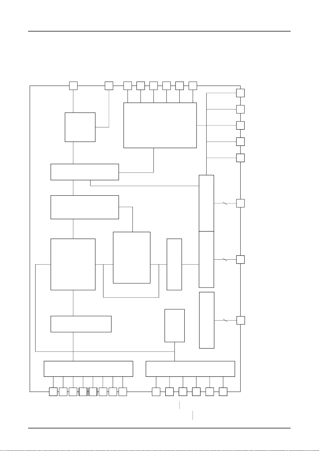
SED1220
Input buffer
MPU interface
Address counter
Command
decoder
Cursor control
SEG driving circuit
Static icon drive circuit
COM driving circuit
Refresh address counter
DD RAM
symbol
register
CG ROM
CG RAM
Timing generatinon circuit
Oscillator
LCD power circuit
IF
RES
CS
WR (E)
P/S
A0
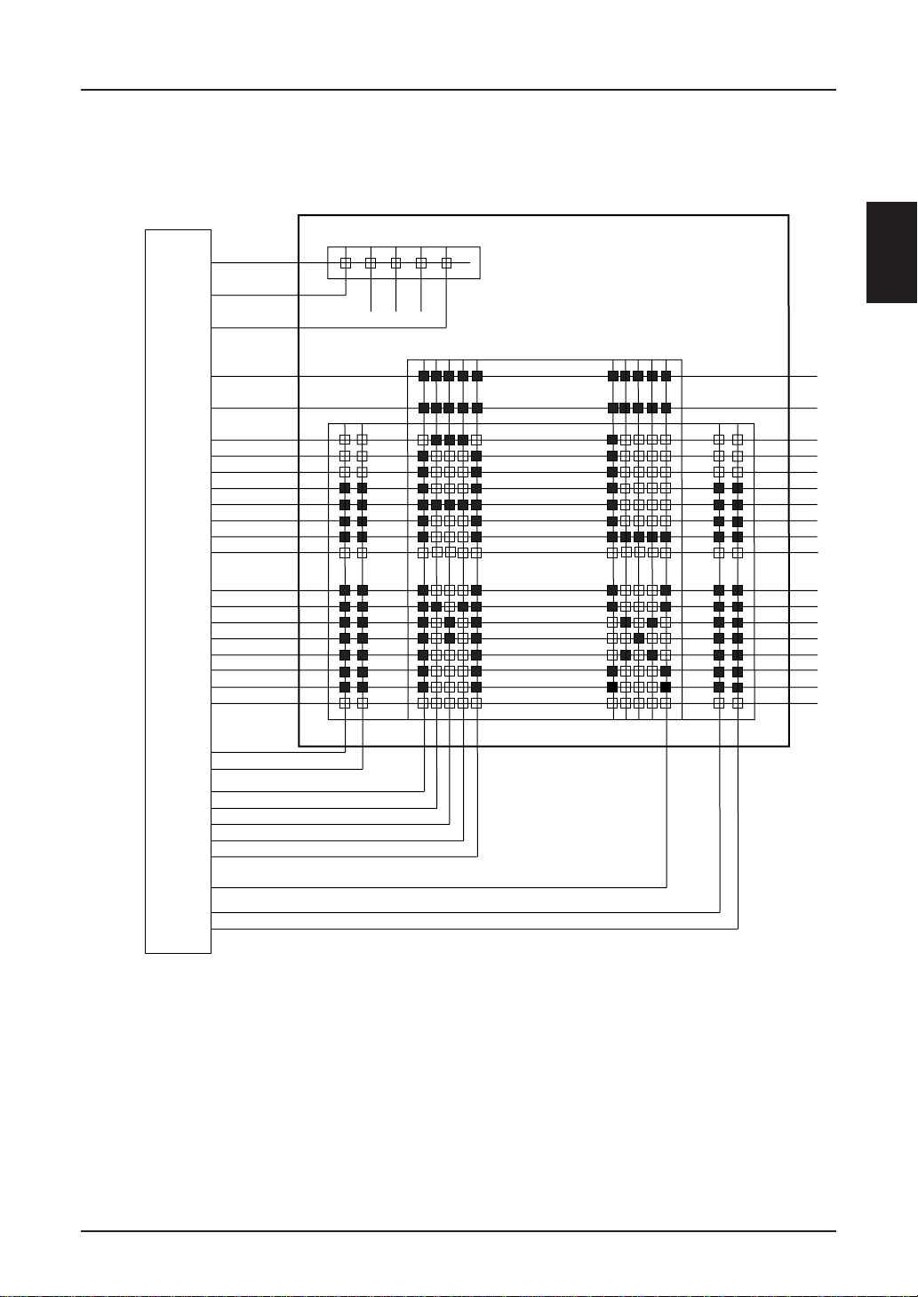
SEG1~60
SEGS1, 2, 4, 5
COMSA
SEGSA, B, C, D, E
SEGSA, B, C, D, E,
F, G, H, I, J (SED122A)
COM1~24
(SED1220/1221)
COM1~16
(SED1222/122A)
COMS1, 2
V
1
V
2
V
3
V
4
V
5
CAP1+CKCAP1–
CAP2+
CAP2–
V
R
V
OUT
V
S1
D6 (SCL)
D0D1D2
D3
D4
D5
D7 (SI)
BLOCK DIAGRAM
2–2 EPSON
Page 5

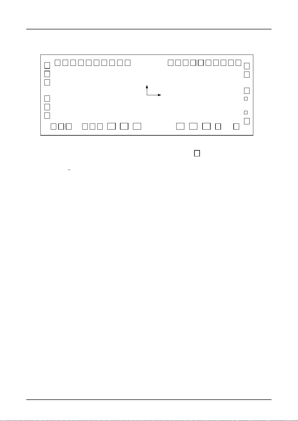
CHIP SPECIFICATION
SED1220D**/1221D**/122AD
146
SED1220
**
74
147
165
1
SED122*D
**
↑
Digits prepared for CGROM pattern changes
Chip size: 7.70 × 2.77 mm
Pad pitch: 100 µm (Minimum)
Chip thickness (for reference): 625 ± 25 µm (SED122
1) A1 pad specifications
Pad size on Y side: 75 µm ×135 µm
Pad size on X side: 135 µm × 75 µm
2) Au bump specifications
Bump size on Y side: 69 µm × 129 µm
Bump size on X side: 129 µm × 69 µm
Bump height (for reference) 22.5 µm ± 5.5 µm
(SED122*D
*
73
SED1220
63
62
56
55
54
:DUMY PAD
:PAD
D
)
A
*
B
)
*
<Fuse Pines>
1) Al pad. pad size 86 µm × 75 µm
2) Au bump
Bump size 80 µm × 69 µm
EPSON 2–3
Page 6
SED1220
SED1222D
109
. . .
125
SED1222D
**
108 52
. . . . . . . . .
y
x
Top View
. . . . . .
12 27
111
**
↑
Digits prepared for CGROM pattern changes
Chip size: 7.70 × 2.77 mm
Pad pitch: 124 µm (Minimum)
Chip thickness (for reference): 625 ± 50 µm (SED1222D
. . . . . . . . .
28 32
: PAD
A
)
*
51
. . .
41
40
. . .
34
33
1) A1 pad specifications
Pad size on Y side: 90 µm × 96 µm
Pad size on X side: 96 µm × 90 µm (PAD. No. 1 ~ 11, 28 ~ 32, 52 ~ 108)
175 µm ×135 µm (PAD. No. 12 ~ 27)
<Fuse Pines>
1) Al pad. pad size 86 µm × 75 µm
2–4 EPSON
Page 7
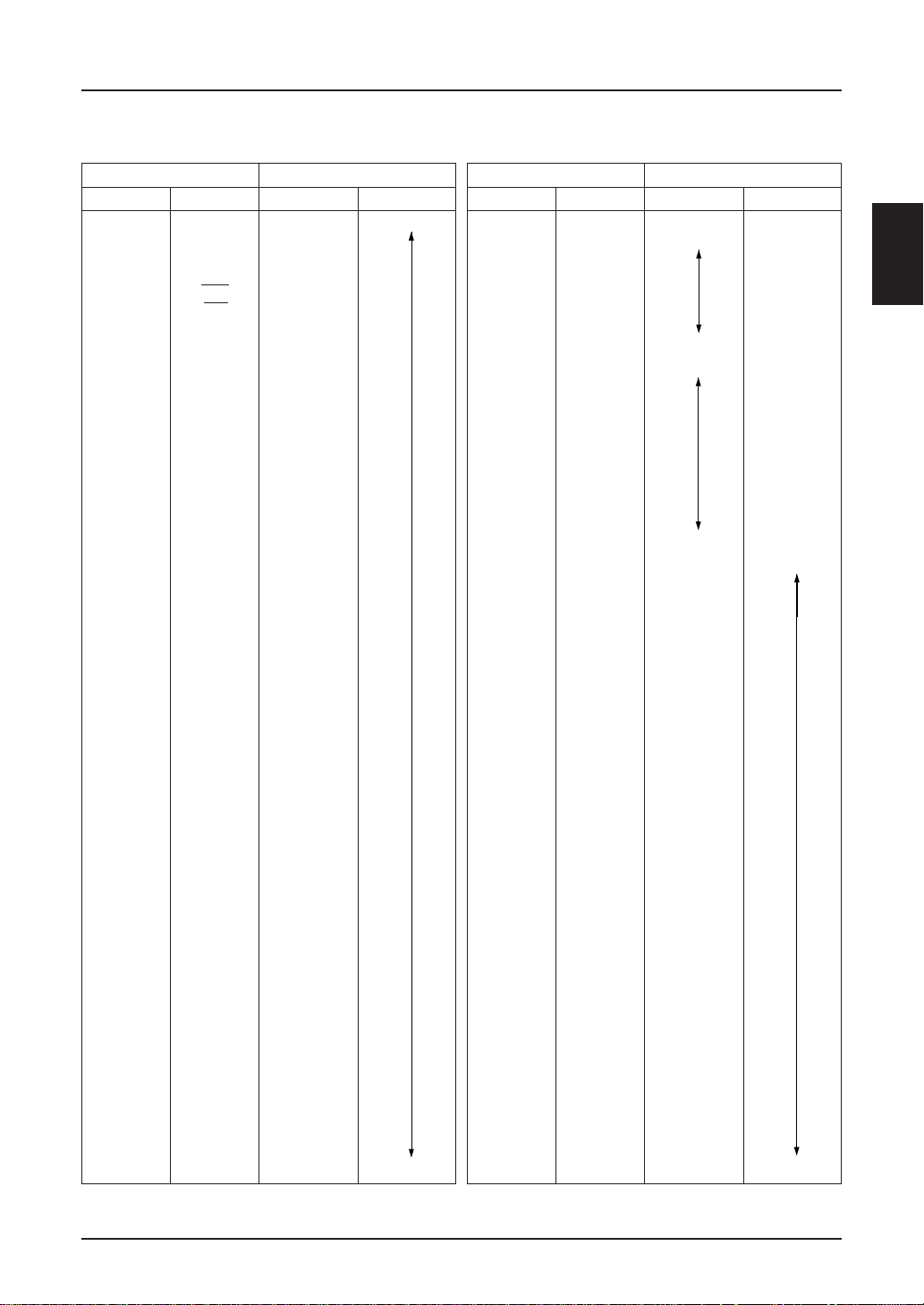
SED1220
<SED1220D**/1221D**>
PAD COORDINATES
No. Name X Y
1 NC –3700 –1204
2 NC –3600
3 NC –3500
4 A0 –3252
5 WR –3132
6 CS –3012
7 D7 –2892
8 D6 –2772
9 D5 –2652
10 D4 –2532
11 D3 –2412
12 D2 –2292
13 D1 –2172
14 D0 –2052
15 V
16 V
17 VSS –1556
18 V
19 V
20 V5 –1176
21 V
22 V
23 V3 –716
24 V
25 V
26 V
27 V1 –156
28 V
29 V
30 V0 224
31 V
32 V
33 VOUT 684
34 V
35 CAP2– 964
36 CAP2– 1064
37 CAP2+ 1244
38 CAP2+ 1344
39 CAP1– 1524
40 CAP1– 1624
41 CAP1+ 1804
42 CAP1+ 1904
43 V
44 V
45 VDD 2364
46 V
47 CK 2693
48 VS1 2821
49 P/S 2949
50 I/F 3077
51 RES 3205
52 NC 3500
53 NC 3600
54 NC 3700 –1204
DD –1836
DD –1736
SS –1456
5 –1276
4 –996
4 –896
3 –616
2 –436
2 –336
1 –56
0 124
R 404
R 504
OUT 784
SS 2084
SS 2184
DD 2464
Unit: µm
PAD COORDINATES
No. Name X Y
55 VDD 3670 –910
56 (FSA) 3603 –796
57 (FSB) –696
58 (FSC) –596
59 (FS0) –496
60 (FS1) –396
61 (FS2) –296
62 (FS3) 3603 –196
63 V
DD 3670 –82
64 COMSA 61
65 COMS1 203
66 COM1 303
67 COM2 403
68 COM3 503
69 COM4 603
70 COM5 703
71 COM6 803
72 COM7 903
73 COM8 3670 1003
74 NC 3700 1204
75 NC 3600
76 NC 3500
77 SEGS1 3319
78 SEGS2 3219
79 SEG1 3119
80 SEG2 3019
81 SEG3 2919
82 SEG4 2819
83 SEG5 2719
84 SEG6 2619
85 SEG7 2519
86 SEG8 2419
87 SEG9 2319
88 SEG10 2219
89 SEG11 2119
90 SEG12 2019
91 SEG13 1919
92 SEG14 1819
93 SEG15 1719
94 SEG16 1619
95 SEG17 1519
96 SEG18 1419
97 SEG19 1319
98 SEG20 1219
99 SEG21 1119
100 SEG22 1019
101 SEG23 919
102 SEG24 819
103 SEG25 719
104 SEG26 619
105 SEG27 519
106 SEG28 419
107 SEG29 319
108 SEG30 219 1204
SED1220
(FS*) : Being fuse adjusting pins, maintain them on floating state.
CK pins : Should be V
DD when not being used.
EPSON 2–5
Page 8
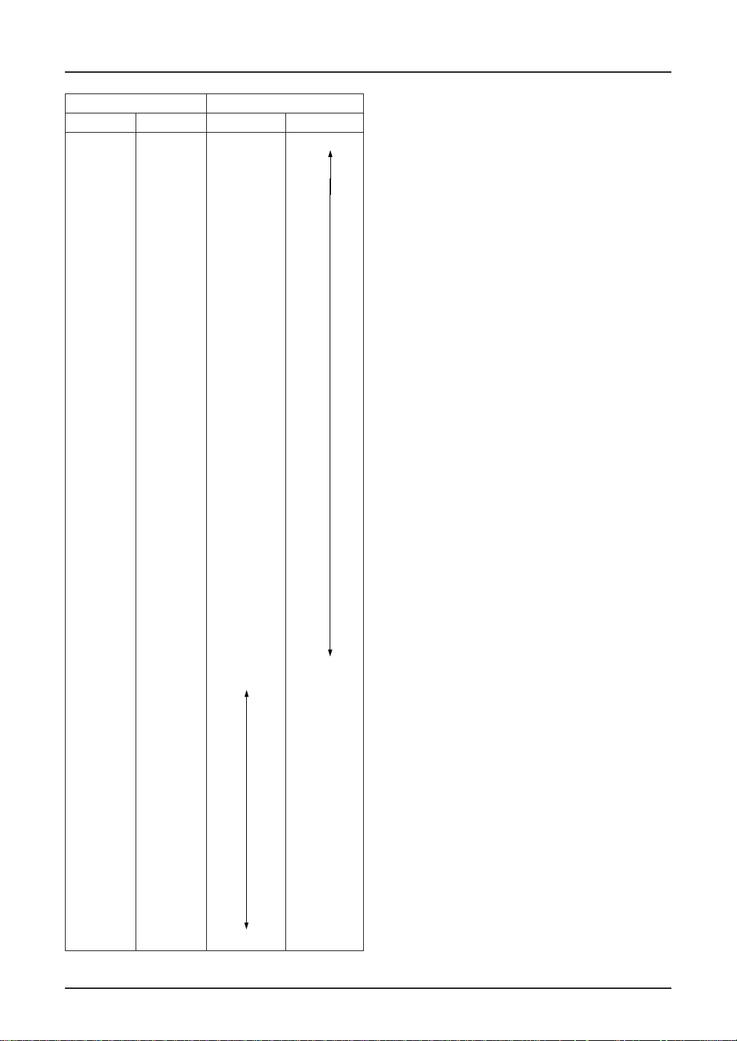
SED1220
PAD COORDINATES
No. Name X Y
109 SEG31 119 1204
110 SEG32 19
111 SEG33 –81
112 SEG34 –181
113 SEG35 –281
114 SEG36 –381
115 SEG37 –481
116 SEG38 –581
117 SEG39 –681
118 SEG40 –781
119 SEG41 –881
120 SEG42 –981
121 SEG43 –1081
122 SEG44 –1181
123 SEG45 –1281
124 SEG46 –1381
125 SEG47 –1481
126 SEG48 –1581
127 SEG49 –1681
128 SEG50 –1781
129 SEG51 –1881
130 SEG52 –1981
131 SEG53 –2081
132 SEG54 –2181
133 SEG55 –2281
134 SEG56 –2381
135 SEG57 –2481
136 SEG58 –2581
137 SEG59 –2681
138 SEG60 –2781
139 SEGS4 –2881
140 SEGS5 –2981
141 COM24 –3081
142 COM23 –3181
143 COM22 –3281
144 NC –3500
145 NC –3600
146 NC –3700 1204
147 COM21 –3670 1000
148 COM20 900
149 COM19 800
150 COM18 700
151 COM17 600
152 COM16 500
153 COM15 400
154 COM14 300
155 COM13 200
156 COM12 100
157 COM11 0
158 COM10 –100
159 COM9 –200
160 COMS2 –300
161 SEGSA –433
162 SEGSB –533
163 SEGSC –633
164 SEGSD –733
165 SEGSE –3670 –833
2–6 EPSON
Page 9
SED1220
<SED1222D**>
PAD COORDINATES
No. Name X Y
1 A0 –3312 –1228
2 WR –3180
3 CS –3048
4 D7 –2916
5 D6 –2784
6 D5 –2652
7 D4 –2520
8 D3 –2388
9 D2 –2256
10 D1 –2124
11 D0 –1992 –1228
12 V
13 V
14 V5 –1226
15 V
16 V
17 V2 –386
18 V
19 V
20 VR 454
21 V
22 CAP2– 1014
23 CAP2+ 1294
24 CAP1– 1574
25 CAP1+ 1854
26 V
27 VDD 2414 –1204
28 CK 2692 –1228
29 VS1 2836
30 P/S 2980
31 I/F 3124
32 RES 3268 –1228
33 V
34 (FSA) 3603 –796
35 (FSB) –696
36 (FSC) –596
37 (FS0) –496
38 (FS1) –396
39 (FS2) –296
40 (FS3) 3603 –196
41 V
42 COMSA 63
43 COMS1 199
44 COM1 323
45 COM2 447
46 COM3 571
47 COM4 695
48 COM5 819
49 COM6 943
50 COM7 1067
51 COM8 3694 1191
52 SEG1 3472 1228
53 SEG2 3348 1228
54 SEG3 3224 1228
DD –1786 –1204
SS –1506
4 –946
3 –666
1 –106
0 174
OUT 734
SS 2134
DD 3694 –919
DD 3694 –73
Unit: µm
PAD COORDINATES
No. Name X Y
55 SEG4 3100 1228
56 SEG5 2976
57 SEG6 2852
58 SEG7 2728
59 SEG8 2604
60 SEG9 2480
61 SEG10 2356
62 SEG11 2232
63 SEG12 2108
64 SEG13 1984
65 SEG14 1860
66 SEG15 1736
67 SEG16 1612
68 SEG17 1488
69 SEG18 1364
70 SEG19 1240
71 SEG20 1116
72 SEG21 992
73 SEG22 868
74 SEG23 744
75 SEG24 620
76 SEG25 496
77 SEG26 372
78 SEG27 248
79 SEG28 124
80 SEG29 0
81 SEG30 –124
82 SEG31 –248
83 SEG32 –372
84 SEG33 –496
85 SEG34 –620
86 SEG35 –744
87 SEG36 –868
88 SEG37 –992
89 SEG38 –1116
90 SEG39 –1240
91 SEG40 –1364
92 SEG41 –1488
93 SEG42 –1612
94 SEG43 –1736
95 SEG44 –1860
96 SEG45 –1984
97 SEG46 –2108
98 SEG47 –2232
99 SEG48 –2356
100 SEG49 –2480
101 SEG50 –2604
102 SEG51 –2728
103 SEG52 –2852
104 SEG53 –2976
105 SEG54 –3100
106 SEG55 –3224
107 SEG56 –3348
108 SEG57 –3472 1228
SED1220
(FS*) : Being fuse adjusting pins, maintain them on floating state.
CK pins : Should be V
DD when not being used.
EPSON 2–7
Page 10
SED1220
PAD COORDINATES
No. Name X Y
109 SEG58 –3694 1191
110 SEG59 1067
111 SEG60 943
112 COM16 819
113 COM15 695
114 COM14 571
115 COM13 447
116 COM12 323
117 COM11 119
118 COM10 75
119 COM9 –49
120 COMS2 –173
121 SEGSA –335
122 SEGSB –459
123 SEGSC –583
124 SEGSD –707
125 SEGSE –3694 –831
2–8 EPSON
Page 11

SED1220
<SED122AD**>
PAD COORDINATES
No. Name X Y
1 NC –3700 –1204
2 NC –3600
3 NC –3500
4 A0 –3252
5 WR –3132
6 CS –3012
7 D7 –2892
8 D6 –2772
9 D5 –2652
10 D4 –2532
11 D3 –2412
12 D2 –2292
13 D1 –2172
14 D0 –2052
15 V
16 V
17 VSS –1556
18 V
19 V
20 V5 –1176
21 V
22 V
23 V3 –716
24 V
25 V
26 V
27 V1 –156
28 V
29 V
30 V0 224
31 V
32 V
33 VOUT 684
34 V
35 CAP2– 964
36 CAP2– 1064
37 CAP2+ 1244
38 CAP2+ 1344
39 CAP1– 1524
40 CAP1– 1624
41 CAP1+ 1804
42 CAP1+ 1904
43 V
44 V
45 VDD 2364
46 V
47 CK 2693
48 VS1 2821
49 P/S 2949
50 I/F 3077
51 RES 3205
52 NC 3500
53 NC 3600
54 NC 3700 –1204
DD –1836
DD –1736
SS –1456
5 –1276
4 –996
4 –896
3 –616
2 –436
2 –336
1 –56
0 124
R 404
R 504
OUT 784
SS 2084
SS 2184
DD 2464
Unit: µm
PAD COORDINATES
No. Name X Y
55 VDD 3670 –910
56 (FSA) 3603 –796
57 (FSB) –696
58 (FSC) –596
59 (FS0) –496
60 (FS1) –396
61 (FS2) –296
62 (FS3) 3603 –196
63 V
DD 3670 –82
64 COMSA 61
65 COMS1 203
66 COM1 303
67 COM2 403
68 COM3 503
69 COM4 603
70 COM5 703
71 COM6 803
72 COM7 903
73 COM8 3670 1003
74 NC 3700 1204
75 NC 3600
76 NC 3500
77 SEGS1 3319
78 SEGS2 3219
79 SEG1 3119
80 SEG2 3019
81 SEG3 2919
82 SEG4 2819
83 SEG5 2719
84 SEG6 2619
85 SEG7 2519
86 SEG8 2419
87 SEG9 2319
88 SEG10 2219
89 SEG11 2119
90 SEG12 2019
91 SEG13 1919
92 SEG14 1819
93 SEG15 1719
94 SEG16 1619
95 SEG17 1519
96 SEG18 1419
97 SEG19 1319
98 SEG20 1219
99 SEG21 1119
100 SEG22 1019
101 SEG23 919
102 SEG24 819
103 SEG25 719
104 SEG26 619
105 SEG27 519
106 SEG28 419
107 SEG29 319
108 SEG30 219 1204
SED1220
(FS*) : This is a fuse adjusting terminal. Set it to floating state.
CK pins : Set it to V
DD when not used.
EPSON 2–9
Page 12

SED1220
PAD COORDINATES
No. Name X Y
109 SEG31 119 1204
110 SEG32 19
111 SEG33 –81
112 SEG34 –181
113 SEG35 –281
114 SEG36 –381
115 SEG37 –481
116 SEG38 –581
117 SEG39 –681
118 SEG40 –781
119 SEG41 –881
120 SEG42 –981
121 SEG43 –1081
122 SEG44 –1181
123 SEG45 –1281
124 SEG46 –1381
125 SEG47 –1481
126 SEG48 –1581
127 SEG49 –1681
128 SEG50 –1781
129 SEG51 –1881
130 SEG52 –1981
131 SEG53 –2081
132 SEG54 –2181
133 SEG55 –2281
134 SEG56 –2381
135 SEG57 –2481
136 SEG58 –2581
137 SEG59 –2681
138 SEG60 –2781
139 SEGS4 –2881
140 SEGS5 –2981
141 NC –3081
142 NC –3181
143 NC –3281
144 NC –3500
145 NC –3600
146 NC –3700 1204
147 COM16 –3670 1000
148 COM15 900
149 COM14 800
150 COM13 700
151 COM12 600
152 COM11 500
153 COM10 400
154 COM9 300
155 COMS2 200
156 SEGSA 67
157 SEGSB –33
158 SEGSC –133
159 SEGSD –233
160 SEGSE –333
161 SEGSF –433
162 SEGSG –533
163 SEGSH –633
164 SEGSI –733
165 SEGSJ –3670 –833
2–10 EPSON
Page 13
SED1220
DESCRIPTION OF PINS
Power Pins
Pin name I/O Description Q’ty
V
DD
V
SS
V
0, V1
V
2, V3 The voltage determined in the liquid crystal cell is resistance-
V
4, V5 divided or impedance-converted by operational amplifier, and the
VS1 O Power supply voltage output pin for oscillating circuit, and DC/DC 1
Power supply
Power supply
Power supply
Connected to logic supply. Common with MPU power terminal VCC.1
0V power terminal connected to system ground. 1
Multi-level power supply for liquid crystal drive. 6
resultant voltage is applied.
The potential is determined on the basis of V
DD and the following
equation must be respected.
V
DD = V0 ≥ V1 ≥ V2 ≥ V3 ≥ V4 ≥ V5
VDD ≥ VSS ≥ V5 ≥ VOUT
When the built-in power supply is ON, the following voltages are
given to pins V1 to V4 by built-in power circuit:
V
1 = 1/5 V5 (1/4 V5)
V
2 = 2/5 V5 (2/4 V5)
V
3 = 3/5 V5 (3/4 V5)
V
4 = 4/5 V5 (4/4 V5)
voltage ratings in ( ) are for optinal choices.
source. Don’t connect this pin to an external load.
SED1220
LCD Power Circuit Pins
Pin name I/O Description Q’ty
CAP1+ O Capacitor positive side connecting pin for boosting. 1
This pin connects the capacitor with pin CAP1–.
CAP1– O Capacitor negative side connecting pin for boosting. 1
This pin connects a capacitor with pin CAP+.
CAP2+ O Capacitor positive side connecting pin for boosting. 1
This pin connects a capacitor with pin CAP2–.
CAP2– O Capacitor negative side connecting pin for boosting. 1
This pin connects a capacitor with pin CAP2+.
V
OUT O Output pin for boosting. This pin connects a smoothing capacitor 1
with V
DD pin.
V
R I Voltage regulating pin. This pin gives a voltage between VDD and 1
V
5 by resistance-division of voltage.
EPSON 2–11
Page 14
SED1220
Pins for System Bus Connection
Pin name I/O Description Q’ty
D7 (SI) I 8-bit input data bus. These pins are connected to a 8-bit or 16-bit 8
D6 (SCL) standard MPU data bus.
D5 ~ D0 When P/S = “Low”, the D7 and D6 pins are operated as a serial data
input and a serial clock input respectively.
P/S RES I/F D7 D6 D5 D4 D3-D0 CS A0 WR
“L” — — SI SCL — — OPEN CS A0 —
“H” “H” “H” D7 D6 D5 D4 D3-D0 CS A0 E
“H” “L” “H” D7 D6 D5 D4 D3-D0 CS A0 WR
“H” “L” “L” D7 D6 D5 D4 OPEN CS A0 WR
RES: Indicates the active potential.
OPEN:Though “OPEN” is available, fixing the potential is
recommended for noise-withstnading characteristical reason.
—: Indicates that it can be set at either “H” or “L”, but fixing the
potential is required.
A0 I Usually, this pin connects the least significant bit of the MPU address 1
bus and identifies a data command.
0 : Indicates that D0 to D7 are a command.
1 : Indicates that D0 to D7 are display data.
RES I In case of a 68 series MPU, initialization can be performed by 1
changing RES
initialization can be performed by changing
A reset operation is performed by edge sensing of the RES signal.
An interface type for the 68/80 series MPU is selected by input level
after initialization.
“L” : 68 series MPU interface
“H” : 80 series MPU interface
CS I Chip select signal. Usually, this pin inputs the signal obtained by 1
decoding an address bus signal. At the “Low” level, this pin is
enabled.
WR I <When connecting an 80 series MPU>
Active “Low”. This pin connects the WR signal of the 80 series 1
(E) MPU. The signal on the data bus is fetched at the rise of the WR
signal.
<When connecting a 68 series MPU>
Active “High”. This pin becomes an enable clock input of the 68
series MPU.
P/S I This pin switches between serial data input and parallel data input. 1
. In case of an 80 series MPU,
.
P/S
“High” CS A0 D0~D7 –
“Low” CS A0 SI SCL
IF I Interface data length select pin for parallel data input. 1
“High”: 8-bit parallel input
“Low”: 4-bit parallel input
When P/S = “Low”, connect this pin to V
CK I External input terminal
It must be fixed to “High” when the internal oscillation circuit is used. 1
2–12 EPSON
Chip Select Data/Command
Data Serial Clock
DD or VSS.
Page 15

SED1220
Liquid Crystal Drive Circuit Signals
Dynamic drive terminal (SED1220D**/1221D**/122AD**)
Pin name I/O Description Q’ty
COM1~
COM24
COMS1,
CMOS2 CMOS1, CMOS2: Common output for symbol display
SEG1~
SEG60
SEGS1, 2
4, 5 SEGS1, SEGS2: Segment output for signal output
Dynamic drive terminal (SED1222D**)
Pin name I/O Description Q’ty
COM1~
COM16
COMS1,
CMOS2 CMOS1, CMOS2: Common output for symbol display
SEG1~
SEG60
O Common signal output pin (for characters) 24
O
O Segment signal output pin (for characters) 60
O
O Common signal output pin (for characters) 16
O
O Segment signal output pin (for characters) 60
Common signal output pin (except for characters)
Segment signal output pin (except for characters)
Common signal output pin (except for characters)
2
SED1220
4
2
Static drive terminal
Pin name I/O Description Q’ty
COMSA O Common signal output pin (for icon) 1
SEGSA, B
C, D, E O
F, G, H, I, J
Note: For the electrode of liquid crystal display panel to be connected to the static drive terminal, we recommend
you to use a pattern in which it is separated from the electrode connected to the dynamic drive terminal.
When this pattern is too close to the other electrode, both the liquid crystal display and electrode will be
deteriorated.
Segment signal output pin (for icon) 5 to
SEGSF, G, H, I, J (only SED122A) 10
EPSON 2–13
Page 16
SED1220
FUNCTIONAL DESCRIPTION
MPU Interface
Selection of interface type
In the SED1220 Series, data transfer is performed through a 8-bit or 4-bit data bus or a serial data input (SI). By selecting
“High” or “Low” as P/S pin polarity, a parallel data input or a serial data input can be selected as shown in Table 1.
Table 1
P/S Type CS A0 WR SI SCL D0~D7
“High” Parallel Input CS A0 WR — — D0~D7
“Low” Serial Input CS A0 H, L SI SCL —
Parallel Input
In the SED1220 Series, when parallel input is selected (P/S = “High”), it can be directly connected to the 80 series MPU
bus or 68 series MPU bus, as shown in Table 2, if either “High” or “Low” is selected as RES pin polarity after a reset input,
because the RES pin has an MPU select function.
Selection between 8 bits and 4 bits is performed by command.
Table 2
RES input polarity Type A0 WR CS D0~D7
↓ active 68 series A0 E CS D0~D7
↓
active 80 series A0 WR CS D0~D7
Interface with 4-bit MPU interface
When data transfer is performed by 4-bit interface (IF = 0), an 8-bit command, data and address are divided into two parts.
CS
WR
D7 to D4 Upper (D7 to D4) Lower (D3 to D0)
Note: When performing writing in succession, reverse a time exceeding the system cycle time (t
perform writing.
Serial interface (P/S = “Low”)
The serial interface consists of a 8-bit shift register and a 3-bit counter and acceptance of an SI input or SCL input is enabled
in the ship selected status (CS = “Low”).
When no chip is selected, the shift register and counter are reset to the initial status.
Serial data is input in the order of D7, D6 .... D0 from the serial data input pin (SI) at the rise of Serial Clock (SCL).
At the rising edge of the 8th serial clock, the serial data is converted into 8-bit parallel data and this data is processed.
The A0 input is used to identify whether the serial data input (SI) is display data or a command. That is, when A0 = “High”,
it is regarded as display data. When A0 = “Low”, it is regarded as a command.
The A0 input is read in and identified at the rise of the 8 x n-th clock of Serial Clock (SCL) after chip selection.
Fig. 1 shows a timing chart of the serial interface.
Regarding the SCL signal, special care must be exercised about terminal reflection and external noise due to a wire length.
We recommend the user to perform an operation check with a real machine.
We also recommend the user to periodically refresh the write status of each command to prevent a malfunction due to noise.
cyc) and then
2–14 EPSON
Page 17

CS
SED1220
SI
SCL 1
D7 D6 D5 D4 D3 D2 D1 D0 D7
23456789
A0
Fig. 1
Identification of data bus signals
The SED1220 series identifies data bus signals, as shown in Table 3, by combinations of A0 and WR (E).
Table 3
Common 68 series 80 series
A0 E WR
Function
1 1 0 Writing to RAM and symbol register
0 1 0 Writing to internal register (command)
Chip select
The SED1220 series has a chip select pin (CS). Only when CS = “Low”, MPU interfacing is enabled.
In any status other than Chip Select, D0 to D7 and A0, WR, SI and SCL inputs are invalidated. When a serial input interface
is selected, the shift register and counter are reset.
However, the Reset signal is input regardless of the CS status.
Power Circuit
This is a low-power-consumption power circuit that generates a voltage required for liquid crystal drive.
The power circuit consists of a boosting circuit, voltage regulating circuit and voltage follower.
SED1220
The power circuit incorporated in the SED1220 Series is set for a small-scale liquid crystal panel, so that its display quality
may be greatly deteriorated if it is used for a liquid crystal panel with a large display capacity.
In this case, an external power supply must be used.
A power circuit function can be selected by power control command. With this, an external power supply and a part of
the internal power supply can be used together.
Amplifying Voltage regulat- Voltage External Amplifying
circuit ing circuit follower voltage input system pin
●● ●● ●● — Per specification
Note 1
Note 2
Note 3
× ●● ●● V
××●● V
×××
OUT OPEN
5 = VOUT OPEN
V1, V2, V3, V4, V5
OPEN
Note 1: When the boosting circuit is turned off, make boosting system pins (CAP1+, CAP1-, CAP2+, CAP2-) open
and give a liquid crystal drive voltage to the V
OUT pin from the outside.
Note 2: When the voltage regulating circuit is not used with the boosting circuit OFF, make the boosting system pins
Note 3: When all the internal power supplies are turned off, supply liquid crystal drive voltages V
open, connect between the V
5 pin and VOUT pin, and give a liquid crystal drive voltage from the outside.
1, V2, V3, V4 and
V5 from the outside, and make the CAP1+, CAP1-, CAP2+, CAP2- and VOUT pins open.
EPSON 2–15
Page 18
SED1220
Voltage Tripler Circuit
If capacitors are connected between CAP+1 – CAP–1
and CAP2+,CAP2– and VSS VOUT, VDD– VSS potential
is negatively tripled and generated at VOUT terminal.
When the voltage is boosted double, open CAP2+ and
connect CAP2– to V
OUT terminal.
At this time, the oscillating circuit must be operating
since the amplifying circuit utilize the signal from the
oscillation output.
VDD=0V
=
V
S1
-2V
V
OUT=VS1
=-4V
DD
=0V
V
=
V
S1
-2V
V
OUT
=
=3VS1 -6V
Potential relationship of amplified voltage
Voltage regulating circuit
Amplified voltage generated at V
OUT outputs liquid crystal drive voltage V5 through the voltage regulation circuit.V5
voltage can be obtained from the expression 1 below by adjusting the resistors Ra and Rb within the range of
V5<VOUT.calculated by the following formula:
V0
Rb
VDD
REG with the
5
V
R
V5= (1 +
Ra
b
) • V
Where, VREG is the constant power supply within IC.
REG is maintained constantly at VREG 2.0V.
V
Voltage regulation of V
..............................
REG
5 output is done by connecting to
1
•
=
•
a variable register between VR, VDD and V5. It is
recommended to combine fixed registers R1 and R3 with
variable resistor R2 for fine adjustment of V
5 voltage.
[Sample setting on R1, R2 and R3]
• R1 + R2 + R3 = 1.2 M ohm (decided from the current
05 passed between VDD – V5. Where, I05≤5 µA
value I
is supposed).
• Variable voltage range provided by R2 is from –4V to
–6V (to be decided considering charecteristics of the
liquid crystal).
• Since V
REG = 2.0V, if the electronic volume register is
set at (0, 0, 0, 0, 0), followings are derived from above
1
conditions and expression
:
VR
R2
VREG
+
-
R3
R1
Ra
R1 = 400KΩ
R2 = 200KΩ
R3 = 600KΩ
The voltage regulation circuit outputs V
temperature gradient of approximately –0.04%/°C.
R terminal has high input impedance, anti-noise
Since V
measures must be considered including use of shortened
wiring distance and shield wire.
2–16 EPSON
Page 19

●Voltage Regulation Circuit Using Electronic Volume
Function
SED1220
The electronic volume function allows to control the
liquid crystal drive voltage V
5 with the commands and
thus to adjust density of the liquid crystal display.
Liquid crystal drive voltage V
5 can have one of 32
When using the electronic volume function, you need to
turn the voltage regulation circuit on using the supply
control command.
voltage values if 5-bit data is set to the electronic volume
register.
[Sample constants setting when electronic volume function is used]
V
0
R
a
V
R
V
= (1 +
5
R
Ra
b
) • V
EV
...............................
Where VEV = VREG – α
REG / 150
α = V
2
V
REG
SED1220
V
DD
n
α
. . . .
α
V
EV
0
+
-
R
b
V
5
No. Electronic volume register a V5
0 (0, 0, 0, 0, 0) 0 Large
1 (0, 0, 0, 0, 1) 1α •
2 (0, 0, 0, 1, 0) 2α •
3 (0, 0, 0, 1, 1) 3α •
•• ••
•• ••
30 (1, 1, 1, 1, 0) (n-1)α •
31 (1, 1, 1, 1, 1) nα Small
When the electronic volume function is not used, select (0, 0, 0, 0, 0) for the electronic volume register.
EPSON 2–17
Page 20

SED1220
Liquid crystal voltage generating circuit
V
5 potential is resistive divided within IC to produce V1,
2, V3 and V4 potentials required for driving the liquid
V
crystal. V1, V2, V3 and V4 potentials are then subject to
impedance conversion and provided to the liquid crystal
drive circuit.
The liquid crystal drive voltage is fixed to 1/5 (1/4) bias.
The liquid crystal power terminals V
1 – V5 must be
externally connected with the voltage regulating capacitor
C2.
When a built-in supply is used
When voltage is doubled
V
C1
SS
CAP1+
CAP1–
When voltage is tripled
V
SS
CAP1+
C1
CAP1–
CAP2+
CAP2–
V
OUT
V
5
V
R
V
DD
, V
1
V
V
2
V
3
V
4
V
5
V
S1
0
SED1220D
✽✽
R2
C2
C2
C2
C2
C2
C2
R3
R1
CAP2–
OUT
V
V
5
V
R
V
DD
, V
V
1
V
2
V
3
V
4
V
5
V
S1
0
SED1220D
C1
C1C1
R3
R2
R1
✽✽
C2
C2
C2
C2
C2
C1
Reference setting values: C1: 0.1 - 4.7 µF We recommend the user to set the optimum values to capacitors C1
C2: 0.1 µF and C2 according to the panel size watching the liquid crystal display
and drive waveforms.
2–18 EPSON
Page 21

SED1220
Example 2: When using the built-in power source
(VC, VF, P) = (1, 1, 0)
C2
C2
C2
C2
C2
C2
External
power
source
SED1220D
V
SS
CAP1+
CAP1-
CAP2+
CAP2V
OUT
R
3
V
R
2
R
1
5
V
R
VDD, V
V
1
V
2
V
3
V
4
V
5
V
S1
0
**
Example 3: When using the built-in power source
(VC, VF, P) = (0, 1, 0)
C2
C2
C2
C2
C2
C2
External
power
source
V
SS
CAP1+
CAP1CAP2+
CAP2-
V
OUT
V
5
V
R
VDD, V
V
1
V
2
V
3
V
4
V
5
V
S1
SED1220D
V
0
SS
**
Reference setting values: C1: 0.47 - 4.7 µF We suggest you to determine the most appropriate capacitance values,
C2: 0.1 - 4.7 µF fitting to the panel size, for respective capacitors C1 and C2 in consideration
of the liquid crystal display and drive waveforms.
SED1220
When a built-in supply is used
V
SS
CAP1+
CAP1–
OUT
V
V
5
V
R
V
DD
, V
DD
SED1220D
V
1
V
External
power
supply
2
V
3
V
4
V
5
✽✽
EPSON 2–19
Page 22

SED1220
Low Power Consumption Mode
SED1220 is provided with standby mode and sleep mode
for saving power consumption during standby period.
● Standby Mode
Switching between on and off of the standby mode is
done using the power save command.
In the standby mode, only static icon is displayed.
1. Liquid crystal display output
COM1 ~ COM24, COMS1, COMS2 : V
SEG1 ~ SEG60, SEGS1, 2, 4, 5 : V
SEGSA, B, C, D, E, F, G, H, I, J, COMSA: Can be
turned on by static drives.
Use the static icon RAM for controlling the static
icon display done with SEGSA, B, C, D, E, COMSA.
2. DD RAM, CG RAM and symbol register
Written information is saved as it is irrespective of on
or off of the stand-by mode.
3. Operation mode is retained the same as it was prior
to execution of the standby mode.
The internal circuit for the dynamic display output is
stopped.
4. Oscillating circuit
The oscillation circuit for the static display must be
remained on.
●Sleep Mode
To enter the sleep mode, turning off the power circuit and
oscillation circuit using the commands, and then execute
power save command. This mode helps to save power
consumption by reducing current to almost resting current level.
1. Liquid crystal display output
COM1 ~ COM24, COMS1, COMS2 : V
SEG1 ~ SEG60, SEGS1, 2, 4, 5 : V
SEGSA, B, C, D, E, F, G, H, I, J, COMSA: Clear all
the data of the static icon registers to “0”.
2. DD RAM, CG RAM and symbol register
Written information is saved at it is irrespective of on
or off the sleep mode.
3. Operation mode mode is retained the same at it was
prior to execution of the sleep mode.
All internal circuits are stopped.
4. Power circuit and oscillation circuit
Turn off the built-in supply circuit and oscillation
circuit using the power save command and supply
control command.
DD level
DD level
DD level
DD level
Reset Circuit
Upon activation of the RES input, this LSI will be
initialized.
●Initial State
1. Display on/off control
C = 0 : Cursor off
B = 0 : Blink off
D = 0 : Display off
2. Power save
O = 0 : Oscillation off
PS = 0 : Power save off
3. Supply control
VC = 0 : Voltage regulation circuit off
VF = 0 :Voltage follower off
P = 0 : Amplifying circuit off
4. System setting
N2, N1 = 0 : 2 lines
S = 0 : Left-hand shift
CG = 0 : “CGRAM” blank
5. Electronic volume control
Address :28H
Data : (0, 0, 0, 0, 0)
6. Static icon
Address :20H
Data : (0, 0, 0, 0, 0)
Address :21H
Data : (0, 0, 0, 0, 0)
Address :22H
Data : (0, 0, 0, 0, 0)
Address :23H
Data : (0, 0, 0, 0, 0)
As explained in the Section “MPU interface”, the RES
terminal connects to the reset terminal of the MPU and
initialization is being effected together with the MPU.
However, when the bus, port, etc. of the MPU maintains
high-impedance for a certain duration of time after
resetting, make the resetting input to the SED1220 after
the inputs to the SED1220 have become definite.
As the resetting signal, like explained in the Section “DC
characteristics”, active level pulses of minimum 10us or
more should be used. Normal operation status can be
obtained after 1us from the edge of the RES signal.
By making the RES terminal active, respective registers
can be cleared and the aforesaid setting state can be
obtained.
If initialization is not effected by the RES terminal when
the supply voltage is applied, it may go into a state where
cancellation is unworkable.
In case the built-in liquid crystal power circuit will not be
used, it becomes necessary that the RES input be active
when the external liquid crystal power is being applied.
2–20 EPSON
Page 23

COMMAND
Table 4 lists the commands. SED1220 identifies the data
bus signal using different combinations of A0 and WR
(E). High speed command interpretation and execution
are possible since only the internal timing is used.
• Command Overview
Command type Command name A0 WR
Display control Cusor Home 0 0
instruction Display ON/OFF Control 0 0
Power control Power Save 0 0
Power Control 0 0
System set System set 0 0
Address control Address Set 0 0
instruction
Data input Data Write 1 0
instruction
Instruction execution duration of dependents on the
internal process time of SED1220, therefore it is necessary to provide a duration larger than the system cycle
CYC) between execution of two successive in-
time (t
struction.
• Description of Commands
(1) Cursor Home
This command presets the address counter to 30H
and moves the cursor, when it is present, to the first
digit of the first line.
A0 WR D7 D6 D5 D4 D3 D2 D1 D0
000001
(2) Display ON/OFF Control
This command performs on or off of display and
cursor setting.
Note: Symbols driven by COMSA and SEGSA – E
must be controlled through the static icon
RAM.
A0 WR D7 D6 D5 D4 D3 D2 D1 D0
000011CB*D
D = 0 : Display off
1 : Display on
B = 0 : Cursor blink off
1 : Cursor blink on
Blink displays characters in black and white,
alternately. The alternating display will be repeated
with approx. 1 second interval.
C = 0 : Display of cursor
1 : Does not display
Following table shows relationship between B and
C registers and the cursor.
****
∗ : Don't Care
C B Cursor display
0 0 Non-display
0 1 Non-display
1 0 Underbar cursor
1 1 Alternate display of display
characters in black and white.
The cursor position indicates the
position of address
(C, B) (0, 0) (1, 0) (1, 1)
f Blink
The cursor position indicates the position of address
counter.
Therefore, whenever moving the cursor, change
the address counter value using the RAM address
set command or the auto increment done by writing
the RAM data.
ISelective flashing symbol display is possible by
selecting (C, B) = (1, 0) and thus locating the
address counter to the position of the symbol register
through selecting (since the symbol is corresponding
to the character at each 5 dots).
(3) Power Save
This command is used to controlling the oscillation
circuit and setting or resetting the sleep mode.
A0 WR D7 D6 D5 D4 D3 D2 D1 D0
000100
PS = 0 : Power save off (reset)
1 : Power save on (set)
O = 0 : Oscillating circuit off (stop of
oscillation)
1 : Oscillating circuit on (oscilla
tion)
(4) Supply Control
This command is used for controlling operation of
the built-in power circuit.
A0 WR D7 D6 D5 D4 D3 D2 D1 D0
0001010VCVFP
P = 0 : Amplifying circuit off
1 : Amplifying circuit on
Note: The oscillation circuit must be turned on
for the amplitying circuit to be active.
**
∗ : Don't Care
SED1220
SED1220
OPS
EPSON 2–21
Page 24

SED1220
VF =0 : Voltage follower off
1 : Voltage follower on
VC = 0 : Voltage regulation circuit off
1 : Voltage regulation circuit on
(5) System Set
This command is used for selecting display line,
common shift direction and use/non-use of CR
RAM.
When power on or resetting is done, execute this
command first.
A0 WR D7 D6 D5 D4 D3 D2 D1 D0
000110
N1 N2
∗ : Don't Care
N2, N1 = 0, 0 : 2lines
N2, N1 = 0, 1 : 3lines
S = 0 : COM left shift
= 1 : COM right shift
CG = 0 : Use CG RAM
1 : Does not use RAM
SCG
RAM Map
(6) RAM Address Set
This command sets addresses to write data into the
DD RAM, CG RAM and symbol register in the
address counter.
When the cursor is displayed, the cursor is displayed at the display position corresponding to the
DD RAM address set by this command.
A0 WR D7 D6 D5 D4 D3 D2 D1 D0
001
1
The settable address length is ADDRESS = 00H to
ADDRESS
7FH.
2
Before writing data into the RAM, set the data
write address by this command. Next, when data is
written in succession, the address is automatically
incremented.
0 0 H
1 0 H
2 0 H
3 0 H
4 0 H
5 0 H
6 0 H
7 0 H
0123456789ABCDEF
C G R A M (0 0 H)
C G R A M (0 2 H)
SI
DDRAM line 1
DDRAM line 2
DDRAM line 3
Symbol register
Symbol register
SI
EV
Test
–
For signals
For symbol register
:Static icon register
:Electronic volume register
:Test register (Do not use)
EV Test
For signals
:Unused
:Output from SEGS1 to SEGS2, SEGS4, SEGS5
:Output from COMS1 to COMS2.
C G R A M (0 1 H)
C G R A M (0 3 H)
Unused
"
"
"
"
2–22 EPSON
Page 25

SED1220
(7) Data Write
A0 WR D7 D6 D5 D4 D3 D2 D1 D0
10
1
This command writes data the DD RAM, CG RAM
DATA
or symbol register.
2
This command automatically increases the address
counter by +1, thus enabling continuous writing of
data.
<Example of Data Writing>
Following figures illustrates an example of con-
tinuous writing of one line data to DD RAM.
NO
RAM Address Set
Data Writing
One Line Completed?
YES
Note: When executing
instructions in
succession, reserve a
time exceeding t
and execute the next
instruction.
SED1220
CYC
EPSON 2–23
Page 26

SED1220
Table 4 SED1220 Series Command List
Command
(1) Cursor Home 0 0 0 001****Moves the cursor to the home position.
(2) Display ON/OFF 0 0 0 0 1 1 C B * D Sets cursor ON/OFF (C), cursor blink ON//OFF (B),
Control and display ON/OFF (D).
(3) Power Save 0 0 0 100**0PSSets power save ON/OFF (PS) and oscillating circuit
(4) Power Control 0 0 0 1010VCVFPSets voltage regulating circuit ON/OFF and boosting
(5) System Set 0 0 0 1 1 0 N2 N1 S CG Sets the use or non-use of CG RAM and shifting
(6) RAM Address Set 0 0 1 ADDRESS Sets the DD RAM, CG RAM or symbol register
(7) RAM Write 1 0 DATA Writes data into the DD RAM, CG RAM or symbol
(8) NOP 0 0 0 0000000Non-operation command
(9) Test Mode 0 0 0 000****Command for IC chip test. Don’t use this command.
A0WRD7 D6 D5 D4 D3 D2 D1 D0
Code
Function
C = 1 (cursor ON) 0 (cursor OFF), B = 1 (blink ON)
0 (blink OFF), D = 1 (display ON)
D = 0 (display OFF)
ON/OFF (0).
PS = 1 (power save ON) 0 (power save OFF),
0 = 1 (oscillating circuit ON) 0 (oscillating circuit
OFF)
circuit ON/OFF (P).
VC = 1 (voltage regulating circuit ON) 0 (voltage
regulating circuit OFF) VF = 1 (voltage follower
ON) 0 (voltage follower OFF), P = 1 (boosting
circuit ON) 0 (boosting circuit OFF)
direction of display line (N1, N2) and COM
CG = 1 (use of CG RAM), 0 = (Does not use
CG RAM),
M2, N1 = 0, 0 (2 lines) 0, 1 (3 lines).
S = 0 (left shift), 1 (right shift).
address.
register address.
CHARACTER GENERATOR
Character Generator ROM (CG ROM)
Character Generator ROM (CG ROM)
SED1220 cntains the character generator ROM (CG
ROM) consisted of up to 256 types of characters.
Character size is 5 × 8 dots.
Tables 5 though 7 show the SED1220** character code.
Concerning the 4 characters from 00H through 03H, the
2–24 EPSON
system command selects on which of CG ROM and CG
RAM they are to be used.
SED1220 CG ROM is mask ROM and compatible with
customized ROM. Contact us for its use in your system.
Product name of modified CG ROM is defined as below:
(Example) S E D 1 2 2 0 D
0 B
↑
Digit for CG ROM
pattern change
Page 27

SED1220
SED1220DA
0
1
2
3
4
5
6
*
Lower 4 Bit of Code
0123456789ABCDEF
SED1220
7
8
Higher 4 Bit of Cord
9
A
B
C
D
E
F
EPSON 2–25
Page 28
SED1220
SED1220DB
0
1
2
3
4
5
6
*
Lower 4 Bit of Code
0123456789ABCDEF
7
8
Higher 4 Bit of Cord
9
A
B
C
D
E
F
2–26 EPSON
Page 29
SED1220
SED1220DG
0
1
2
3
4
5
6
*
Lower 4 Bit of Code
0123456789ABCDEF
SED1220
7
8
Higher 4 Bit of Cord
9
A
B
C
D
E
F
EPSON 2–27
Page 30

SED1220
Character Generator RAM (CG ROM)
CGRAM contained in SED1220 enables user programming of character patterns for display signals with higher degrees
of freedom.
When using CGRAM, select it using the system command.
Capacity of CGRAM is 160 bits and accepts registration of any 4 5 × 8 dots patterns.
Following shows relationship between the CGRAM characters, CGRAM addresses and character code.
00H
02H
01H
03H
RAM addressCharacter code
00H~07H
10H~17H
08H~0FH
18H~1FH
CGRAM data (character pattern)
D7 D0 SEG
0
***
1
***
2
***
3
***
4
***
5
***
6
***
7
***
8
***
9
***
A
***
B
***
C
***
D
***
E
***
F
***
0
1
1
1
1
0
0
0
1
0
0
0
0
1
1
1
0
0
0
0
0
0
0
0
1
1
1
1
0
0
0
0
0
0
1
0
0
0
1
0
0
1
1
1
0
1
1
1
0
1
1
1
1
1
1
1
0
0
0
0
0
0
0
0
1
0
0
1
1
1
0
0
0
0
0
0
0
1
0
0
Signal displayCharacter display
SEGS
12 45
Unused Character data
1: Display
0: Non-display
It is possible to set a 5 × 8 character size in this system. In this case, use the
is inverted when a under-bar cursor is used.
7H/*FH RAM. Note that the *7H/*FH data
*
2–28 EPSON
Page 31
SED1220
Symbol Register
SED1220 contains the symbol register which enable individual symbol setting for displaying on the screen.
Capacity of the symbol register is 120 bits and is capable of displaying up to 120 symbols.
Following shows relationship between the symbol register display patterns, RAM addresses and written data.
13121
SEGS4 5SEG562345 60
COMS1
COMS2
13
15660234
61 65 116 120
··· ···
SEG1SEG1 2
RAM address
60H~6BH
70H~7BH
D7 D0
0
***
1
***
··
B
***
0
***
1
***
··
B
***
Symbol Bits
1
2
6
7
·· ··
56
57
61
62
66
67
116
117
···5
3
8
58
63
68
118
4
9
59
64
69
119
5
10
60
65
70
120
Note: When the symbol is 1.5 times or more than the character, it is recommended to drive it using both COMS1
and COMS2.
SED1220
EPSON 2–29
Page 32

SED1220
Static Icon Ram
SED1220 contains the static icon RAM for displaying
the static icons in addition to the dynamic icons.
Capacity of static icon RAM is 10 bits (SED1220/1221/
1222) or 20 bit (SED122A) and is capable of displaying
< SEGSA, B, C, D, E >
Function
Display
On/Off
Blink
On/Off
< SEGSF, G, H, I, J >
Function
Display
On/Off
Blink
On/Off
RAM address
20H
21H
RAM address
22H
23H
D7 D0 S E G S A B C D E
***
***
D7 D0 S E G S F G H I J
***
***
up to 5 icons (SED1220/1221/1222) or 10 icons
(SED122A).
Following shows relationship between the static icons
functions, static icon RAM addresses and written data.
Static icon data
00111
1000
Static icon data
00111
1000
1
1
Display
f BLINK
Display
f BLINK
*: Blank
1: Display or blink on
0: Display or blink off
f
BLINK: 1–2 Hz
Electronic Volume RAM (register)
SED1220 contains the electronic volume function for
controlling the liquid crystal drive voltage V5 and density
of liquid crystal display. The electronic volume function
enables to select one of 32 voltage status of the liquid
Function RAM address
Electronic
volume data
28H
29H
* : Blank
Note : Do not use the address “29H”. It is for testing
α = V
D7 D0
REG
/150
crystal drive voltage V5 by writting 5-bit data to the
electronic volume RAM.
Following shows relationship between RAM addresses
set by the electronic volume and written data.
Electronic volume data
***
***
***
***
***
***
*****
·· ··
00000
Condi-
tion
0
110000
200000
·· ··
2910111
3001111
3111111
EV
V
REG
–0
V
REG
–α
V
REG
–2α
V
REG
–29α
V
REG
–30α
V
REG
–31α
V
For testing
2–30 EPSON
Page 33

ABSOLUTE MAXIMUM RATINGS
Item Symbol Standard value Unit
Power supply voltage (1) VSS –6.0~+0.3 V
Power supply voltage (2) V
Power supply voltage (3) V1, V2, V3, V4 V5~+0.3 V
Input voltage VIN VSS–0.3~+0.3 V
Output voltage V
Operating temperature Topr –30~+85 °C
Storage temperature
TCP
Bare chip –65~+125
5, Vout –7.0~+0.3 V
O VSS–0.3~+0.3 V
T
str
–55~+100
°C
SED1220
SED1220
(VCC) V
(GND) V
DD
SS
Notes: 1. All the voltage values are based on VDD = 0 V.
2. For voltages of V1, V2, V3 and V4, keep the condition of VDD ≥ V1 ≥ V2 ≥ V3 ≥ V4 ≥ V5 and VDD ≥ VSS
≥ V5 ≥ VOUT at all times.
3. If the LSI is used exceeding the absolute maximum ratings, it may lead to permanent destruction.
In ordinary operation, it is desirable to use the LSI in the condition of electrical characteristics. If the
LSI is used out of this condition, it may cause a malfunction of the LSI and have a bad effect on the
reliability of the LSI.
V
DD
V
5
EPSON 2–31
Page 34

SED1220
DC CHARACTERISTICS
VDD = 0 V, VSS = –3.6 V to –2.4 V, Ta = –30 to 85°C unless otherwise specified.
Item Symbol Condition min typ max Unit Applicable pin
Power Operatable V
supply Data retain –3.6 –2.0 *1
voltage (1) voltage
Power Operatable V
supply Operatable V
voltage (2) Operatable V3, V4 V5 0.4×V5 VV3, V4
High-level input voltage VIHC 0.2×VSS VDD V*3
Low-level input voltage V
Input leakage current I
LC driver ON resistance R
Static current consumption I
Dynamic current IDD Display state V5 = –6 V without load 80
consumption Standby state Oscillation ON, Power 20
Input pin capacity C
SS –3.6 –3.0 –2.4 V VSS
5 –7.0 –4.0 V V5 *2
1, V2 0.6
ILC VSS 0.8
LI VIN = VDD or VSS –1.0 1.0
ON Ta=25
DDQ 0.1 5.0
°
CV5=–7.0V 20 40 KΩCOM,SEG
∆
V=0.1V *4
×
V5 VDD VV1, V2
×
VSS V*3
µ
µ
µ
µ
OFF, VSS = –3V
without load
Sleep state Oscillation OFF, Power 5
µ
OFF, VSS = –3.0V
Access state f
IN Ta=25
cyc=200KHz, 500
V
SS = –3.0V
°
C f=1MHz 5.0 8.0 pF *3
µ
A*3
AVDD
AVDD *5
AVDD
AVDD
AVDD *6
Frame frequency f
External clock frequency f
FR Ta=25
ck Display of 2 lines 23.4 KHz *10 *11
f
ck Display of 3 lines 33.8 KHz *10 *11
°
C VSS=–3.0V 70 100 130 Hz *10
Reset time tR 1.0
Reset pulse width t
Reset start time t
RW 10
RES 50 ns *8
Dynamic system
Input voltage VS1 –2.3 –2.1 –1.9 V *9
Amplified voltage V
OUT When voltage is tripled –6.9 –6.3 –5.7 V VOUT
output voltage
Voltage follower V
5 –7.0 –4.0 V
operating voltage
Reference voltage V
Built-in power supply
*1: A wide operating voltage range is guaranteed but an
abrupt voltage variation in the access status of the
MPU is not guaranteed.
REG Ta = 25
°
C –2.06 –2.0 –1.94 V
*4: This is a resistance value when a voltage of 0.1 V is
applied between output pin SEGn, SEGSn, COMn or
COMSn, and each power pin (V
is specified in the range of operating voltage (2).
ON = 0.1 V / ∆I
*2: When the voltage is Tripled, care must be paid to
supply the voltage V
SS so that operating voltage of
VOUT and V5 may not be exceeded.
R
(∆I: Current flowing when 0.1 V is
applied between the power and output)
*3: D0 ~ D5, D6 (SCL), D7 (SI), A0, RES, CS WR (E),
P/S, IF
µ
s*7
µ
s*8
1, V2, V3 or V4). It
2–32 EPSON
Page 35
SED1220
*5: Character “ ” display. This is applicable to the
case where no access is made from the MPU and the
built-in power circuit and oscillating circuit are in
operation.
*6: Current consumption when data is always written by
cyc.
f
The current consumption in the access state is almost
proportional to the access frequency (f
When no access is made, only I
tR (reset time) indicates the internal circuit reset
*7:
cyc).
DD (I) occurs.
completion time from the edge of the RES signal.
Accordingly, the SED1220 usually enters the operating state after
tR.
*8: Specifies the minimum pulse width of the RES
signal. It is reset when a signal having the pulse
width greater than tRW is entered.
V
Power Supply
DD
V
SS
V
DD
RES
V
SS
All signal timings are based on 20% and 80% of V
–2.4 V
t
RES
t
RW
SS
signals.
t
R
*9: When operating the boosting circuit, the power
supply V
SS must be used within the input voltage
range.
*10:The f
OSC frequency of the oscillator circuit for
internal circuit drive may differ from the fBST boosting clock on some models. The following provides
the relationship between the f
OSC frequency, fBST
boosting clock, and fFR frame frequency.
f
OSC = (No. of digits) × (1/Duty) × fFR
fBST = (1/2) × (1/No. of digits) × fOSC
*11:When performing the operations using an external
clock, not taking advantage of the built-in oscillation
circuit, input the waveforms indicated below.
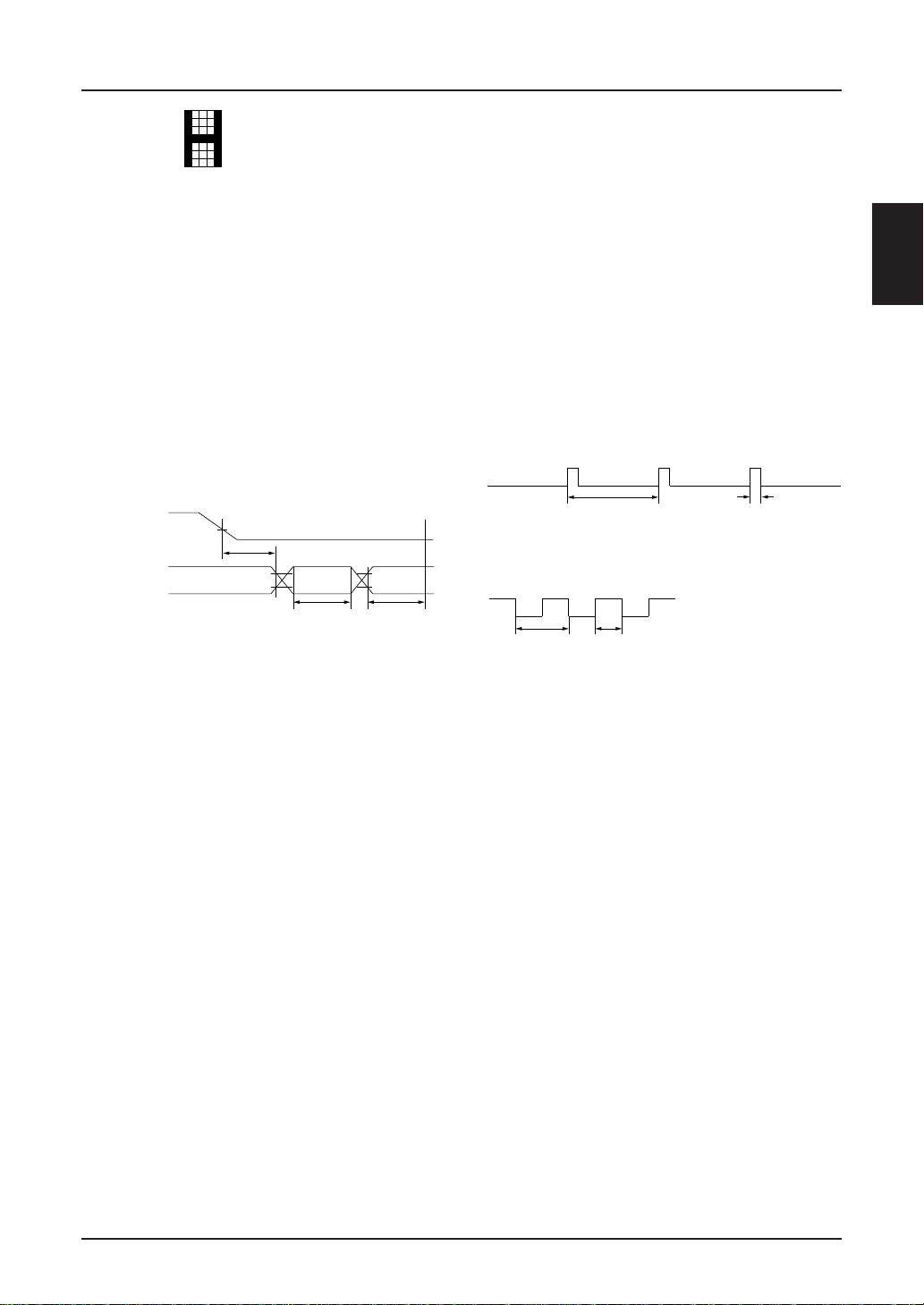
Meanwhile, while using an external clock but when
clock inputs are not being made, fix it to “H”.
(Normal High)
<Incase the external clock = fosc>
• Duty = (t
h/tosc) × 100 = 20 ~ 30%
• fosc = 1/tosc
t
osc
t
h
<Incase the external clock = 4 × fosc>
• Duty = (t
h/tosc) × 100 = 50%
• fosc = 1/tosc
t
t
osc
h
SED1220
EPSON 2–33
Page 36

SED1220
TIMING CHARACTERISTICS
(1) MPU Bus Write Timing (80 series)
A0
t
AC8
CS
t
AW8
WR
D0 to D7
Item Signal Symbol
Address hold time A0, CS t
Address setup time t
CS setup time t
System cycle time WR t
Write “L” pulse width (WR) t
Write “H” pulse width (WR) t
Data setup time D0 ~ D7 t
Data hold time t
AH8
t
t
t
CCL
t
DS8
cyc8
t
DH8
t
CCH
[Ta = –30 to 85°C, VSS = –3.6 V to –2.4 V]
Measuring
condition
AH8 Every timing is specified 30 – ns
AW8 on the basis of 20% and 60 – ns
AC8 80% of VSS.0–ns
CYC8 650 – ns
CCL 150 – ns
CCH 450 – ns
DS8 100 – ns
DH8 50 – ns
Min. Max. Unit
[Ta = –30 to 85°C, VSS = –3.3 V to –2.7 V]
Item Signal Symbol
Address hold time A0, CS t
Address setup time t
CS setup time t
System cycle time WR t
Write “L” pulse width (WR) t
Write “H” pulse width (WR) t
Data setup time D0 ~ D7 t
Data hold time t
AH8 Every timing is specified 10 – ns
AW8 on the basis of 20% and 60 – ns
AC8 80% of VSS.0–ns
CYC8 500 – ns
CCL 100 – ns
CCH 350 – ns
DS8 100 – ns
DH8 20 – ns
Measuring
condition
Min. Max. Unit
*1: For the rise and fall of an input signal (tr and tf), set a value not exceeding 25ns (excluding RES input).
t
r
V
SS
× 0.8 [V]
V
SS
× 0.2 [V]
*2:
tCCL is specified based on an overlap period of CS and WR “L” levels.
t
f
2–34 EPSON
Page 37
(2) MPU Bus Write Timing (68 series)
A0
CS
t
EWL
E
D0 to D7
Item Signal Symbol
Address setup time A0, CS t
Address hold time t
CS setup time t
System cycle time WR t
Enable “L” pulse width (WR)
Enable “H” pulse width (WR)
Data setup time D0 ~ D7 t
Data hold time t
SED1220
t
t
AH6
SED1220
DH6
t
AC6
t
EWH
t
DS6
t
AW6
t
CYC6
[Ta = –30 to 85°C, VSS = –3.6 V to –2.4 V]
Measuring
condition
AW6 Every timing is specified 60 – ns
AH6 on the basis of 20% and 30 – ns
AC6 80% of VSS.0–ns
CYC6 650 – ns
Min. Max. Unit
tEWL 150 – ns
tEWH 450 – ns
DS6 100 – ns
DH6 50 – ns
[Ta = –30 to 85°C, VSS = –3.3 V to –2.7 V]
Item Signal Symbol
Address setup time A0, CS t
Address hold time t
CS setup time t
System cycle time WR t
Enable “L” pulse width (WR)
Enable “H” pulse width (WR)
Data setup time D0 ~ D7 t
Data hold time t
AW6 Every timing is specified 60 – ns
AH6 on the basis of 20% and 10 – ns
AC6 80% of VSS.0–ns
CYC6 500 – ns
tEWL 100 – ns
tEWH 350 – ns
DS6 100 – ns
DH6 20 – ns
Measuring
condition
Min. Max. Unit
*1: For the rise and fall of an input signal (tr and tf), set a value not exceeding 25ns (excluding RES input).
t
r
V
SS
× 0.8 [V]
SS
× 0.2 [V]
V
EWH is specified based on an overlap period of CS “L” and E “H” levels.
*2: t
t
f
EPSON 2–35
Page 38

SED1220
(3) Serial Interface
CS
A0
SCL
t
CSS
t
SAS
t
SLW
t
SCYC
t
SAH
t
SHW
t
CSH
t
SDS
t
SDH
SI
[Ta = –30 to 85°C, VSS = –3.6 V to –2.4 V]
Item Signal Symbol
System clock cycle SCL t
SCL “H” pulse width t
SCL “L” pulse width t
Address setup time A0 t
Address hold time t
Data setup time SI t
Data hold time t
CS-SCL time CS t
SCYC Every timing is specified 1000 ns
SHW on the basis of 20% and 300 ns
SLW 80% of VSS. 300 ns
SAS 50 ns
SAH 300 ns
SDS 50 ns
SDH 50 ns
CSS 150 ns
t
CSH 700 ns
Measuring
condition
Min. Max. Unit
*1: For the rise and fall of an input signal (tr and tf), set a value not exceeding 25ns (excluding RES input).
t
r
V
SS
SS
V
× 0.8 [V]
× 0.2 [V]
t
f
2–36 EPSON
Page 39
SED1220
MPU INTERFACE (REFERENCE EXAMPLES)
The SED1220 Series can be connected to the 80 series MPU and 68 series MPU. When an serial interface is used, the
SED1220 Series can be operated by less signal lines.
80 Series MPU
V
MPU
CC
A0
A1 to A7
IORQ
Decoder
A0
CS
V
DD
SED1220
P/S
SED1220
68 Series MPU
MPU
Serial Interface
GND
V
CC
GND
D0 to D7
WR
RES
A0
A1 to A7
VMA
D0 to D7
RES
D0 to D7
WR
IF
RES
SS
V
RESET
V
A0
DD
P/S
Decoder
CS
SED1220
D0 to D7
E
E
IF
RES
SS
V
RESET
MPU
V
CC
GND
Port4
Port3
Port1
Port2
RES
RESET
V
A0
DD
P/S
CS
SED1220
SI
SCL
IF
RES
SS
V
V
SS
or GND
EPSON 2–37
Page 40

SED1220
INTERFACE TO LCD CELLS (REFERENCE)
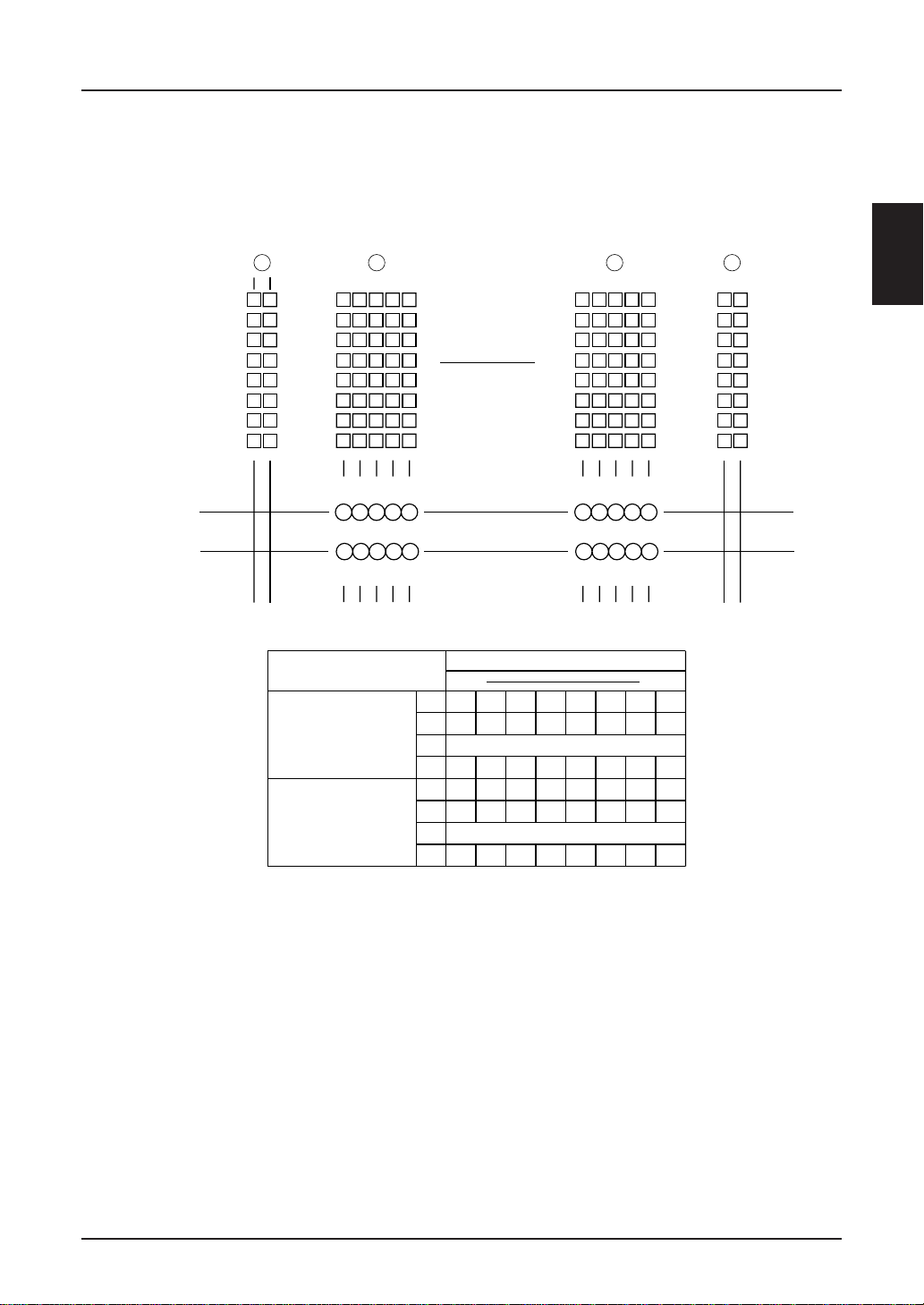
12 columns by 3 lines, 5 × 8-dot matrix segments and symbols
SED 1220
COMSA
SEGSA
. .
SEGSE
COMS1
COMS2
COM1
COM9
10
11
12
13
14
15
16
LCD panel
static icon
signal signal
2
3
4
5
6
7
8
. . . . . . . . . . . . . . . . .
112
symbol
COM17
18
19
20
21
22
23
24
SEGS1
SEGS2
SEG1
2
3
4
5
. .
SEG60
SEGS4
SEGS5
2–38 EPSON
character
Page 41
12 columns by 2 lines, 5 × 8-dot matrix segments and symbols
SED1220
SED 1221
COMSA
SEGSA
. .
SEGSE
COMS1
COMS2
COM1
COM9
10
11
12
13
14
15
16
SEGS1
SEGS2
SEG1
. .
SEG60
SEGS4
SEGS5
LCD panel
static icon
. . . . . . . . . . . . . . .
112
SED1220
symbol
signal signal
2
3
4
5
6
7
8
character
2
3
4
5
EPSON 2–39
Page 42

SED1220
12 columns by 2 lines, 5 × 8-dot matrix segments and symbols
SED 1222
COMSA
SEGSA
. .
SEGSE
COMS1
COMS2
COM1
COM9
10
11
12
13
14
15
16
LCD panel
static icon
2
3
4
5
6
7
8
• • • • • • • • • • • • • •
1
symbol
12
SEG1
. .
SEG60
character
2
3
4
5
2–40 EPSON
Page 43

12 columns by 2 lines, 5 × 8-dot matrix segments and symbols
SED1220
SED 122A
COMSA
SEGSA
• •
SEGSJ
COMS1
COMS2
COM1
COM9
10
11
12
13
14
15
16
LCD Panel
Static icon
• • • • • • • • • • • • • •
1
12
SED1220
Symbol
Signal Signal
2
3
4
5
6
7
8
Character
SEGS1
SEGS2
SEG1
• •
SEG60
SEGS4
SEGS5
2
3
4
5
EPSON 2–41
Page 44
SED1220
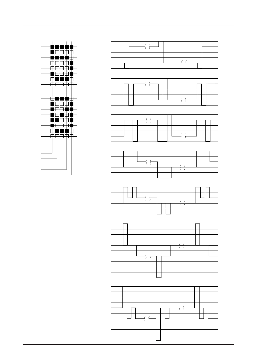
LIQUID CRYSTAL DRIVE WAVEFORMS (B WAVEFORMS)
COM 1
COM 2
COM 3
COM 4
COM 5
COM 6
COM 7
COM 8
COM 9
COM 10
COM 11
COM 12
COM 13
COM 14
COM 15
COM 16
SEG 1
SEG 2
SEG 3
SEG 4
SEG 5
COM 1
COM 2
COM 3
SEG 1
V
DD
V
1
V
2
V
3
V
4
V
5
V
DD
V
1
V
2
V
3
V
4
V
5
V
DD
V
1
V
2
V
3
V
4
V
5
V
DD
V
1
V
2
V
3
V
4
V
5
SEG 2
COMO -SEG 1
COMO -SEG 2
V
DD
V
1
V
2
V
3
V
4
V
5
V
5
V
4
V
3
V
2
V
1
V
DD
-V
1
-V
2
-V
3
-V
4
-V
5
V
5
V
4
V
3
V
2
V
1
V
DD
-V
1
-V
2
-V
3
-V
4
-V
5
2–42 EPSON
Page 45
Instruction Setup Example
(Reference Only)
SED1220
(1) Initial setup
VDD-VSS power ON
Power regulation
Input of reset signal
Command status
• Static display control: Off
• Display on/off control: Off
• Power save: Off
• Power control: Off
• System setup: Off
• Electronic volume (0, 0, 0, 0, 0)
• Static icon (0, 0, 0, 0, 0)
• Others are undefined.
Waiting for 10 sec or more
Command input:
(Asterisk indicates any command sequence.)
(1)
NOP command
(2)
System setup command
()
Electronic volume register setup
• Address: 28H
• Data: ( , , , , )
Power save command
()
• PS: Off (Power save)
• O: On (Oscillation)
Power control commands
(5)
• P, VF, VC: On
RAM address setup
(6)
Data writing
(7)
1)
1)
(2) Display mode
Input of RAM address setup command
Input of RAM (data) write command
End of initialization
SED1220
Display of written data
Waiting for 20msec or more
Command input
(8) Display on/off control command
• D: On (Display)
Data input
(9) Static icon control
• Address: 20H
• Data: ( , , , , )
• Address: 21H
• Data: ( , , , , )
3)
End of initialization
2)
3)
Notes 1) Commands (6) and (7) initialize the RAM. The display contents must first be set. The non-display area
must satisfy the following conditions (for RAM clear).
• DDRAM: Write the 20H data (character code).
• CGRAM: Write the 00H data (null data).
• Symbol register: Write the 00H data (null data).
As the RAM data is unstable during reset signal input (after power-on), null data must be written. If not,
unexpected display may result.
2) Since it is specified based on rise characteristics of the booster, power control and voltage follower
circuits, time to be set differs depending on external capacity. Be sure to set it after the external capacity
is confirmed.
3) A display of the dynamic drive series is turned on when the on command is input and the static icon is
turned on using the static icon control command.
To turn both on at the same time when the display is turned on, execute display on/off command and
static icon control within 1 frame period.
EPSON 2–43
Page 46

SED1220
(3-1) Selecting the Standby mode (3-2) Releasing the Standby mode
End of initialization
Normal operation
(Power Save is released and
oscillator circuit is turned ON.)
(1) Input of display on/off control command
• D: Off (Display)
(2) Input of power save command
• PS: On (Power save)
• O: On (Oscillation)
(3) Input of power control command
• P, VF, VC: Off
Standby status
Only static icon displayed
(4-1) Selecting the Sleep mode
Standby mode
(1) Input of power save command
• PS: Off (Power save)
• O: On (Oscillation)
(2) Input of power control command
• P, VF, VC: On
Waiting for 20msec or more
(3) Input of display on/off control command
• D: Off (Display)
Return to normal operation (initial status).
(4-2) Releasing the Sleep mode
2)
End of initialization
Normal operation
(Power Save is released and
oscillator circuit is turned ON.)
(1) Input of display on/off control command
• D: Off (Display)
(2) Static icon control
• Address: 20H
• Data: (0, 0, 0, 0, 0)
• Address: 21H
• Data: (0, 0, 0, 0, 0)
(3) Input of power save command
• PS: On (Power save)
• O: Off (Oscillation)
(4) Input of power control command
• P, VF, VC: Off
Enter the Sleep mode.
Sleep mode
(1) Input of power save command
• PS: Off (Power save)
• O: On (Oscillation)
(2) Input of power control command
• P, VF, VC: On
Waiting for 20msec or more
(3) Input of display on/off control command
• D: Off (Display)
(4) Static icon control
• Address: 20H
• Data: ( , , , , )
• Address: 21H
• Data: ( , , , , )
Return to normal operation (initial status).
3)
2)
3)
2–44 EPSON
Page 47

Instruction Setup Example of SED1220 series
(1) Initial setup
(2) display ON “EPSON”
(3) Display ON the Icon
(4) Standby Mode sequence
(5) Releasing the Standby Mode sequence
<Diagram of SED1220Txx and LCD Panel>
Static Icon
SED1220
SED1220
COMSA
COMS1
COM1
VDDRES
COM8
SEGS1
I/F
P/S
. . . . . . . . . . . . . . . . . . . . . . . . . . . . ... .. ..
SEGS2
SEG1
SED1220D
AB
SEG60
SEGS4
SEGS5
COM24
CHIP:REVERSE
VS1CK
VDDVSSCAP1+
CAP1-
CAP2+
CAP2-
VOUT
VRV0V1V2V3V4V5VSSVDDD0D1D2D3D4D5D6D7CSWRA0
80series MPU
DDVSS
V
COM9
COMS2
SEGSA
SEGSE
EPSON 2–45
Page 48

SED1220
(1) Initial setup
(1.1) VDD–VSS Power ON
(1.2) Power regulation
(1.3) Input of RESET signal
(1.4) Command Status
• Display ON/OFF :OFF
• Power save :OFF
• Power control :OFF
• System reset :OFF
• Electronic Volume :(0, 0, 0, 0, 0)
• Static display control :OFF
• Others are undefined.
(1.5) Waiting for 10µ sec or more
(1.6) Command Input: ((*) indicates any command sequence.)
(a) System Setup command: CGRAM→Not use, 3lines, COM Left shift
A0 WR D7 D6 D5 D4 D3 D2 D1 D0
0001100100
(*) Electronic volume resister setup: Data→(0, 0, 0, 0, 0, 0)
A0 WR D7 D6 D5 D4 D3 D2 D1 D0
0010101000
1000000000
(*) Power save command: PS→0, 0→1
A0 WR D7 D6 D5 D4 D3 D2 D1 D0
0001000/10/110
(d) Power Control command: P, VF, VC→1
A0 WR D7 D6 D5 D4 D3 D2 D1 D0
0001010111
(e) (f) RAM address setup, Data writing
• RAM address setup: Set address is 30H
A0 WR D7 D6 D5 D4 D3 D2 D1 D0
0010110000
2–46 EPSON
Page 49

• Data writing: All data→20H (for 1 Line)
A0 WR D7 D6 D5 D4 D3 D2 D1 D0
1000100000
1000100000
1000100000
1000100000
1000100000
1000100000
1000100000
1000100000
1000100000
1000100000
1000100000
1000100000
1000100000
• RAM address setup: Set address is 40H
A0 WR D7 D6 D5 D4 D3 D2 D1 D0
0011000000
SED1220
SED1220
• Data writing: All data→20H (for 2 line)
A0 WR D7 D6 D5 D4 D3 D2 D1 D0
1000100000
1000100000
1000100000
1000100000
1000100000
1000100000
1000100000
1000100000
1000100000
1000100000
1000100000
1000100000
1000100000
• RAM address setup: Set address is 50H
A0 WR D7 D6 D5 D4 D3 D2 D1 D0
0011010000
EPSON 2–47
Page 50
SED1220
• Data writing: All data →20H (for 3 Line)
A0 WR D7 D6 D5 D4 D3 D2 D1 D0
1000100000
1000100000
1000100000
1000100000
1000100000
1000100000
1000100000
1000100000
1000100000
1000100000
1000100000
1000100000
1000100000
• End of Initialization
(2) Display ON “EPSON”
(2.1) RAM address setup command: 30H
A0 WR D7 D6 D5 D4 D3 D2 D1 D0
0010110000
(2.2) Data writing command: Writing “EPSON”
A0 WR D7 D6 D5 D4 D3 D2 D1 D0
1001000101E: 45H
1001010000P: 50H
1001010011S: 53H
1001001111O: 4FH
1001001110N: 4EH
(2.3) Waiting for 20ms or more
(2.4) Display ON/OFF control command: B, C→0, D→1
A0 WR D7 D6 D5 D4 D3 D2 D1 D0
0000110001
Display ON 5×7 Dots “EPSON”
EPSON
2–48 EPSON
Page 51

(3) Display ON The Icon: Valid in Standby mode only
(3.1) Display ON/OFF command: D→OFF
A0 WR D7 D6 D5 D4 D3 D2 D1 D0
0000110000
(3.2) Static display control command: 1 ~ 2Hz Blink
A0 WR D7 D6 D5 D4 D3 D2 D1 D0
0010100000
1000010000
0010100001
1000010000
(3.3) Power save command: PS→ON, 0→ON
A0 WR D7 D6 D5 D4 D3 D2 D1 D0
0001000/10/111
(3.4) Power control commands: P, VF, VC→OFF
A0 WR D7 D6 D5 D4 D3 D2 D1 D0
0001010000
SED1220
SED1220
Display ON the Icon
(4) Releasing the Standby Mode
(4.1) Power save command: PS→0, 0→1
A0 WR D7 D6 D5 D4 D3 D2 D1 D0
0001000/10/110
(4.2) Power control commands: P, VF, VC→1
A0 WR D7 D6 D5 D4 D3 D2 D1 D0
0001010111
(4.3) Waiting for 20ms or more
(4.4) Display ON/OFF command: D→1
A0 WR D7 D6 D5 D4 D3 D2 D1 D0
0000110001
END of Releasing the Standby mode
e
EPSON 2–49
Page 52

SED1220
Option List
SED1220 provides the optional functions as described in
the following. Being adaptable to the customer’s optional
demand, contact the Business Department of our company
when installed.
o
Our product name corresponding to a customer’s
option is defined as shown below:
(Example) SED1220D
1. Specification of Character Generator ROM
(CGROM)
SED1220 integrates a character generator ROM
which can generate a maximum of 256 type characters.
The size of these characters is composed of 5 × 7 (8)
dots.
Being a mask ROM, the SED1220 CGROM is
adaptable to the character generator ROM exclusive
for the customer, too.
For our standard CGROMs, refer to the Character
Fonts Table.
2. Specification of Liquid Crystal Driver Voltage Bias
Value.
SED1220 integrates a liquid crystal diver voltage
generator circuit. Its 5-volt potential is divided into
resistance inside of IC to generate 1-V, 2-V, 3-V or
4-V potential as required for the liquid crystal driver.
Further, the 1-V, 2-V, 3-V or 4-Vpotential is converted
into impedance by a voltage follower to be supplied
to the liquid crystal driver circuit.
Either 1/5 or 1/4 bias value can be selected as
demanded by the customer.
Our standard bias value is preset to 1/5.
3. Specification of Reference Voltage of Liquid Crystal
Driver Voltage Regulation Circuit.
SED1220 integrates a voltage regulation circuit using
a booster voltage as its power supply to generate 5V
for the liquid crystal driver via the voltage regulation
circuit.
The voltage regulation circuit integrates a reference
voltage regulator V
The customer can select a specification of using
either the internal reference voltage or external V
reference voltage.
Our standard specification is preset to the internal
reference voltage.
XB
Shipping form: A (AL
pad product) or B (metal
bump product)
Option corresponding
digit
Machine type: 0 (12 digits × 3
lines) or 1 (12 digits × 2 lines)
REG.
SS
4. Power Supply to Booster Circuit
SED1220 integrates a booster circuit.
The customer can select a specification of using
either the regulator output V
S1 or VSS as the supply
voltage to the booster circuit.
Our standard specification is preset to the regulator
output V
S1.
5. External Clock Specifications
SED1220 integrates an external clock terminal and
there are two clock specifications, f and 4×f
oscillation.
Either of them can be selected on your request.
Internal External External
oscillation clock f osc.
clock 4×f osc.
Standard ●● ●● ×
Optional ●● × ●●
The standard external clock specification is set to
OSC.
f
6. Reset Signal Input Polarity Specifications
SED1220 inputs reset signal from the reset terminal
using edge detection and I/F specification 80/68
series can be selected according to this signal level.
RES input polarity can also be selected on your
request.
RES input Type
polarity Standard Optional
68 series 80 series
80 series 68 series
is set to the 68 series and to the 80 series as
the standard RES input polarities.
7. Pad Layout Specifications of COMS1 Symbol
Terminal
On SED1220, pad layout of COMS1 symbol terminal
can be changed. COMS1 pad layout can be selected
on your request.
Standard Optional
Pad No Pad Name Pad Name
65 COMS1 COM1
66 COM1 COM2
67 COM2 COM3
68 COM3 COM4
69 COM4 COM5
70 COM5 COM6
71 COM6 COM7
72 COM7 COM8
73 COM8 COMS1
2–50 EPSON
Page 53
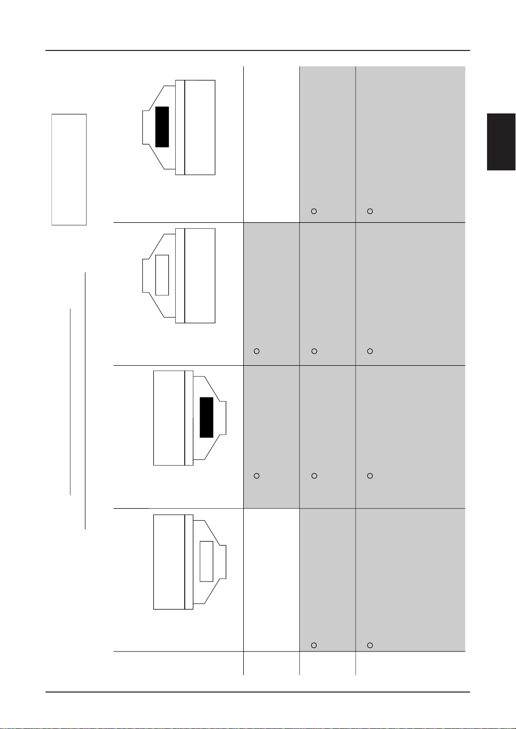
1 Case1 (Chip Front)
COM1
•
•
•
COM32
SEG60 • • • • • SEG1
(80)
(COM24, etc.)
Front
SED12XX
2 Case2 (Chip Rear)
COM1
•
•
•
COM32
SEG1 • • • • • SEG60
(80)
(COM24, etc.)
Rear
SED12XX
3 Case3 (Chip Front)
COM32
•
•
•
COM1
SEG1 • • • • • SEG60
(80)
(COM24, etc.)
Front
SED12XX
4 Case4 (Chip Rear)
COM32
•
•
•
COM1
SEG60 • • • • • SEG1
(80)
(COM24, etc.)
Rear
SED12XX
SED1240 SED1225 SED1220
SED1220/1225/1240 Example of
System Setup Depending on Mount Direction
Reference
• Unable to correspond with
commands.
• Only able to correspond with
custom fonts.
System set
• S1 = 0
• S2 = 1 (Horizontally-reversed)
System set
• S = 0
System set
• S1 = 0
• S2 = 0
System set
• CS = 0
• SS = 0
System set
• S = 1
System set
• S1 = 1 (Vertically-reversed)
• S2 = 0
System set
• CS = 1 (COM-reversed)
• SS = 0
System set
• CS = 0
• SS = 1 (SEG-reversed)
However, the input of DDRAM
address of "SED12XX" from the
first digit of the first line shall be
3FH and 3EH, in this order (as it is
reversed in the unit of character).
• Unable to correspond with
commands.
• Only able to correspond with
custom fonts.
System set
• S1 = 1 (Vertically-reversed)
• S2 = 1 (Horizontally-reversed)
System set
• CS = 1 (COM-reversed)
• SS = 1 (SEG-reversed)
However, the input of DDRAM
address of "SED12XX" from the
first digit of the first line shall be
3FH and 3EH, in this order.
SED1220
SED1220
EPSON 2–51
 Loading...