

Page 1
查询SCI7654供应商
PF754-03
SCI7654M
0A
/C
0A
DC/DC Converter
Double/Triple/Quadruple Boosting
95% Excellent Power Conversion Efficiency
Built-in Voltage Regulator
DESCRIPTION
The SCI7654 is a highly efficient, but low power-consumption DC-to-DC converter based on the advanced CMOS
technologies. It can generate an output voltage double/triple/quadruple times higher than the input (in negative
direction) if 4/3/2 external capacitors are attached.
With a built-in voltage regulator, the SCI7654 can provide a stable output by setting the DC/DC output to any voltage
via two external resistors. This is optimum to the LCD panel power supply as the stable output can have the negative
temperature gradient required for an LCD panel.
FEATURES
An input voltage can be boosted double/triple/quadruple to negative potential.
Input voltages: –2.4 to –5.5V (quadruple boosting), –2.4 to –7.3V (triple boosting), –2.4 to –11.0V (double
boosting)
Excellent vol tage conversion efficiency: 95% (Typ.)
Large output current: 20 mA (Max.) during quadruple boosting
Built-in voltage regulator (for stable voltage output)
Built-in reference voltage source for accurate regulation: –1.5 ±0.05V (CT0)
Regulator output voltage temperature gradient function: –0.04, –0.15, –0.35, –0.55%/˚C
Low current consumption: 130 µA (Typ.)
Low standby current: 5.0 µA (Max.)
Built-in oscillator circuit
5/6-time voltage boosting in negative potential by serial connection
Package: SCI7654M0A SSOP2-16pin (plastic), SCI7654C0A DIP-16pin (plastic)
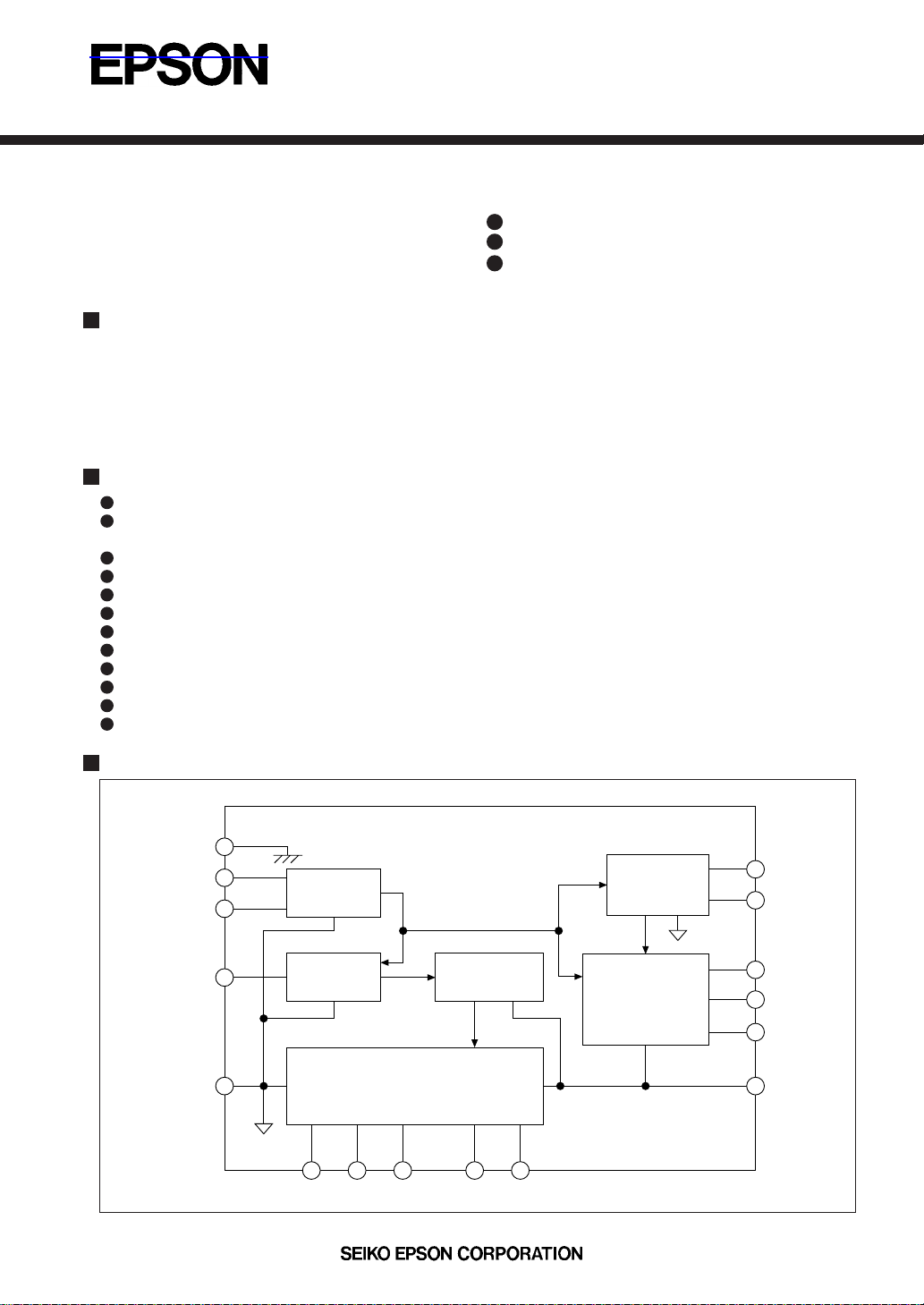
BLOCK DIAGRAM
V
DD
POFF1
POFF2
FC
V
IN
Power-Off
Control
Clock
Generator
Voltage Converter
C1P C2PC1N C3N C2N
Booster Control
Ref. Voltage
Circuit
Voltage Regulator
TC1
TC2
RV
REG
V
V
RI
V
OUT
Page 2
SCI7654M0A/C
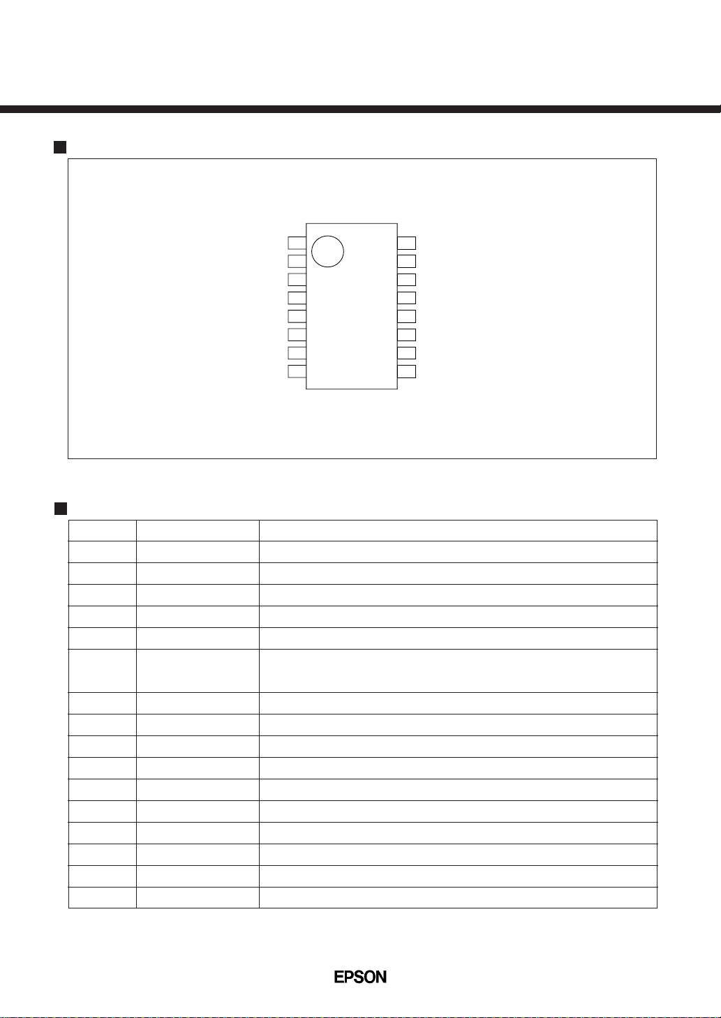
PIN CONFIGURATION
SSOP2-16pin/DIP-16pin
0A
V
V
OUT
V
REG
RV
V
DD
FC
TC1
TC2
1
RI
2
3
4
5
6
7
8
16
15
14
13
12
11
10
9
C2P
C2N
C3N
C1N
C1P
V
IN
POFF1
POFF2
PIN DESCRIPTION
Pin No. Pin Name Function
1VOUT Voltage output
2VRI Regulator input
3VREG Regulator output
4 RV Input for regulator output voltage adjustment
5VDD Input voltage pin (Positive)
6 FC Internal clock rate switch input, and clock input in serial/parallel
connection (Common input pin)
7 TC1 Input for regulator output temperature gradient setup (1)
8 TC2 Input for regulator output temperature gradient setup (2)
9 POFF2 Power-off control input (2)
10 POFF1 Power-off control input (1)
11 VIN Input voltage pin (Negative)
12 C1P Common double and quadruple boosting capacitor positive pin
13 C1N Double boosting capacitor negative pin
14 C3N Quadruple boosting capacitor negative pin
15 C2N Triple boosting capacitor negative pin
16 C2P Triple boosting capacitor positive pin
2
Page 3
SCI7654M0A/C
ABSOLUTE MAXIMUM RATINGS
Rating Symbol Min. Max. Unit Remark
Input Power Voltage VIN -26.0/N VDD +0.3 V N=Boosting time;
at VIN pin
Input Pin Voltage V
Output Pin Voltage 1 V0C1 VIN -0.3 VDD +0.3 V At C1P and C2P pins
Output Pin Voltage 2 VOC2 2 VIN -0.3 VIN +0.3 V At C1N pin
Output Pin Voltage 3 VOC3 3 VIN -0.3 2 VIN +0.3 V At C2N pin
Output Pin Voltage 4 VOC4 4 VIN -0.3 3 VIN +0.3 V At C3N pin
Regulator Input Power Voltage VRI N VIN -0.3 VDD +0.3 V N=Boosting time; at VRI pin
Regulator Input Pin Voltage VRV N VIN -0.3 VDD +0.3 V N=Boosting time; at RV pin
Output Voltage V0 N VIN -0.3 VDD +0.3 V N=Boosting time; at VOUT
Input Current IIN — 80 mA At VIN pin
Output Current IOUT — N≤4: 20 mA N=Boosting time; at VOUT
Allowable Loss Pd — 210 mW —
Operating Temperature Topr -30 85 ˚C —
Storage Temperature Tstg -55 150 ˚C —
Soldering Temperature and Time Tsol — 260•10 ˚C.S Temperature at leads
I VIN -0.3 VDD +0.3 V POFF1, POFF2
TC1, TC2, FC pins
and VREG pins
N>4: 80/N and VREG pins
0A
ELECTRICAL CHARACTERISTICS
(Unless otherwise designated: Ta=–30°V to +85°C, VDD=0V, VIN=–5.0V)
Characteristic Symbol Condition Min. Typ. Max. Unit
Input Power Voltage 1 VIN1 During quadruple boosting -5.5 — -2.4 V
Input Power Voltage 2 VIN2 During triple boosting -7.3 — -2.4 V
Input Power Voltage 3 VIN3 During double boosting -11 -2.4 V
Input Power Voltage N VINN During large-time boosting using -22/N — -2.4 V
external diodes
Boost Startup Input Power Voltage VSTA N=Boosting time, IOUT<200 A, -22/N — -2.4 V
FC=VDD
Booster Output Voltage VOUT — -22 —— V
Regulator Input Voltage VRI — -22 — -2.4 V
Regulator Output Voltage VREG IREG=0, VRI=-22V, ——-2.4 V
RRV=1MΩ
Booster Output Impedance ROUT IOUT=10mA, during quadruple — 200 300
boosting
Booster Power Conversion Peff IOUT=2 mA; during quadruple — 95 — %
Efficiency boosting;
C1, C2, C3, COUT=10 F Tantalum
Booster Operating Current IOPR1
Consumption 1 during no loading;
Booster Operating Current IOPR2
Consumption 2 during no loading;
Regulator Operating Current IOPVR VRI=-20 V, during no loading, — 10 15 A
Consumption RRV=1 M
FC=VDD, POFF1=VIN, POFF2=VDD; — 130 220 A
C1, C2, C3, COUT=10 F Tantalum
FC=VIN, POFF1=VIN, POFF2=VDD; — 520 880 A
C1, C2, C3, COUT=10 F Tantalum
3
Page 4

SCI7654M0A/C
ELECTRICAL CHARACTERISTICS (continued)
Characteristic Symbol Condition Min. Typ. Max. Unit
Static Current IQ
Input Leakage Current ILIN
Stable Output Saturation
Resistance
Stable Output Voltage Stability DVR -20V<VRI<-10V, IREG=1mA — 0.2 — %/V
Stable Output Load Variation DV0 VRI=-20V VREG=-15V — 30 50 mV
Reference Voltage VREF0 TC1 = VDD, TC2 = VDD -1.55 -1.50 -1.45 V
(Ta = 25°C) VREF1 TC1 = VDD, TC2 = VIN -1.70 -1.50 -1.30 V
Reference Voltage Temperature CT0
Coefficient (*4) CT1
(*5) CT2
Input Voltage Level
Capacitance of Booster Capacitors CMAX Capacitors ——47 µF
0A
POFF1=VIN, POFF2=VIN, FC=VDD
At POFF1, POFF2, FC, TC1, TC2 pins
RSAT 0<IREG<20mA — 10 20
(*1) RV=VDD
Ta=25˚C
(*2) VREG=-15V
Ta=25˚C
(*3) Ta=25˚C
0<IREG<20mA
VREF2 TC1 = VIN, TC2 = VDD -1.90 -1.50 -1.10 V
VREF3 TC1 = VIN, TC2 = VIN -2.15 -1.50 -0.85 V
TC1 = VDD, TC2 = VDD, SSO package
TC1 = VDD, TC2 = VIN, SSO package
TC1 = VIN, TC2 = VDD, SSO package
CT3
VIH VIN =-2.0V to -5.5V
V
TC1 = VIN, TC2 = VIN, SSO package
At POFF1, POFF2, FC, TC1, 0.2VIN —— V
TC2 pins
IL VIN =-2.0V to -5.5V
At POFF1, POFF2, FC, TC1, ——0.8VIN V
TC2 pins
C1, C2, C3
——5.0 A
——0.5 A
-0.07 -0.04 0 %/˚C
-0.25 -0.15 -0.07 %/˚C
-0.45 -0.35 -0.20 %/˚C
-0.75 -0.55 -0.30 %/˚C
(*1) R
SAT
(*2) V
R
(*3) R0=
(*4) CT =
(VREG – VOUT)
=
=
IREG
VREG
VOUT•VREG
VREG
IREG
|
VREF(50˚C)| – |VREF(0˚C)
50˚C – 0˚C
|
100
|
VREF(25˚C)
|
(*5) The reference voltage temperature coefficient of each chip product may vary depending on the used molding
materials. Perform the temperature test before use.
4
Page 5

SCI7654M0A/C
q
g
FUNCTIONAL DESCRIPTION
Clock Generator Circuit
As the SCI7654 has a built-in clock generator circuit, it requires no external source at all. The clock rate changes
depending on the FC pin signal level, and the Low Output or High Output mode can be selected. This allows
a frequency selection according to the current capacitance and load current when the booster output impedance
changes depending on the clock rate and external booster capacitance.
FC pin Mode Clock Rate Current Consumption Output Ripple
H (VDD) Low Output 4.0 kHz (Typ.) IOP VRP
L (VIN) High Output 16.0 kHz (Typ.) Approx. 4 times of IOP Approx. 1/4 time of VRI
Voltage Converter Circuit
The voltage converter receives a clock from the clock generator, and boosts the V
quadruple, triple or double. Four converter circuits are required for quadruple boosting, three converts are
required for triple boosting, and dual converters are required for double boosting.
V
DD
(0V)
V
IN
10V
(-5V)
IN input power voltage
0A
double boosting
15V
triple boosting
uadruple boostin
-10V
-15V
20V
-20V
Voltage step-up diagram (during -5V input)
Reference Voltage Circuit
The SCI7654 has a built-in reference voltage circuit for the voltage regulator. The temperature coefficient of
reference voltage can be changed using pins TC1 and TC2, and a voltage having one of four types of temperature
gradients can be output at V
Mode Min. Typ. Max. Min. Typ. Max.
TC1 TC2
REG pin for LCD driving.
Reference Voltage, V
REF (V)
Temperature Coefficient, CT (%/˚C)
CT0 H(VDD) H(VDD) -1.55 -1.5 -1.45 -0.07 -0.04 0
CT1 H L(VIN) -1.70 -1.5 -1.30 -0.25 -0.15 -0.07
CT2 L(VIN) H -1.90 -1.5 -1.10 -0.45 -0.35 -0.20
CT3 L L -2.15 -1.5 -0.85 -0.75 -0.55 -0.30
5
Page 6

SCI7654M0A/C
Voltage Regulator Circuit
The circuit receives a voltage from V
0A
RI pin, stabilizes it, and outputs at any voltage. The output is adjustable with
a ratio of R1 and R2 external divider resistors. Although the sum of divider resistors is desirable to be minimum
to prevent an interference due to external noise, 100 to 1 megohms are recommended as the current
consumption may be increased by the divider resistors.
Power Off Control
VOUT
1
2
R2R1
3
4
5
6
7
8
VRI
VREG
RV
V
FC
TC1
TC2
C2P
16
15
C2N
14
C3N
13
C1N
C1P
V
POFF1
POFF2
12
11
IN
10
9
DD
The SCI7654 has an automatic power-off function, and can turn on or off each function depending on the external
signals entered in POFF1 and POFF2 pins.
Function Status
Mode
POFF1 POFF2
Oscillator Booster Regulator Description
PS1 H(VDD) L(VIN) ON ON ON All circuits are turned ON.
PS2 L L OFF OFF (*1) OFF (*2) All circuits are turned OFF.
PS3 H H OFF ON ON Slave side (booster and regulator)
in parallel connection
Master side (for booster only)
PS4 L H ON ON OFF in parallel connection; first stage
in serial connection (*3)
*1 When the booster circuit is OFF, approximately V
IN +0.6V voltage appears at VOUT pin.
*2 When the regulator is OFF, the VREG pin is set to the high-impedance status.
*3 The mode selected depends on the line connection at the second stage of serial connection.
6
Page 7

SCI7654M0A/C
REFERENCE CIRCUIT EXAMPLE
Four-time booster circuit
This example drives the booster circuit only, boosts the V
outputs it at the VOUT pin. However, this does not have a voltage regulator and the voltage at VOUT pin may have
a ripple.
OUT
C
+
V
OUT
V
DD
+
C
IN
V
IN
IN input voltage four times in negative direction, and
1
V
OUT
2
V
RI
3
V
REG
4
RV
5
V
DD
6
FC
7
TC1
8
TC2
C2P
C2N
C3N
C1N
C1P
V
POFF1
POFF2
16
+
2
C
15
14
13
12
11
IN
C
3
C
1
+
+
10
9
0A
Four-time booster and regulator circuits
This example receives a boost output from V
OUT pin, stabilizes it via the voltage regulator circuit, and outputs
a voltage having the temperature gradient at VREG pin via the temperature gradient selector circuit.
OUT
C
+
V
REG
V
DD
C
REG
+
R
1
R
2
+
IN
C
V
IN
1
V
OUT
2
V
RI
3
V
REG
4
RV
5
DD
V
6
FC
7
TC1
8
TC2
C2P
C2N
C3N
C1N
C1P
V
POFF1
POFF2
16
+
2
C
15
14
13
12
11
IN
C
3
C
1
+
+
10
9
7
Page 8

SCI7654M0A/C
PACKAGE DIMENSIONS
0A
Plastic SSOP2-16pin
7
max
(
0.275
6.6
(
0.26
INDEX
max
±0.2
+0.007
–0.008
)
)
916
)
)
+0.008
–0.007
±0.011
±0.2
±0.3
4.4
6.2
0.244
0.173
(
(
0°
10°
0.8
(
0.031
81
±0.1
0.36
+0.004
–0.003
(
)
0.014
)
)
±0.003
1.5
0.05
0.059
(
)
0.002
(
max
1.7
max
0.066
(
0.15
(
0.006
±0.2
0.5
+0.007
–0.008
(
0.02
0.9
(
0.035
)
±0.05
+0.003
–0.002
)
)
±0.1
)
Unit : mm
(inch)
8
Page 9

Plastic DIP-16pin
16 9
18
)
+0.004
–0.003
±0.1
4.4
0.173
(
)
min
min
3
0.119
(
2.54
(
0.1
19.7
(
0.775
(
0.748
)
19
max
max
±0.1
±0.003
)
)
(
1.5
0.059
)
±0.1
0.46
+0.004
–0.003
(
0.018
)
)
±0.003
±0.1
6.3
0.248
(
)
+0.004
–0.003
±0.1
0.8
0.031
(
15°
SCI7654M0A/C
0°
7.62
(
0.3
)
+0.03
–0.01
0.25
+0.001
–0
0.01
(
0A
)
Unit : mm
(inch)
9
Page 10

NOTICE:
http://www.epson.co.jp/device/
No part of this material may be reproduced or duplicated in any form or by any means without the written permission of Seiko Epson. Seiko
Epson reserves the right to make changes to this material without notice. Seiko Epson does not assume any liability of any kind arising out of
any inaccuracies contained in this material or due to its application or use in any product or circuit and, further, there is no representation that
this material is applicable to products requiring high level reliability, such as, medical products. Moreover, no license to any intellectual
property rights is granted by implication or otherwise, and there is no representation or warranty that anything made in accordance with this
material will be free from any patent or copyright infringement of a third party. This material or portions thereof may contain technology or the
subject relating to strategic products under the control of the Foreign Exchange and Foreign Trade Law of Japan and may require an export
license from the Ministry of International Trade and Industry or other approval from another government agency.
© Seiko Epson Corporation 2000 All right reserved.
All other product names mentioned herein are trademarks and/or registered trademarks of their respective companies.
ELECTRONIC DEVICES MARKETING DIVISION
IC Marketing & Engineering Group
ED International Marketing Department I (Europe & U.S.A.)
421-8, Hino, Hino-shi, Tokyo 191-8501, JAPAN
Phone : +81-(0)42-587-5812 FAX : +81-(0)42-587-5564
ED International Marketing Department II (Asia)
421-8, Hino, Hino-shi, Tokyo 191-8501, JAPAN
Phone : +81-(0)42-587-5814 FAX : +81-(0)42-587-5110
■ EPSON Electronic Devices Website
First issue June, 1995
Printed February, 2000 in Japan T
 Loading...