

Page 1
MF302-13
IEEE1394 Controller
POWER SUPPLY IC
S1R77801F00A
S1F70000 Series
Technical Manual
Technical Manual
Page 2

NOTICE
No part of this material may be reproduced or duplicated in any from or by any means without the
written permission of Seiko Epson. Seiko Epson reserves the right to make changes to this material
without notics. Seiko Epson does not assume any liability of any kind arising out of any inaccuracies
contained in this material or due to its application or use in any product or circuit and, further, there
is no repersesnation that this material is applicable to products requiring high level reliability, such as,
medical products. Moreover, no license to any intellectual property rights is granted by implication or
otherwise, and there is no representation or warranty that anything made in accordance with this
material will be free from any patent or copyright infringement of a third party. This material or
portions thereof may contain technology or the subject relating to strategic products under the control
of the Foreign Exchange and Foreign Trade Low of Japan and may require an export licenes from the
Ministry of International Trade and Industry or other approval from another government agency.
HD44103 is a registered trademark of Hitachi, Ltd.
All other product names mentioned herein are trademarks and/or registered trademarks of their
respective companies.
©SEIKO EPSON CORPORATION 2002, All rights reserved.
Page 3
The information of the product number change
Starting April 1, 2001 the product number has been changed as listed belo w. To order , please use
the new product number. For further information, please contact Epson sales representative.
Configuration of product number
●DEVICES (Example : S1F70000D00B100)
S1 F 70000 D 00B1 00
Packing specification
Specifications
Shape (C:DIP, D:Bare chip, M:SOP, Y :SO T89)
Model number
Model name (F:Power supply ICs)
Product classification (S1:Semiconductors)
Comparison table between new and previous number
Previous number New number
SCI7660M0B S1F76600M0B0
SCI7660C0B S1F76600C0B0
SCI7662M0A S1F76620M0A0
SCI7662D0A S1F76620D0A0
SCI7661M0B S1F76610M0B0
SCI7661MBB S1F76610M2B0
SCI7661C0B S1F76610C0B0
SCI7654M0A S1F76540M0A0
SCI7654C0A S1F76540C0A0
SCI7664M0A S1F76640M0A0
SCI7664D0A S1F76640D0A0
SCI7810Y
SCI7910Y
SCI7631MLA S1F76310M1L0
SCI7631MBA S1F76310M1B0
SCI7631MKA S1F76310M1K0
SCI7631MAA S1F76310M1A0
SCI7638MHA S1F76380M1H0
SCI7638MLA S1F76380M1L0
SCI7633MBA S1F76330M1B0
SCI7110M0A S1F71100M0A0
SCI7120M0A S1F71200M0A0
SCI7120M0B S1F71200M0B0
B S1F78100Y2
*
A S1F79100Y1
*
*
*
Previous number New number
SCI7721Y
SCI7721Y
SCI7720Y
SCI7722Y
0
0
A S1F77210Y1
*
B S1F77210Y2
*
A S1F77200Y1
*
DB S1F77220Y2D0
*
*
*
0
0
0
Page 4

S1F70000 Series
Technical Manual
Page 5

Contents
Introduction .......................................................................................................................................................................... 1
Selection Guide.................................................................................................................................................................... 2
1. DC/DC Converter
S1F76600 Series
DESCRIPTION.......................................................................................................................................................... 1–1
FEATURES ............................................................................................................................................................... 1–1
APPLICATIONS ........................................................................................................................................................ 1–1
BLOCK DIAGRAM .................................................................................................................................................... 1–1
PIN ASSIGNMENTS ................................................................................................................................................. 1–1
PIN DESCRIPTIONS ................................................................................................................................................ 1–1
SPECIFICATIONS .................................................................................................................................................... 1–2
FUNCTIONAL DESCRIPTIONS ............................................................................................................................... 1–7
TYPICAL APPLICATIONS ........................................................................................................................................ 1–8
S1F76620 Series
DESCRIPTION........................................................................................................................................................ 1–10
FEATURES ............................................................................................................................................................. 1–10
BLOCK DIAGRAM .................................................................................................................................................. 1–10
PIN DESCRIPTIONS .............................................................................................................................................. 1–11
FUNCTIONAL DESCRIPTIONS ............................................................................................................................. 1–13
ELECTRICAL CHARACTERISTICS ....................................................................................................................... 1–14
EXAMPLE OF REFERENCE EXTERNAL CONNECTION ..................................................................................... 1–21
MEASUREMENT CIRCUIT..................................................................................................................................... 1–24
MECHANICAL DATA .............................................................................................................................................. 1–25
2. DC/DC Converter & Voltage Regulator
S1F76610 Series
DESCRIPTION.......................................................................................................................................................... 2–1
FEATURES ............................................................................................................................................................... 2–1
APPLICATIONS ........................................................................................................................................................ 2–1
BLOCK DIAGRAM .................................................................................................................................................... 2–1
PIN ASSIGNMENTS ................................................................................................................................................. 2–2
PIN DESCRIPTIONS ................................................................................................................................................ 2–2
SPECIFICATIONS .................................................................................................................................................... 2–3
FUNCTIONAL DESCRIPTIONS ............................................................................................................................. 2–11
TYPICAL APPLICATIONS ...................................................................................................................................... 2–12
S1F70000 Series EPSON i
Technical Manual
Page 6

Contents
S1F76540 Series
DESCRIPTION........................................................................................................................................................ 2–15
FEATURES ............................................................................................................................................................. 2–15
APPLICATIONS ...................................................................................................................................................... 2–15
BLOCK DIAGRAM .................................................................................................................................................. 2–16
PIN DESCRIPTIONS .............................................................................................................................................. 2–16
ELECTRICAL CHARACTERISTICS ....................................................................................................................... 2–19
FUNCTIONAL DESCRIPTIONS ............................................................................................................................. 2–22
CHARACTERISTICS GRAPH ................................................................................................................................ 2–29
APPLICATION CIRCUIT EXAMPLES .................................................................................................................... 2–30
S1F76640 Series
DESCRIPTION........................................................................................................................................................ 2–38
FEATURES ............................................................................................................................................................. 2–38
BLOCK DIAGRAM .................................................................................................................................................. 2–39
PIN ASSIGNMENTS ............................................................................................................................................... 2–40
PIN DESCRIPTIONS .............................................................................................................................................. 2–41
CHIP EXTERNAL SHAPE AND PAD CENTER COORDINATES .......................................................................... 2–42
FUNCTIONAL DESCRIPTIONS ............................................................................................................................. 2–43
ELECTRICAL CHARACTERISTICS ....................................................................................................................... 2–46
CHARACTERISTICS GRAPH ................................................................................................................................ 2–51
MECHANICAL DATA .............................................................................................................................................. 2–56
APPLICATION EXAMPLE ...................................................................................................................................... 2–57
3. Voltage Regulator
S1F78100Y Series
DESCRIPTION.......................................................................................................................................................... 3–1
FEATURES ............................................................................................................................................................... 3–1
BLOCK DIAGRAM .................................................................................................................................................... 3–1
PIN DESCRIPTIONS ................................................................................................................................................ 3–2
PIN ASSIGNMENTS ................................................................................................................................................. 3–2
FUNCTIONAL DESCRIPTIONS ............................................................................................................................... 3–3
LINEUP ..................................................................................................................................................................... 3–4
ABSOLUTE MAXIMUM RATINGS............................................................................................................................ 3–5
RECOMMENDED OPERATING CONDITIONS ....................................................................................................... 3–5
ELECTRICAL CHARACTERISTICS ......................................................................................................................... 3–6
EXAMPLES OF REFERENCE EXTERNAL CONNECTION .................................................................................. 3–14
MECHANICAL DATA .............................................................................................................................................. 3–14
ii EPSON S1F70000 Series
Technical Manual
Page 7

Contents
CHARACTERISTICS GRAPH ................................................................................................................................ 3–15
S1F79100Y Series
DESCRIPTION........................................................................................................................................................ 3–21
FEATURES ............................................................................................................................................................. 3–21
APPLICATIONS ...................................................................................................................................................... 3–21
LINEUP ................................................................................................................................................................... 3–21
BLOCK DIAGRAM .................................................................................................................................................. 3–21
PIN ASSIGNMENTS ............................................................................................................................................... 3–21
PIN DESCRIPTIONS .............................................................................................................................................. 3–22
SPECIFICATIONS .................................................................................................................................................. 3–22
PACKAGE MARKINGS........................................................................................................................................... 3–35
FUNCTIONAL DESCRIPTIONS ............................................................................................................................. 3–35
TYPICAL APPLICATIONS ...................................................................................................................................... 3–36
4. DC/DC Switching Regulators
S1F76300 Series
S1F76310, S1F76380 Series
DESCRIPTION ................................................................................................................................................ 4–1
FEATURES ..................................................................................................................................................... 4–1
APPLICATIONS .............................................................................................................................................. 4–1
LINEUP............................................................................................................................................................ 4–1
BLOCK DIAGRAMS ........................................................................................................................................ 4–2
PIN ASSIGNMENTS ....................................................................................................................................... 4–3
PIN DESCRIPTIONS....................................................................................................................................... 4–3
SPECIFICATIONS........................................................................................................................................... 4–4
PACKAGE MARKINGS ................................................................................................................................. 4–13
FUNCTIONAL DESCRIPTIONS.................................................................................................................... 4–13
TYPICAL APPLICATIONS ............................................................................................................................ 4–15
S1F76330 Series
DESCRIPTION .............................................................................................................................................. 4–22
FEATURES ................................................................................................................................................... 4–22
APPLICATIONS ............................................................................................................................................ 4–22
LINEUP.......................................................................................................................................................... 4–22
BLOCK DIAGRAMS ...................................................................................................................................... 4–23
PIN ASSIGNMENTS ..................................................................................................................................... 4–23
PIN DESCRIPTIONS..................................................................................................................................... 4–23
SPECIFICATIONS......................................................................................................................................... 4–24
S1F70000 Series EPSON iii
Technical Manual
Page 8

Contents
PACKAGE MARKINGS ................................................................................................................................. 4–26
FUNCTIONAL DESCRIPTIONS....................................................................................................................4–27
TYPICAL APPLICATIONS ............................................................................................................................ 4–28
S1F71100 Series
DESCRIPTION........................................................................................................................................................ 4–34
FEATURES ............................................................................................................................................................. 4–34
BLOCK DIAGRAM .................................................................................................................................................. 4–34
PIN ASSIGNMENTS ............................................................................................................................................... 4–35
PIN DESCRIPTIONS .............................................................................................................................................. 4–35
FUNCTIONAL DESCRIPTIONS ............................................................................................................................. 4–36
ABSOLUTE MAXIMUM RATINGS.......................................................................................................................... 4–37
ELECTRICAL CHARACTERISTICS ....................................................................................................................... 4–38
EXAMPLE OF EXTERNAL CONNECTION OF REFERENCE CIRCUIT ............................................................... 4–39
MECHANICAL DATA .............................................................................................................................................. 4–40
S1F71200 Series
DESCRIPTION........................................................................................................................................................ 4–41
FEATURES ............................................................................................................................................................. 4–41
BLOCK DIAGRAM .................................................................................................................................................. 4–42
PIN ASSIGNMENTS ............................................................................................................................................... 4–43
PIN DESCRIPTIONS .............................................................................................................................................. 4–44
FUNCTIONAL DESCRIPTIONS ............................................................................................................................. 4–45
ABSOLUTE MAXIMUM RATINGS.......................................................................................................................... 4–47
ELECTRICAL CHARACTERISTICS ....................................................................................................................... 4–48
EXAMPLE OF EXTERNAL CONNECTION OF REFERENCE CIRCUIT ............................................................... 4–52
MECHANICAL DATA .............................................................................................................................................. 4–54
iv EPSON S1F70000 Series
Technical Manual
Page 9

Contents
5.Voltage Detector
S1F77200Y Series
DESCRIPTION..........................................................................................................................................................5–1
FEATURES...............................................................................................................................................................5–1
LINEUP.....................................................................................................................................................................5–2
BLOCK DIAGRAM....................................................................................................................................................5–3
PIN DESCRIPTIONS................................................................................................................................................5–4
FUNCTIONAL DESCRIPTIONS...............................................................................................................................5–4
ABSOLUTE MAXIMUM RATINGS............................................................................................................................5–5
ELECTRIC CHARACTERISTICS.............................................................................................................................5–6
EXAMPLES OF EXTERNAL CONNECTION..........................................................................................................5–19
SAMPLE CIRCUITS (S1F77210Y Series)..............................................................................................................5–20
SAMPLE CIRCUITS (S1F77200Y Series)..............................................................................................................5–21
PRECAUTIONS......................................................................................................................................................5–22
6.Appendix
ABSOLUTE MAXIMUM RATINGS............................................................................................................................6–1
RECOMMENDER OPERATING CONDITIONS.......................................................................................................6–1
ELECTRICAL CHARACTERISTICS.........................................................................................................................6–1
POWER DISSIPATION CONDITIONS.....................................................................................................................6–1
PARAMETER SUMMARY........................................................................................................................................6–2
MECHANICAL DATA................................................................................................................................................6–4
EMBOSS CARRIER TAPING STANDARD (SOT89-3pin)
TAPING INFORMATION...........................................................................................................................................6–6
REEL SPECIFICATIONS..........................................................................................................................................6–7
DEVICE POSITIONING............................................................................................................................................6–7
EMBOSS CARRIER TAPING STANDARD (SOP3-8pin)
TAPING INFORMATION...........................................................................................................................................6–8
REEL SPECIFICATIONS..........................................................................................................................................6–9
DEVICE POSITIONING............................................................................................................................................6–9
EMBOSS CARRIER TAPING STANDARD (SOP5-14pin)
TAPING INFORMATION.........................................................................................................................................6–11
REEL SPECIFICATIONS........................................................................................................................................6–12
DEVICE POSITIONING..........................................................................................................................................6–12
S1F70000 Series EPSON v
Technical Manual
Page 10

Contents
EMBOSS CARRIER TAPING STANDARD (SOP2-24pin)
TAPING INFORMATION.........................................................................................................................................6–14
REEL SPECIFICATIONS........................................................................................................................................6–16
DEVICE POSITIONING..........................................................................................................................................6–16
vi EPSON S1F70000 Series
Technical Manual
Page 11

Introduction
This book describes SEIKO EPSON's full lineup of
power supply ICs and includes a complete set of
product specifications. Also included are sections on
quality assurance and packaging.
We suggest that you use the selector guide beginning
on the following page to choose the IC or IC series that
most closely matches your application. Then you can
use the detailed product descriptions in subsequent
sections to confirm device specifications and characteristics.
Please contact your local SEIKO EPSON sales
representative for further information or assistance on
these or other products.
S1F70000 Series EPSON 1
Technical Manual
Page 12
Selection Guide
DC/DC Converter
Product Features Package
S1F76600M0B0
S1F76600C0B0
S1F76620M0A0
• Supply voltage conversion IC.
• It effectively converts input voltage V
• Output current : Max. 30mA at –5V
• Power conversion efficiency: Typ. 95%
• Supply voltage conversion IC.
• It effectively converts input voltage V
• Output current : Max. 30mA at 5V
• Power conversion efficiency: Typ. 95%
DD into –VDD or 2VDD
DD into –VDD or 2VDD
DC/DC Converter and Voltage Regulator
Product Features Package
S1F76610M0B0
S1F76610M2B0 • Output current : Max. 20mA at –5V SSOP2-16pin
S1F76610C0B0
S1F76540M0A0
S1F76540C0A0
S1F76640M0A0 • Output current : Max. 20mA at 5V SSOP2-16pin
• On–chip voltage regulator.
• It effectively converts input voltage V
• Power conversion efficiency: Typ. 95%
• Three temperature gradients for LCD panel power.
• On–chip voltage regulator.
• It effectively converts input voltage V
• Low current Consumption : Typ. 130
• Power conversion efficiency: Typ. 95%
• Three temperature gradients for LCD panel power.
• On–chip voltage regulator.
• It effectively converts input voltage V
• Power conversion efficiency: Typ. 95%
• Three temperature gradients for LCD panel power.
DD into –VDD/–2VDD or 2VDD/3VDD
DD into –2VDD/–3VDD/–4VDD.
µ
A at –5V, 4–time boosting
DD into 2VDD/3VDD/4VDD.
SOP4-8pin
DIP-8pin
SOP4-8pin
SOP5-14pin
DIP-14pin
SSOP2-16pin
DIP-16pin
Voltage regulator
Product Features Package
• 6.00V positive output voltage regulator.
S1F78100Y2A0 • Low operating current (Typ. 3.0
• Input voltage stability (Typ. 0.1%/V).
• 5.00V positive output voltage regulator.
S1F78100Y2B0 • Low operating current (Typ. 3.0
• Input voltage stability (Typ. 0.1%/V).
• 4.50V positive output voltage regulator.
S1F78100Y2M0 • Low operating current (Typ. 3.0
• Input voltage stability (Typ. 0.1%/V).
• 4.00V positive output voltage regulator.
S1F78100Y2P0 • Low operating current (Typ. 3.0
• Input voltage stability (Typ. 0.1%/V).
• 3.90V positive output voltage regulator.
S1F78100Y2K0 • Low operating current (Typ. 3.0
• Input voltage stability (Typ. 0.1%/V).
• 3.50V positive output voltage regulator.
S1F78100Y2N0 • Low operating current (Typ. 3.0
• Input voltage stability (Typ. 0.1%/V).
• 3.30V positive output voltage regulator.
S1F78100Y2T0 • Low operating current (Typ. 3.0
• Input voltage stability (Typ. 0.1%/V).
• 3.20V positive output voltage regulator.
S1F78100Y2C0 • Low operating current (Typ. 3.0
• Input voltage stability (Typ. 0.1%/V).
µ
A). SOT89-3pin
µ
A). SOT89-3pin
µ
A). SOT89-3pin
µ
A). SOT89-3pin
µ
A). SOT89-3pin
µ
A). SOT89-3pin
µ
A). SOT89-3pin
µ
A). SOT89-3pin
2 EPSON S1F70000 Series
Technical Manual
Page 13
Selection Guide
Product Features Package
• 3.00V positive output voltage regulator.
S1F78100Y2D0 • Low operating current (Typ. 3.0
• Input voltage stability (Typ. 0.1%/V).
• 2.80V positive output voltage regulator.
S1F78100Y2R0 • Low operating current (Typ. 3.0
• Input voltage stability (Typ. 0.1%/V).
• 2.60V positive output voltage regulator.
S1F78100Y2L0 • Low operating current (Typ. 3.0
• Input voltage stability (Typ. 0.1%/V).
• 2.20V positive output voltage regulator.
S1F78100Y2F0 • Low operating current (Typ. 3.0
• Input voltage stability (Typ. 0.1%/V).
• 1.80V positive output voltage regulator.
S1F78100Y2G0 • Low operating current (Typ. 3.0
• Input voltage stability (Typ. 0.1%/V).
• 1.50V positive output voltage regulator.
S1F78100Y2H0 • Low operating current (Typ. 3.0
• Input voltage stability (Typ. 0.1%/V).
• –5.00V negative output voltage regulator.
S1F79100Y1B0 • Low operating current (Typ. 4.0
• Input voltage stability (Typ. 0.1%/V).
• –4.00V negative output voltage regulator.
S1F79100Y1P0 • Low operating current (Typ. 4.0
• Input voltage stability (Typ. 0.1%/V).
• –3.00V negative output voltage regulator.
S1F79100Y1D0 • Low operating current (Typ. 4.0
• Input voltage stability (Typ. 0.1%/V).
• –1.80V negative output voltage regulator.
S1F79100Y1G0 • Low operating current (Typ. 4.0
• Input voltage stability (Typ. 0.1%/V).
• –1.50V negative output voltage regulator.
S1F79100Y1H0 • Low operating current (Typ. 4.0
• Input voltage stability (Typ. 0.1%/V).
µ
A). SOT89-3pin
µ
A). SOT89-3pin
µ
A). SOT89-3pin
µ
A). SOT89-3pin
µ
A). SOT89-3pin
µ
A). SOT89-3pin
µ
A). SOT89-3pin
µ
A). SOT89-3pin
µ
A). SOT89-3pin
µ
A). SOT89-3pin
µ
A). SOT89-3pin
DC/DC Switching Regulator
Product Features Package
• Step-up switching regulator (from 1.5V to 5.0V).
• Low operating voltage (Min. 0.9V).
S1F76310M1A0
S1F76310M1K0
S1F76310M1B0
S1F70000 Series EPSON 3
Technical Manual
• Low operating current (Typ. 10
• High precision voltage detection function and battery backup function.
• Built-in CR oscillator circuit.
• Power-on clear function.
• Step-up switching regulator (from 1.5V to 3.5V).
• Low operating voltage (Min. 0.9V).
• Low operating current (Typ. 8
• High precision voltage detection function and battery backup function.
• Built-in CR oscillator circuit.
• Power-on clear function.
• Step-up switching regulator (from 1.5V to 3.0V).
• Low operating voltage (Min. 0.9V).
• Low operating current (Typ. 8
• High precision voltage detection function and battery backup function.
• Built-in CR oscillator circuit.
• Power-on clear function.
µ
A).
µ
A).
µ
A).
SOP3-8pin
SOP3-8pin
SOP3-8pin
Page 14
Selection Guide
Product Features Package
• Step-up switching regulator (from 1.5V to 2.4V).
• Low operating voltage (Min. 0.9V).
S1F76310M1L0
S1F76380M1H0 • Built-in CR oscillator circuit. SOP3-8pin
S1F76380M1L0 • Built-in CR oscillator circuit. SOP3-8pin
S1F76330M1B0 • Low operating current. (Typ. 5
S1F71100M0A0 • Frequency fixing (200kHz) PWM. SOP4-8pin
S1F71200M0A0 • Frequency fixing (200kHz) PWM. SSOP2-16pin
S1F71100M0B0 • Frequency fixing (200kHz) PWM. SSOP2-16pin
• Low operating current (Typ. 7
• High precision voltage detection function and battery backup function.
• Built-in CR oscillator circuit.
• Power-on clear function.
• Step-up switching regulator (from 1.5V to 2.2V).
• Low operating voltage (Min. 0.9V).
• Low operating current. (Typ. 7
• High precision voltage detection.
• Output voltage response compensation.
• Temperature characteristics of output voltage for LCD panel (-4.5mV/C).
• Step-up switching regulator (from 1.5V to 2.4V).
• Low operating voltage (Min. 0.9V).
• Low operating current. (Typ. 7
• High precision voltage detection.
• Output voltage response compensation.
• Temperature characteristics of output voltage for LCD panel (-4.0mV/C).
• Step-up switching regulator (from 1.5V to 3.0V).
• Low operating voltage (Min. 0.9V).
• Built-in crystal oscillator circuit.
• Equipped with crystal oscillator output pin.
• Step-down switching regulator (from 3.3V ~ 12.0V to 3.3V).
• Power off current : 1
• Soft start function.
• Overcurrent protection function, Low-voltage protection function.
• Step-up/down switching regulator (from 2.5V ~ 12.0V to 5.0V).
• Power off current : 1
• Soft start function.
• Overcurrent protection function.
• Step-up/down switching regulator (from 2.5V ~ 12.0V to 3.3V).
• Power off current : 1
• Soft start function.
• Overcurrent protection function.
µ
A).
µ
A).
µ
A).
µ
A). SOP3-8pin
µ
A
µ
A
µ
A
SOP3-8pin
Voltage Detector
Product Features Package
S1F77210Y1L0 • Output format: COMS. SOP89-3pin
S1F77210Y1K0 • Output format: COMS. SOP89-3pin
4 EPSON S1F70000 Series
• Voltage detection (Typ. 5.00V).
• Low operating power (Typ. 2.0 µA, VDD = 6.0V).
• Voltage detection (Typ. 4.80V).
• Low operating power (Typ. 2.0 µA, VDD = 5.0V).
Technical Manual
Page 15
Selection Guide
Product Features Package
S1F77210Y120 • Output format: COMS. SOP89-3pin
S1F77210Y1J0 • Output format: COMS. SOP89-3pin
S1F77210Y1M0 • Output format: COMS. SOP89-3pin
S1F77210Y1T0 • Output format: COMS. SOP89-3pin
S1F77210Y130 • Output format: COMS. SOP89-3pin
S1F77210Y1H0 • Output format: COMS. SOP89-3pin
S1F77210Y1G0 • Output format: COMS. SOP89-3pin
S1F77210Y1R0 • Output format: COMS. SOP89-3pin
S1F77210Y1F0 • Output format: COMS. SOP89-3pin
S1F77210Y1E0 • Output format: COMS. SOP89-3pin
S1F77210Y1S0 • Output format: COMS. SOP89-3pin
S1F77210Y1P0 • Output format: COMS. SOP89-3pin
S1F77210Y1C0 • Output format: COMS. SOP89-3pin
S1F77210Y2F0 • Output format: COMS. SOP89-3pin
S1F77210Y2C0 • Output format: COMS. SOP89-3pin
S1F77200Y1T0 • Output format: N-ch open drain. SOP89-3pin
S1F77200Y1F0 • Output format: N-ch open drain. SOP89-3pin
S1F77200Y1C0 • Output format: N-ch open drain. SOP89-3pin
S1F77200Y1N0 • Output format: N-ch open drain. SOP89-3pin
• Voltage detection (Typ. 4.60V).
• Low operating power (Typ. 2.0 µA, VDD = 5.0V).
• Voltage detection (Typ. 4.40V).
• Low operating power (Typ. 2.0 µA, VDD = 5.0V).
• Voltage detection (Typ. 4.20V).
• Low operating power (Typ. 2.0 µA, VDD = 5.0V).
• Voltage detection (Typ. 4.00V).
• Low operating power (Typ. 2.0 µA, VDD = 5.0V).
• Voltage detection (Typ. 3.50V).
• Low operating power (Typ. 2.0 µA, VDD = 4.0V).
• Voltage detection (Typ. 3.20V).
• Low operating power (Typ. 2.0 µA, VDD = 4.0V).
• Voltage detection (Typ. 3.00V).
• Low operating power (Typ. 2.0 µA, VDD = 4.0V).
• Voltage detection (Typ. 2.80V).
• Low operating power (Typ. 2.0 µA, VDD = 3.0V).
• Voltage detection (Typ. 2.65V).
• Low operating power (Typ. 2.0 µA, VDD = 3.0V).
• Voltage detection (Typ. 2.55V).
• Low operating power (Typ. 2.0 µA, VDD = 3.0V).
• Voltage detection (Typ. 2.35V).
• Low operating power (Typ. 2.0 µA, VDD = 3.0V).
• Voltage detection (Typ. 2.25V).
• Low operating power (Typ. 2.0 µA, VDD = 3.0V).
• Voltage detection (Typ. 2.15V).
• Low operating power (Typ. 2.0 µA, VDD = 3.0V).
• Voltage detection (Typ. 2.65V).
• Low operating power (Typ. 2.0 µA, VDD = 3.0V).
• Voltage detection (Typ. 2.15V).
• Low operating power (Typ. 2.0 µA, VDD = 3.0V).
• Voltage detection (Typ. 4.00V).
• Low operating power (Typ. 2.0 µA, VDD = 5.0V).
• Voltage detection (Typ. 2.65V).
• Low operating power (Typ. 2.0 µA, VDD = 3.0V).
• Voltage detection (Typ. 2.15V).
• Low operating power (Typ. 2.0 µA, VDD = 3.0V).
• Voltage detection (Typ. 1.90V).
• Low operating power (Typ. 2.0
µ
A, VDD = 3.0V).
S1F70000 Series EPSON 5
Technical Manual
Page 16
Selection Guide
Product Features Package
S1F77200Y1B0 • Output format: N-ch open drain. SOP89-3pin
S1F77200Y1Y0 • Output format: N-ch open drain. SOP89-3pin
S1F77200Y1A0 • Output format: N-ch open drain. SOP89-3pin
S1F77200Y1V0 • Output format: N-ch open drain. SOP89-3pin
S1F77220Y2D0 • Output format: P-ch open drain. SOP89-3pin
• Voltage detection (Typ. 1.15V).
• Low operating power (Typ. 1.5 µA, VDD = 1.5V).
• Voltage detection (Typ. 1.10V).
• Low operating power (Typ. 1.5 µA, VDD = 1.5V).
• Voltage detection (Typ. 1.05V).
• Low operating power (Typ. 1.5 µA, VDD = 1.5V).
• Voltage detection (Typ. 0.95V).
• Low operating power (Typ. 1.5 µA, VDD = 1.5V).
• Voltage detection (Typ. 1.25V).
• Low operating power (Typ. 1.5
µ
A, VDD = 1.5V).
6 EPSON S1F70000 Series
Technical Manual
Page 17

1. DC/DC Converter
Page 18
S1F76600 Series
S1F76600 Series CMOS DC/DC Converter (Voltage Doubler)
DESCRIPTION
The S1F76600 Series is a highly efficient CMOS DC/
DC converter for doubling an input voltage (from
–1.5V to –8V). This power-saving IC allows portable
computers and similar hand-held equipment to operate
from a single power supply, even when they incorporate
LSIs that operate at voltages different from those of
logic circuits, for example, LCD drivers and analog
LSIs.
The S1F76600C0B0 is available in 8-pin plastic DIPs,
and the S1F76600M0B0, in 8-pin plastic SOPs.
FEATURES
• 95% (Typ.) conversion efficiency
• Two output voltages, V
O, relative to VDD and VI
• 30mA maximum output current at 5V
• Connecting-in-series configuration obtains a higher
output voltage (V
1=–5V, V0=–15V at two-in-series).
• Low operating voltage
• On-chip CR oscillator
• 8-pin plastic DIP and 8-pin plastic SOP
APPLICATIONS
• Fixed-voltage power supplies for battery-operated
equipment
• Power supplies for pagers, memory cards, calculators
and similar hand-held equipment
• Fixed-voltage power supplies for medical equipment
• Fixed-voltage power supplies for communications
equipment
• Uninterruptable power supplies
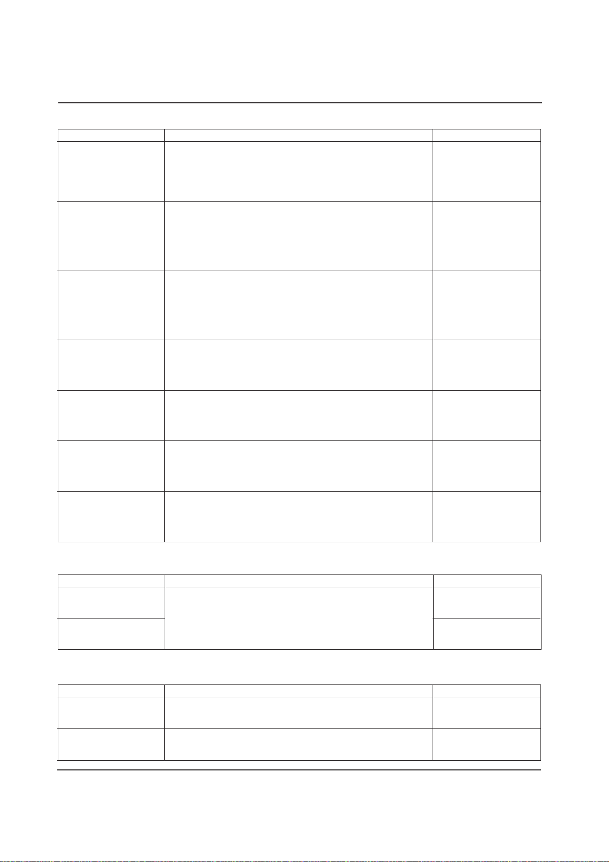
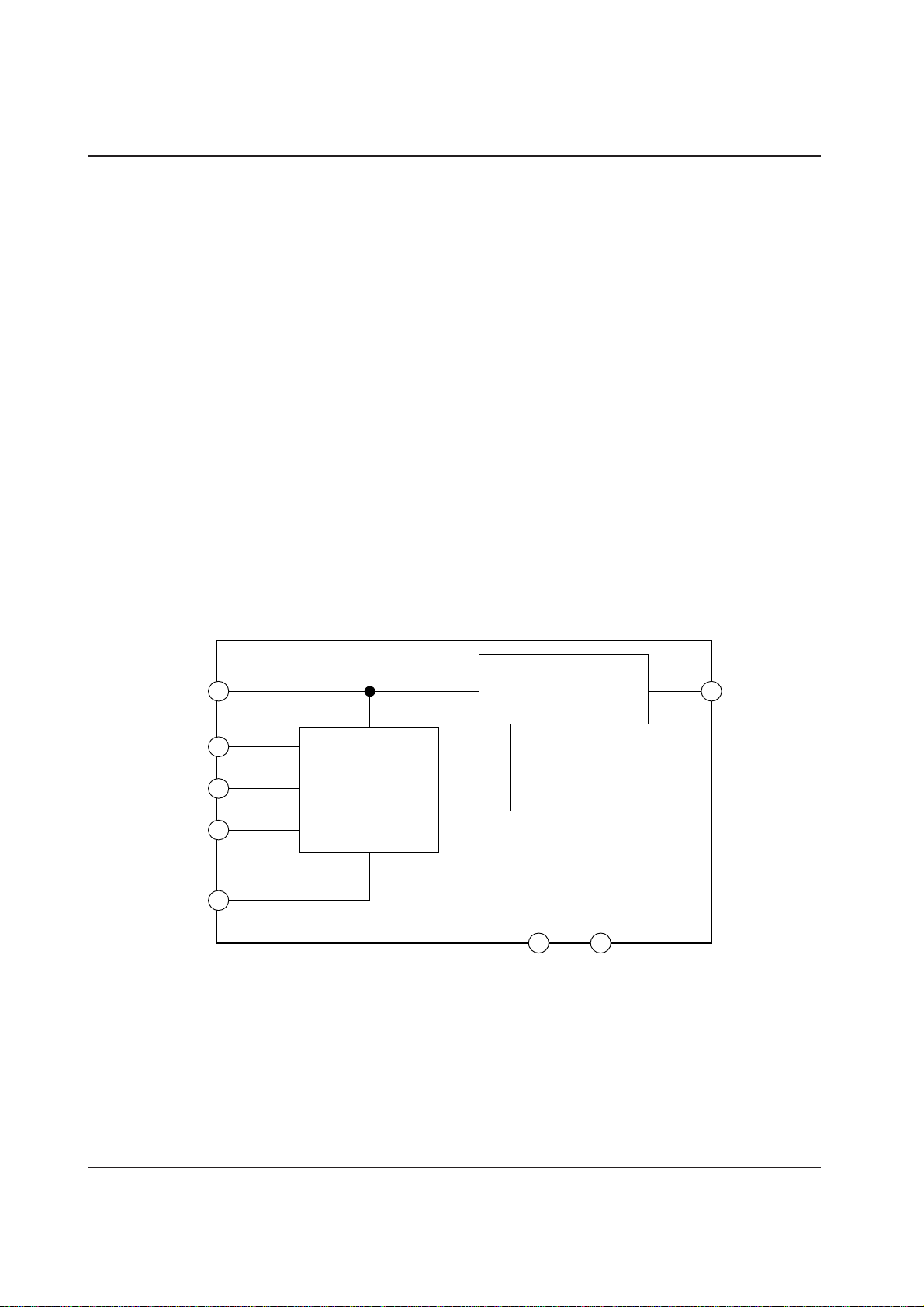
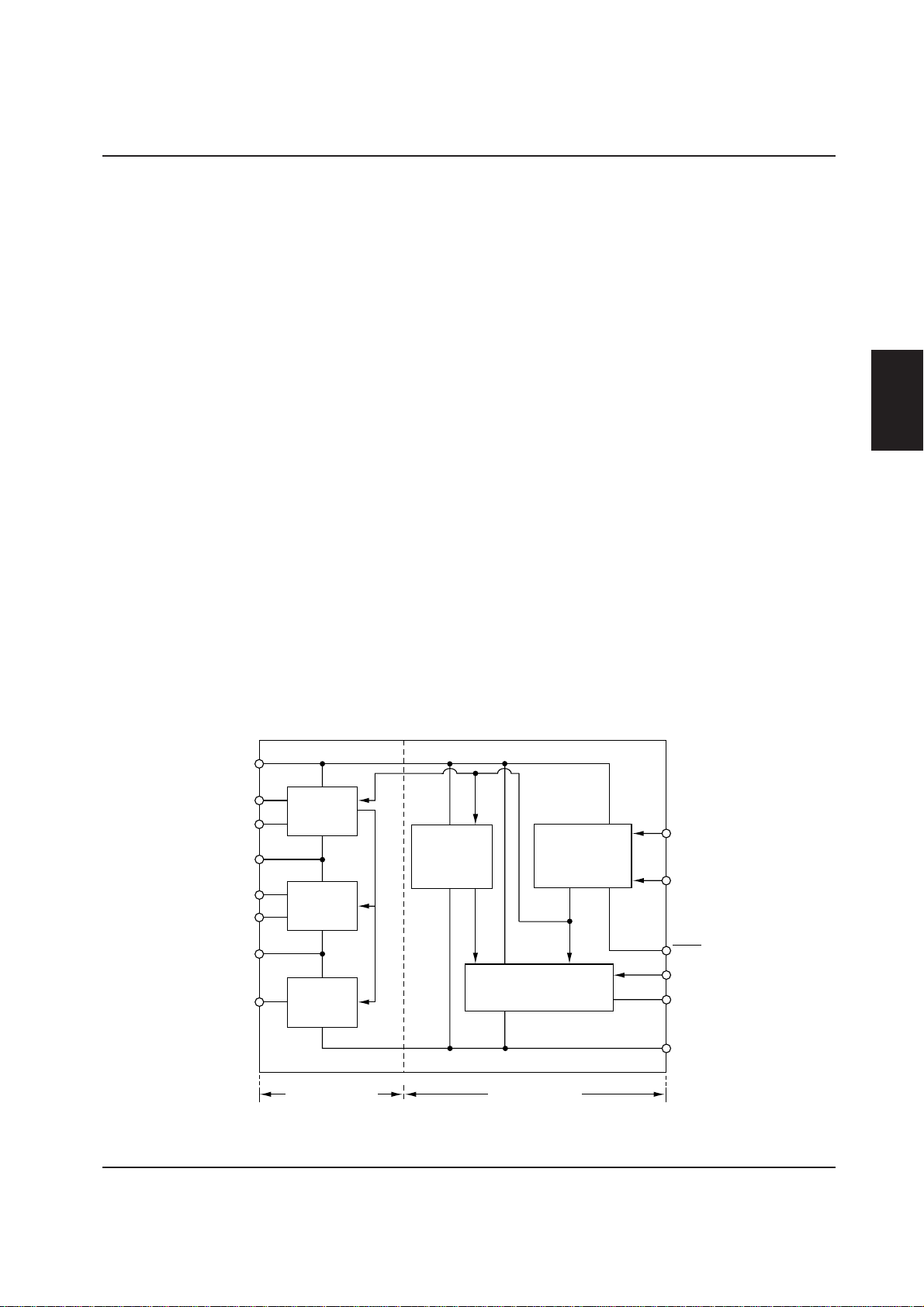
BLOCK DIAGRAM
V
DD
OSC1
OSC2
V
I
CR oscillator
Voltage converter
CAP1+
CAP1–
V
O
PIN ASSIGNMENTS
NC
OSC2
OSC1
DD
V
1
2
S1F76600M0B0
3
4
/C0B0
8
7
6
5
V
I
V
O
CAP1–
CAP1+
Series
S1F76600
PIN DESCRIPTIONS
Pin No. Pin name Description
1 NC No connection
2 OSC2 Resistor connection. Open when using external clock
3 OSC1 Resistor connection. Clock input when using external clock
4VDD Positive supply (system VCC)
5 CAP1+ Positive charge-pump connection
6 CAP1– Negative charge-pump connection
7VO ×2 multiplier output
8VI Negative supply (system ground)
S1F70000 Series EPSON 1–1
Technical Manual
Page 19
S1F76600 Series
SPECIFICATIONS
Absolute Maximum Ratings
Parameter Symbol Rating Unit
Input voltage range VI –10.0 to 0.5 V
Output voltage range VO Min. –20.0 V
Power dissipation PD
300 (DIP)
mW
150 (SOP)
Operating temperature range Topr –40 to +85 ˚C
Storage temperature range
Soldering temperature(for 10s). See note.
Tstg –65 to +150 ˚C
Tsol 260 ˚C
Note:
Temperatures during reflow soldering must remain within the limits set out in LSI Device Precautions.
Never use solder dip to mount S1F70000 series power supply devices.
Recommended Operating Conditions
V
DD = 0V, Ta = –40 to +85˚C unless otherwise noted
Parameter Symbol Condition Rating Unit
Min. Typ. Max.
ROSC = 1MΩ,
C1/C2≤1/20, C2≥10µF, — — –1.5
Oscillator startup voltage V
STA Ta = –20 to +85˚C V
See note 1.
ROSC = 1MΩ — — –2.2
Oscillator shutdown voltage
VSTP ROSC = 1MΩ –1.5 — — V
Load resistance RL
RL min
See note 2.
——Ω
Output current IO — — 30.0 mA
Clock frequency fOSC 10.0 — 30.0 kHz
CR oscillator network
resistance
R
OSC 680 — 2,000 kΩ
Capacitance C1, C2 3.3 — — µF
Notes:
1. The recommended circuit configuration for low-voltage operation (when V
I is between –1.2V and
–2.2V) is shown in the following figure. Note that diode D1 should have a maximum forward voltage of
0.6V with 1.0mA forward current.
2. R
L min can be varied depending on the input voltage.
1–2 EPSON S1F70000 Series
Technical Manual
Page 20
S1F76600 Series
3. RL min is a function of VI.
5
4
3
2
1
Minimum load resistance (kΩ)
0
1MΩ
1.0
V
1
2
3
4
STA1
Battery
1.5 2.0
Input voltage (V)
V
STA2
8
7
6
5
3.0
+
C2
22µF
C1
+
10µF
4.0 5.0 6.0
C
R
L
L
D1
Series
S1F76600
Electrical Characteristics
VDD = 0V, Ta = –40 to +85˚C unless otherwise noted
Parameter Symbol Condition Rating Unit
Min. Typ. Max.
Input voltage VI –8.0 — –1.5 V
Output voltage VO –16.0 — — V
Multiplier current IOPR
RL = ∞, ROSC = 1MΩ
V
I = –5V
—2030µA
Quiescent current IQ RL =∞, VI = –8V — — 2.0 µA
Clock frequency fOSC
ROSC = 1MΩ, VI = –5V
16 20 24 kHz
Output impedance RO IO = 10mA, VI = –5V — 75 100 Ω
Multiplication efficiency Peff IO = 5mA, VI = –5V 90 95 — %
OSC1 Input leakage current
S1F70000 Series EPSON 1–3
Technical Manual
ILKI VI = –8V — — 2.0 µA
Page 21
S1F76600 Series
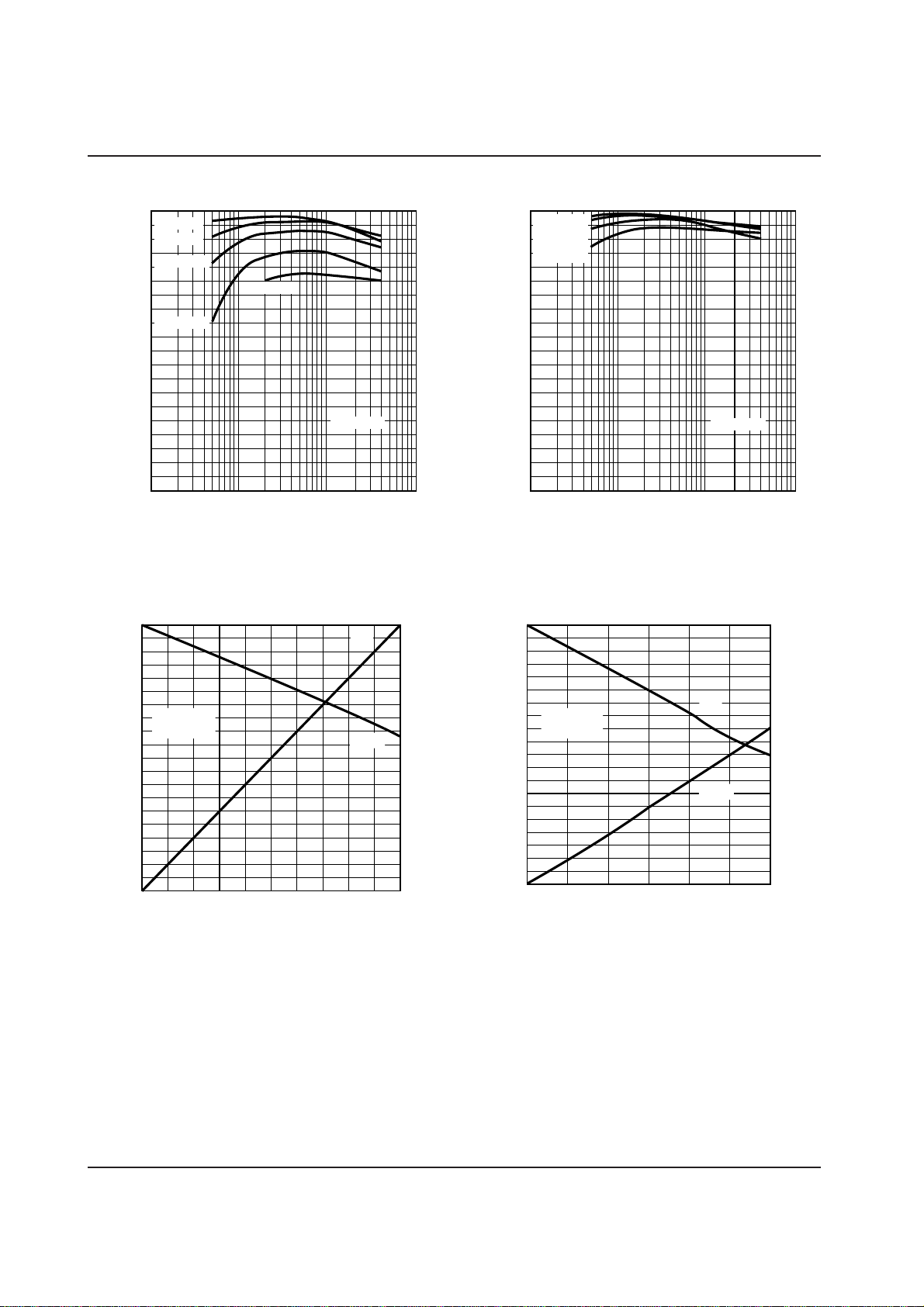
Typical Performance Characteristics
1000
Ta = 25°C
26
25
24
23
22
21
20
19
VI = –5.0V
I
= –3.0V
V
100
I = –5V
V
VI = –3V
V
I = –2V
18
I
= –2.0V
V
fOSC [kHz]
10
17
16
fOSC [kHz]
15
14
13
12
11
10
9
1
10 100 1000 10000
ROSC [kΩ]
8
–40 –20 0 20 40
Ta [°C]
60 80 100
(1) Clock frequency vs. External resistance (2) Clock frequency vs. Ambient temperature
50
f
OSC
45
= 40kHz
40
Ta = 25°C
35
f
OSC
=
20kHz
30
[µA]
25
f
OSC
OPR
l
20
=
10kHz
15
10
5
0
–7 –6 –5 –4 –3 –2 –1 0
VI [V]
0
Ta = 25˚C
I
= –5.0V
V
–5
[V]
O
V
–10
–15
0 1020304050
IO [mA]
(3) Multiplier current vs. Input voltage (4) Output voltage vs. Output current
1–4 EPSON S1F70000 Series
Technical Manual
Page 22
S1F76600 Series
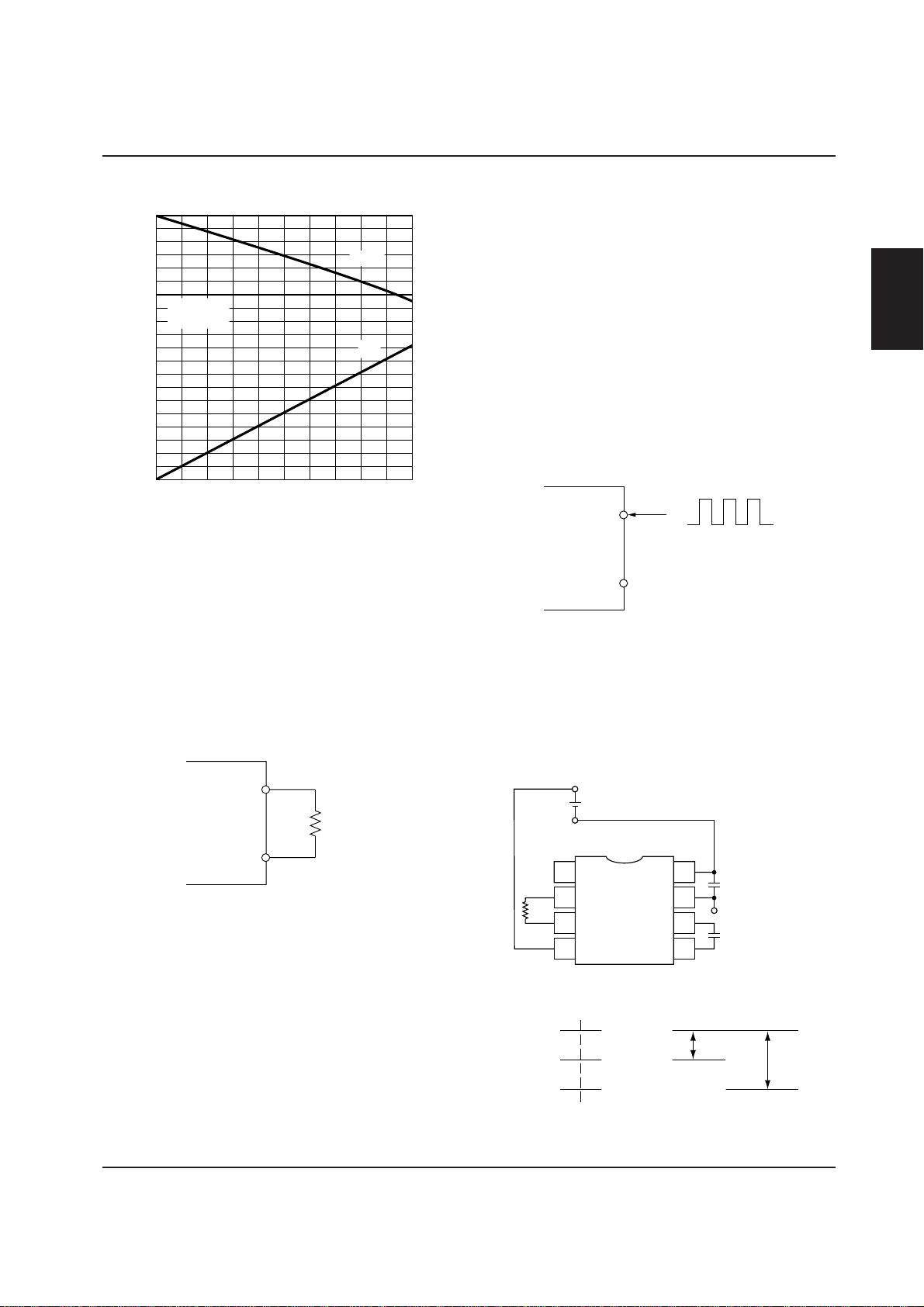
0
Ta = 25°C
V
I
= –3.0V
0
–1
Ta = 25°C
V
I
= –2.0V
–2
[V]
–3
[V]
O
V
–5
O
V
–4
–5
–10
0102030
IO [mA]
–6
0 23456789101
IO [mA]
(5) Output voltage vs. Output current (6) Output voltage vs. Output current
300
Ta = 25°C
O = 7mA
I
300
Ta = 25°C
O = 10mA
I
Series
S1F76600
200
RO [Ω]
100
0
–7 –6 –5 –4 –3 –2 –1 0
VI [V]
200
RO [Ω]
100
0
–7 –6 –5 –4 –3 –2 –1 0
VI [V]
(7) Output impedance vs. Input voltage (8) Output impedance vs. Input voltage
S1F70000 Series EPSON 1–5
Technical Manual
Page 23
S1F76600 Series
100
IO = 2mA
IO = 5mA
90
IO = 10mA
80
70
60
IO = 20mA
IO = 30mA
50
Peff [%]
40
30
20
10
0
1 10 100 1000
fOSC [kHz]
(9) Multiplication efficiency vs. (10) Multiplication efficiency vs.
Clock frequency Clock frequency
100
90
80
70
Ta = 25°C
V
I
60
50
Peff [%]
40
30
20
10
= –5.0V
0
0
10 20 30 40 50
IO [mA]
VI = –5.0V
I
I
Peff
100
90
80
70
60
50
40
30
20
10
0
[mA]
I
I
100
IO = 0.5mA
I
O
= 1.0mA
90
IO = 2.0mA
I
O
= 4.0mA
80
70
60
50
Peff [%]
40
30
20
VI = –3.0V
10
0
1 10 100 1000
f
OSC
[kHz]
100
90
80
I
70
60
Ta = 25°C
V
I
= –3.0V
I
50
40
Peff [%]
Peff
30
20
10
0
0 5 10 15 20 25 30
IO [mA]
100
90
80
70
60
50
40
30
20
10
0
[mA]
I
I
(11) Multiplication efficiency/input current (12) Multiplication efficiency/input current
vs. Output current vs. Output current
1–6 EPSON S1F70000 Series
Technical Manual
Page 24
S1F76600 Series
100
90
80
70
Ta = 25°C
V
I = –2.0V
60
50
Peff [%]
40
30
20
10
0
012345678910
IO [mA]
Peff
II
40
36
32
28
24
20
16
12
8
4
0
(13) Multiplication efficiency/input current
vs. Output current
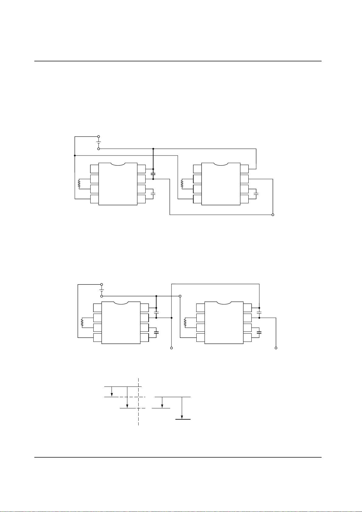
FUNCTIONAL DESCRIPTIONS
CR Oscillator
S1F76600 has a built-in CR oscillator as the internal oscillator, and an external oscillation resistor R
nected between the pins OSC1 and OSC2 before operation.
OSC is con-
far as the
straight portion (500kΩ < R
R
OSC = A • (1/fOSC)
(A : Constant, When GND is 0V and V
approximately 2.0 × 10
So, the R
I [mA]
I
(Recommended oscillation frequency : 10kHz to 30kHz
(R
OSC value can be obtained from this formula.
OSC : 2MΩ to 680kΩ))
OSC < 2MΩ) is concerned:
10
(I/F).)
DD is 5V, A is
When the external clock operates, make the pin OSC2
open as shown below and input the 50% duty of the external clock from the pin OSC1.
OSC1
External clock
OSC2
Open
Voltage Multiplier
The voltage multiplier uses the clock signal from the
oscillator to double the input voltage. This requires two
external capacitors—a charge-pump capacitor, C1, between CAP1+ and CAP1–, and a smoothing capacitor,
C2, between V
I and VO.
Series
S1F76600
= 0 V
V
OSC1
(Note 1)
OSC
R
V
= –5 V
I
DD
5 V
OSC2
8
+
C2
10µF
7
6
5
+
= –10V (2VI)
V
O1
C1
10µF
Note 1
Since the oscillation frequency varies with wiring ca-
1
2
1MΩ
3
4
pacitance, make the cables between the terminals OSC1
and OSC2 and R
When setting the external resistor R
able for f
OSC that brings about the maximum efficiency
from characteristics graph (9) and (10). The relations
between R
expressed approximately with the following formula as
S1F70000 Series EPSON 1–7
Technical Manual
OSC as short as possible.
OSC, find ROSC suit-
OSC and fOSC in characteristics graph (1) are
Doubled potential levels
V
CC
(+5V)
GND
(–5V)
DD
= 0 V
V
I
= –5 V
V
VO = (2VI) = –10 V
Page 25
S1F76600 Series
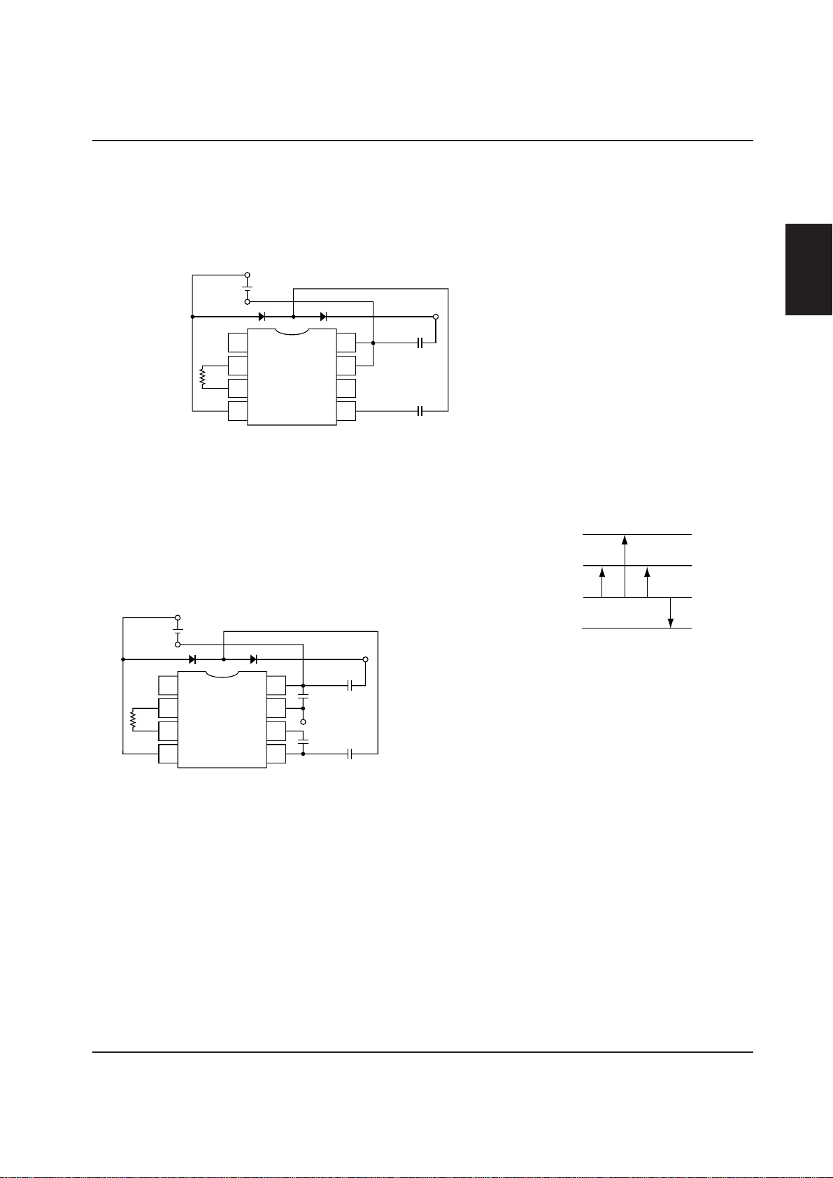
TYPICAL APPLICATIONS
Parallel Connection
Connecting two or more chips in parallel reduces the
output impedance by 1/n, where n is the number of devices used.
V
= 0 V
DD
V
= –5 V
I
5 V
1
2
1MΩ
3
4
8
+
C2
10µF
7
6
C1
+
10µF
5
Serial Connection
Connecting two or more chips in series obtains a higher
output voltage than can be obtained using a parallel
V
= 0 V
DD
= –5 V
V
I
1MΩ
5 V
1
2
3
4
8
+
C2
10µF
7
6
C1
+
10µF
5
1
2
1MΩ
3
4
8
7
6
C1
+
10µF
5
= –10 V
V
O
connection, however, this also raises the output impedance.
' = VI = –5
V
DD
1
2
1MΩ
3
4
8
+
C2
10µF
7
6
C1
+
10µF
5
V
= –10 V = VI'
V
O
' = –15 V
O
Potential levels
V
DD
(0 V)
I
(–5 V)
V
O
(–10 V)
V
Primary stage Secondary stage
VDD'
I
V
'
O
' (–15 V)
V
1–8 EPSON S1F70000 Series
Technical Manual
Page 26
Positive Voltage Conversion
Diodes can be added to a circuit connected in parallel to
make a negative voltage positive.
= 0 V
V
DD
V
= –5 V
I
1MΩ
5 V
V
1
2
3
4
8
7
6
5
Simultaneous Voltage Conversion
Combining a multiplier circuit with a positive voltage
conversion circuit generates both –10 and 3.8 V outputs
from a single input.
' = 3.8 V
O
C2
+
10µF
C1
+
10µF
Potential levels
V
O2
= 3.8 V
S1F76600 Series
Series
S1F76600
= –5 V
V
I
1MΩ
1
2
3
4
VDD = 0 V
5 V
V
DD
= 0 V
I
= –5 V
V
O1
= –10 V
V
V
= 3.8 V
O2
C2
10µF
V
O1
C1
10µF
C4
10µF
= –10 V
C3
10µF
++
+
8
7
6
+
5
S1F70000 Series EPSON 1–9
Technical Manual
Page 27
S1F76620 Series
S1F76620 Series CMOS DC/DC Converter (Voltage Doubler)
DESCRIPTION
S1F76620 is a high efficiency and low power consumption CMOS DC/DC converter. It enables to obtain 2
times step-up output (3.0 to 16V) from input voltage
(1.5 to 8V). Also, S1F76620 enable to drive ICs (liquid
crystal driver, analog IC, etc.), which require another
power supply in addition to logic main power supply,
with a single power supply, and it is suitable for micro
power IC of hand-held computers, handy devices, etc.
due to its small power consumption.
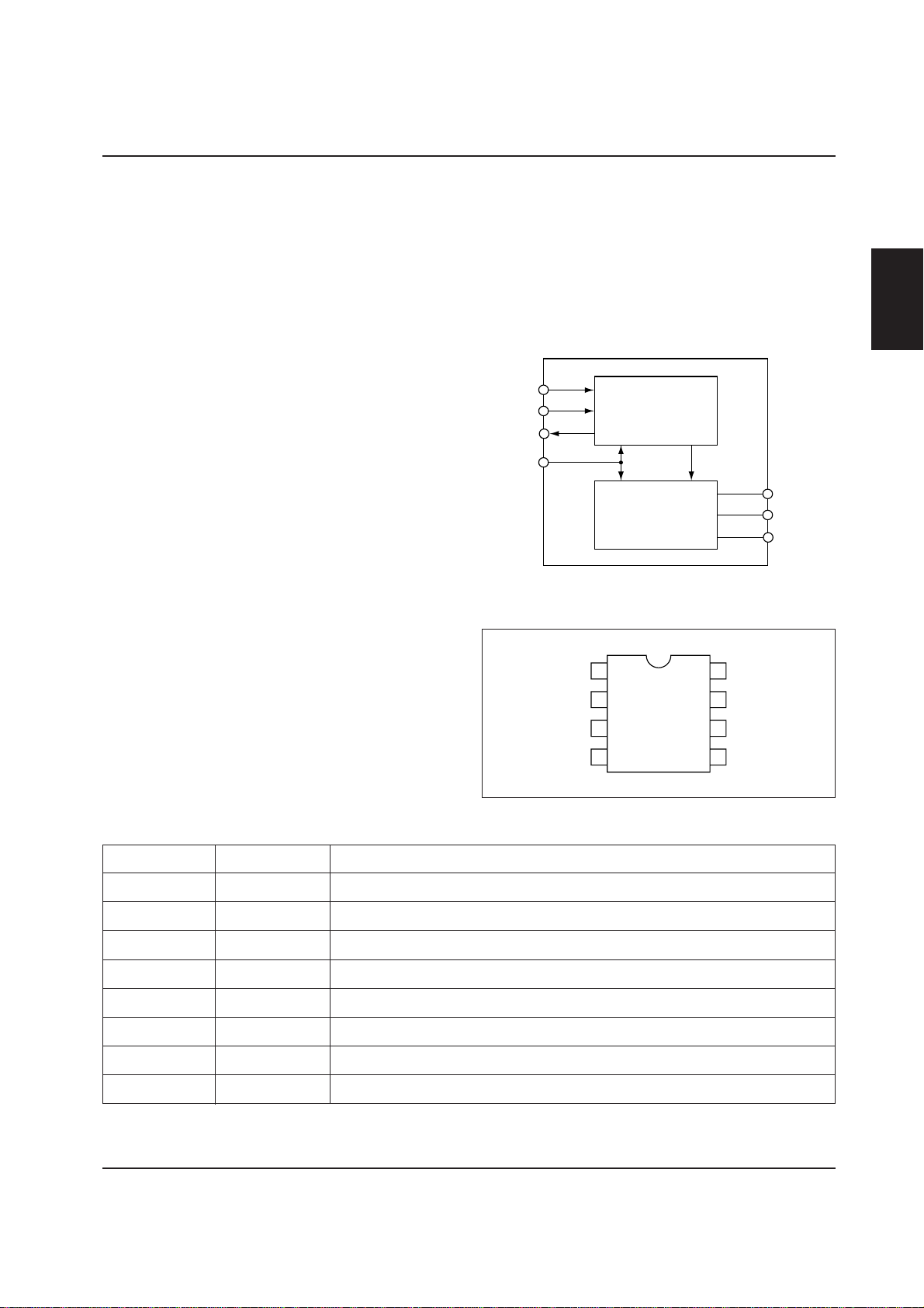
BLOCK DIAGRAM
V
DD
FEATURES
(1) High efficiency and low power consumption
CMOS DC/DC converter
(2) Easy voltage conversion from input voltage V
to positive potential side or negative potential side
• Input V
2V
DD (5V) to output –VDD (–5V),
DD (10V)
(3) Output current : Max. 30mA
(V
DD = 5V)
(4) Power conversion efficiency : Typ. 95%
(5) Possibility of series connection
(In 2-piece use, V
DD = 5V, VO = 15V)
(6) Low voltage operation : Suitable for
battery drive
(7) Built-in CR oscillator
(8) SOP4-8pin······························ S1F76620M0A0
Bare Chip ······························· S1F76620D0A0
Voltage conversion circuit
DD (5V)
V
O
OSC1
OSC2
P
OFF
GND
CR oscillator
CAP1+ CAP1–
1–10 EPSON S1F70000 Series
Technical Manual
Page 28
PIN DESCRIPTIONS
Pin Assignments
S1F76620 Series
Pin descriptions
Pin No.
1
2
3
Pin name
POFF
GND (VSS)
OSC1
POFF
GND
OSC1
OSC2
1
2
3
4
8
7
6
5
O
V
CAP1+
CAP1–
V
DD
Pin Assignments of SOP4-8pin
Description
Input pin for power off control.
Power pin. (Minus side, System GND)
Oscillation resistor connection pin. Works as the clock input pin when the
external clock operates.
Series
S1F76620
4
5
6
7
8
S1F70000 Series EPSON 1–11
Technical Manual
OSC2
VDD
CAP1–
CAP1+
VO
Oscillation resistor connection pin. Opens when the external clock operates.
Power pin. (Plus side, System VCC)
Pump up capacitor minus side connection pin for 2 times step-up.
Pump up capacitor plus side connection pin for 2 times step-up.
Output pin at the time of 2 times step-up.
Page 29
S1F76620 Series
Pad Center Coordinates (S1F76620D0A0)
Pad No.
1
2
3
4
5
6
7
8
9
10
11
12
13
14
15
16
17
Pad name
(NC)
(NC)
POFF
(NC)
(NC)
(NC)
GND (VSS)
OSC1
OSC2
VDD
CAP1–
CAP1+
(NC)
VO
(NC)
(NC)
(NC)
Pad center
coordinates
µm)
X (
–984
984
coordinates
Pad center
µm)
Y (
1096
788
580
390
96
–218
–510
–802
–1094
–1134
–892
–514
182
372
750
942
1134
Description
—
—
Input pin for power off control
—
—
—
Power input pin (Minus side)
Oscillation resistor connection pin
Oscillation resistor connection pin
Power input pin (Plus side)
Pump up capacitor minus side connection pin for 2
times step-up
Pump up capacitor plus side connection pin for 2
times step-up
—
2 times step-up output pin
—
—
—
Chip External Shape
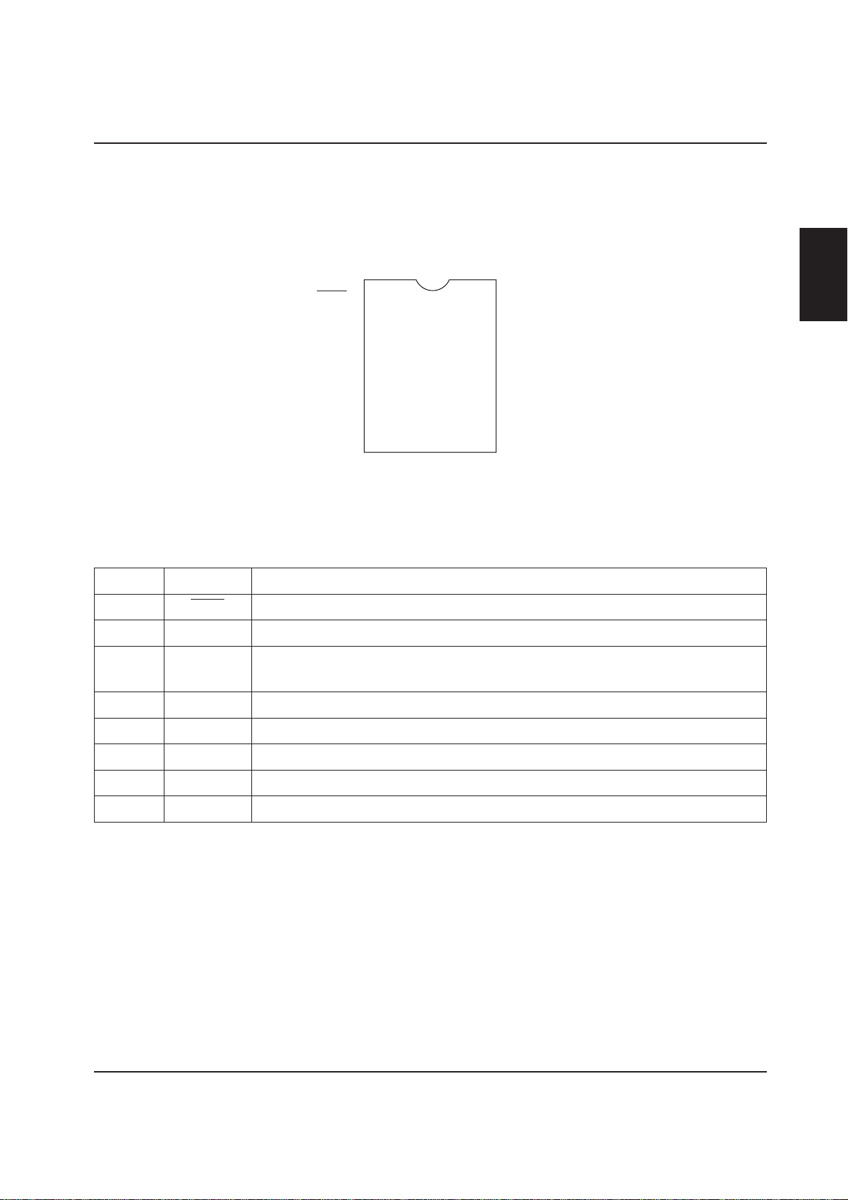
Y
+
(0,0)
2.30mm
Pad Assignment
Pad aperture : 100µm × 100µm Chip thickness : 400µm
Note
Do not bond the NC pad.
X
2.60mm
1–12 EPSON S1F70000 Series
Technical Manual
Page 30
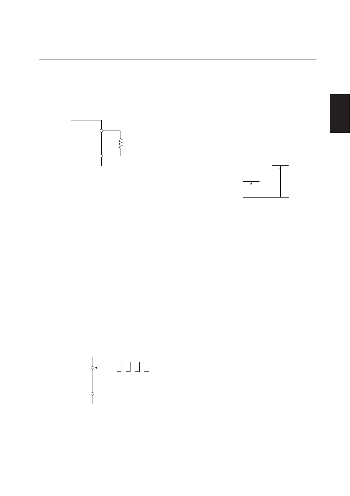
FUNCTIONAL DESCRIPTIONS
CR Oscillator
S1F76620 has a built-in CR oscillator as the internal oscillator, and an external oscillation resistor R
nected between the pins OSC1 and OSC2 before operation.
OSC1
OSC2
(Note 1)
R
OSC is con-
OSC
S1F76620 Series
Voltage Conversion Circuit
The voltage conversion circuit uses clocks generated in
the CR oscillator to double the input supply voltage
V
DD.
In case of 2 times step-up, 2 times voltage (2V
the input voltage is obtained from the V
pump up capacitor is connected between CAP1+ and
CAP2– and a smoothing capacitor is connected between V
When GND is 0 and V
DD and VO outside.
DD is 5, the relations between
input/output and voltage are as shown below:
CAP1=2VDD=10V
DD) of
O pin when a
Series
S1F76620
Note 1
Since the oscillation frequency varies with wiring capacitance, make the cables between the terminals OSC1
and OSC2 and R
When setting the external resistor R
able for f
OSC that brings about the maximum efficiency
OSC as short as possible.
OSC, find ROSC suit-
from characteristics graph (9) and (10). The relations
between R
OSC and fOSC in characteristics graph (1) are
expressed approximately with the following formula as
far as the
straight portion (500kΩ < R
R
OSC = A • (1/fOSC)
(A : Constant, When GND is 0V and V
approximately 2.0 × 10
So, the R
OSC value can be obtained from this formula.
OSC < 2MΩ) is concerned:
10
(I/F).)
DD is 5V, A is
(Recommended oscillation frequency : 10kHz to 30kHz
(R
OSC : 2MΩ to 680kΩ))
When the external clock operates, make the pin OSC2
open as shown below and input the 50% duty of the ex-
ternal clock from the pin OSC1.
V
DD
=5V
G
ND
=0V
OSC1
External clock
OSC2
S1F70000 Series EPSON 1–13
Technical Manual
Open
Page 31
S1F76620 Series
ELECTRICAL CHARACTERISTICS
Absolute Maximum Ratings
(Ta = –40 to +85°C)
Parameter
Input supply voltage
Input pin voltage
Output voltage
Output supply voltage
Output pin voltage
Allowable loss
Operating temperature
Storage temperature
Note 1
Under the conditions exceeding the above absolute maximum ratings, the IC may result in a permanent destruction.
An operation for a long period under the conditions of the above absolute maximum ratings may deteriorate the
reliability remarkably.
Note 2
All voltage values are based on GND being 0V.
Symbol
VIN
VI
VO
VCAP+
VCAP–
PD
Topr
Tstg
Min.
–0.5
–0.5
—
–0.5
–0.5
—
–40
–65
Rating
Max.
10.0
VDD + 0.5
20
VDD + 0.5
VO + 0.5
300
150
85
150
Unit
V
V
V
V
V
mW
°C
°C
Remarks
—
OSC1, OSC2
—
CAP+
CAP–
DIP-8pin
SOP-8pin
—
—
1–14 EPSON S1F70000 Series
Technical Manual
Page 32

Recommended Operating Conditions
S1F76620 Series
(Ta = –40 to +85°C)
Parameter
Symbol
Min.
Max.
Unit
ROSC = 1MΩ
Rating
Step-up start operation
Step-up stop voltage
VSTA1
VSTA2
VSTP
1.5
2.2
—
—
—
1.5
V
V
V
C
See note 2.
ROSC = 1MΩ
ROSC = 1MΩ
RLmin
Output load resistance
Output load current
Oscillation frequency
RL
IO
fOSC
See note 3.
—
10
—
30
30
Ω
mA
kHz
External resistor for
oscillation
Step-up capacitor
ROSC
C1, C2
680
3.3
2000
—
kΩ
µF
Note 1
All voltages are based on the GND being 0V.
Note 2
The figure below shows the recommended circuit for operation with low voltages (V
Remarks
2 ≥ 10µF CL/C2 ≥ 1/20
—
—
—
—
—
DD = 1.5 to 2.2V):
Series
S1F76620
C
*D
L
1
R
L
1
P
OFF
2
GND
3
OSC1
4
OSC2
* (DI (VF (IF=1mA) is recommended to be not more than 0.6V.)
CAP1+
CAP1–
8
O
V
7
6
5
V
DD
+
C
1
+
–
–
C
2
Recommended Circuit
Note 3
Lmin varies with input voltage. See Characteristics Graph (15).
R
S1F70000 Series EPSON 1–15
Technical Manual
Page 33

S1F76620 Series
Electrical Characteristics
(V
DD = 5V, Ta = –40 to +85°C)
Parameter
Symbol
Min.
Input supply voltage
Output voltage
VDD
VO
1.8
—
Step-up circuit current
consumption
Static current
Oscillation frequency
Output impedance
IOPR
IQ
fOSC
RO
—
—
16
—
Step-up power conversion efficiency
Input leak current
Peff
ILKI
90
—
Note 1
All voltage values are based on GND being 0V.
Rating
Typ.
—
—
35
—
20
85
95
—
Max.
8.0
16.0
50
1.0
24
130
—
1.0
Unit
V
V
µA
µA
kHz
Ω
%
µA
Remarks
—
—
ROSC = 1MΩ
—
ROSC = 1MΩ
IO = 10mA
IO = 5mA
OSC1 pin
1–16 EPSON S1F70000 Series
Technical Manual
Page 34

Characteristics Graph
S1F76620 Series
1000
Ta=25°C
VDD=5V
100
[kHz]
VDD=3V
OSC
f
10
VDD=2V
1
10 100 1000 10000
OSC
[kΩ]
R
(1) Oscillation frequency vs.
External resistance for oscillation
100
80
60
[µA]
40
OPR1
I
20
0
Ta=25°C
C
1=C2
=10µF
f
OSC
=40kHz
f
OSC
=20kHz
f
OSC
=10kHz
0123456
VDD[V]
30
28
26
24
22
20
[kHz]
OSC
18
f
VDD=5V
16
14
12
VDD=2V
VDD=3V
10
–40 –20 0 20 40 60 80 100
Ta[°C]
(2) Oscillation frequency vs. Temperature
10
9
8
7
6
[V]
5
O
V
4
3
Ta=25°C
2
V
DD
1
0
0 5 10 15 20 25 30
1=C2
C
=5V
=10µF
IO [mA]
Series
S1F76620
(3) Step-up circuit current consumption vs.
(4) Output voltage (V
O) vs. Output current 1
Input current
S1F70000 Series EPSON 1–17
Technical Manual
Page 35

S1F76620 Series
6
4
5
3
4
[V]
O
V
3
[V]
O
V
2
2
Ta=25°C
1
V
DD
=3V
C
1=C2
=10µF
0
0 5 10 15 20
1
Ta=25°C
V
DD
=2V
C
1=C2
=10µF
0
012345678910
IO [mA] IO [mA]
(5) Output voltage (VO) vs. Output current 2 (6) Output voltage (VO) vs. Output current 3
300
250
300
250
Ta=25°C
I
O
=10mA
200
[Ω]
150
O
R
100
50
Ta=25°C
O
=5mA
I
0
0123456
DD
[V]
V
200
[Ω]
150
O
R
100
50
0
0123456
DD
[V]
V
(7) Output impedance vs. Input current 1 (8) Output impedance vs. Input voltage 2
1–18 EPSON S1F70000 Series
Technical Manual
Page 36

S1F76620 Series
100
90
80
70
60
50
Peff[%]
40
30
20
10
Ta=25°C
V
DD=5V
C1=C2=10µF
0
0 102030
I
O [mA]
(9) Step-up power conversion efficiency vs.
Output current 1
Input current vs. Output current 1
100
90
80
70
60
50
Peff[%]
40
30
20
10
0
Ta=25°C
V
DD
=5V
C1=C2=10µF
012345678910
O
[mA]
50
40
30
20
10
0
150
120
90
60
30
0
DD[mA]
I
[mA]
DD
I
100
90
80
70
60
50
Peff[%]
40
30
20
10
Ta=25°C
V
DD=3V
C1=C2=10µF
0
0 5 10 15 20
I
O [mA]
(10) Step-up power conversion efficiency vs.
Output current 2
Input current vs. Output current 2
100
90
80
Peff[%]
70
60
50
1 10 100 1000
IO =5mA
IO =2mA
IO =20mA
focs[kHz]I
IO =10mA
Ta=25°C
V
DD
=5V
1=C2
=10µF
C
100
90
80
70
60
50
40
30
20
10
Series
S1F76620
DD[mA]
I
0
(11) Step-up power conversion efficiency vs.
Output current 3
. (12) Step-up power conversion efficiency vs.
Oscillation frequency 1
Input current vs. Output current 3
S1F70000 Series EPSON 1–19
Technical Manual
Page 37

S1F76620 Series
100
90
80
IO =1mA
IO =5mA
Peff[%]
70
60
IO =2mA
IO =10mA
Ta=25°C
V
C
DD
=3V
1=C2
=10µF
50
1 10 100 1000
focs[kHz]
(13) Step-up power conversion efficiency vs.
Oscillation frequency 2
1.7
1.6
[V]
STA1
V
1.5
1.4
1.3
1.2
Ta=25°C
C
1=C2
=10µF
OSC
=1MΩ
R
100
90
IO =0.5mA
80
IO =1mA
IO =2mA
Peff[%]
70
60
IO =5mA
Ta=25°C
V
DD
=2V
1=C2
=10µF
C
50
1 10 100 1000
focs[kHz]
(14) Step-up power conversion efficiency vs.
Oscillation frequency 3
1.1
1.0
0.9
100 1000 10000 100000
R
L
[Ω]
(15) Step-up start voltage (1) vs. Load resistance
1–20 EPSON S1F70000 Series
Technical Manual
Page 38

EXAMPLE OF REFERENCE EXTERNAL CONNECTION
2 Times Step-up
2 times step-up output of V
O (2 × VDD) is obtained from the circuit shown in Figure 1.
S1F76620 Series
1
POFF
2
GND
3
4
OSC1
OSC2
VI
Figure 1 2 Time Step-up Operation
Parallel Connection
It is possible to make the output impedance (R
O) small when several pieces of the circuit shown in Figure 1 are
connected. Parallel connection of n circuits reduces R
C
2 can be commonly used.
1
P
OFF
2
GND
V
I
3
OSC1
CAP1+
CAP1–
8
O
V
7
6
OFF
•
2 VI
V
CAP1+
8
O
7
+
8
O
V
CAP1+
CAP1–
O to 1/n approximately. One piece of the smoothing capacitor
7
6
5
V
DD
+
+
–
–
1
P
2
GND
_
3
OSC1
CAP1–
6
+
4
+
_
OSC2
5
V
DD
_
Series
S1F76620
4
OSC2
5
V
DD
Figure 2 Parallel Connection
S1F70000 Series EPSON 1–21
Technical Manual
Page 39

S1F76620 Series
Series Connection
When S1F76620 is connected in series (V
stage respectively), the output voltage can be increased more. But the series connection makes the output impedance
high. Figure 3 shows an example of the series connection to get V
DD and VO in the previous stage are connected to GND and VDD in the next
O = 15V from VDD = 5V.
• •
V o=2 V
I
1
P
OFF
2
GND
1
P
OFF
2
GND
V
I
3
4
OSC1
OSC2
CAP1+
CAP1–
8
V
O
3
OSC1
7
6
5
DD
V
+
4
+
–
OSC2
–
CAP1+
CAP1–
8
V
O
7
6
5
DD
V
+
–
V o'=3 V
+
–
I
Figure 3 Series Connection
DD(5V)
V
V
O=10V
First stage Next stage
VDD'
GND'
V
O'=15V
GND(0V)
Figure 4 Power Supply Relations in Series Connection (1)
Note
When the input voltage in the next stage is as per the specification (V
output in the first stage (V
V
DD
GND(0V)
O-VDD) can be used as the input in the next stage (VDD-GND). (See Figure 5.)
First stage
O
=4V
V
Next stage
(2V)
DD-GND ≤ 8V) in a series connection, the
V
O
'=8V
VDD'
GND'
Figure 5 Power Supply Relations in Series Connection (2)
1–22 EPSON S1F70000 Series
Technical Manual
Page 40

S1F76620 Series
Negative Voltage Conversion
S1F76620 can boost input voltage to twice on the positive potential side by using the circuit shown in Figure 6. But
the output voltage drops by the forward voltage V
shown in Figure 6 for example, V
O is calculated as follows: VO = –5V + 2 × 0.6V = –3.8V.
F of the diode. When GND is 0V, VDD is 5V and VF is 0.6V as
1
P
OFF
O
V
+–
8
Series
S1F76620
2
3
4
GND
OSC1
OSC2
CAP1+
CAP1–
7
+–
6
5
DD
V
VO'
Figure 6 Negative Voltage Conversion
Negative Voltage Conversion + Positive Voltage Conversion
When the 3 times step-up operation shown in Figure 1 and the positive voltage conversion in Figure 6 are combined,
the circuit shown in Figure 7 can be formed and 10V and –3.8V can be obtained from the input 5V. However, the
output impedance is higher than in case of connection of either one only (the negative voltage conversion or the
positive voltage conversion).
V
1
2
3
P
OFF
GND
OSC1
V
CAP1+
CAP1–
O1
8
O
7
+
+
–
–
6
Potential Relations Diagram
2 V
I
V
DD
V
I
V
SS
–VI+2 V
•
F
4
OSC2
5
DD
V
V
O2
V
O2
Figure 7 Negative Voltage Conversion + Positive Voltage Conversion
S1F70000 Series EPSON 1–23
Technical Manual
Page 41

S1F76620 Series
MEASUREMENT CIRCUIT
V
O
I
O
A
R
L
1
P
OFF
8
O
V
V
2
3
4
GND
OSC1
OSC2
V
I
OPR
A
R
OSC
V
I
CAP1+
CAP1–
7
6
5
V
DD
+
C
1
+
2
–
C
–
1–24 EPSON S1F70000 Series
Technical Manual
Page 42

MECHANICAL DATA
S1F76620 Series
S1F76620M0A0 SOP4-8pin
D
85
E
HE
θ2
2
A
A
1
A
θ3
Max.
5.2
—
0.45
0.25
Symbol
E
D1
A
A1
A2
e
b
C
INDEX
14
e
b
Dimension in Milimeters
Min.
4.8
—
Nom.
5
—
1.75
0.15
1.6
1.27
0.25
0.05
0.35
0.15
θ
L
0.55
L1
L2
HE
D
6.4
4.8
6.8
5
7.2
5.2
θ2
θ3
R
R1
* for reference
Note
This drawing is subject to change without notice for improvement.
θ
Min.
(0.189)
—
(0.010)
(0.002)
(0.252)
(0.189)
R
1
R
C
L
2
L
L
1
Dimension in Inches*
Nom.
(0.197)
—
(0.069)
(0.006)
(0.063)
(0.050)
(0.014)
(0.006)
(0.022)
(0.268)
(0.197)
Reference
Max.
(0.204)
—
(0.017)
(0.009)
(0.283)
(0.204)
Series
S1F76620
S1F70000 Series EPSON 1–25
Technical Manual
Page 43

2. DC/DC Converter & Voltage Regulator
Page 44
S1F76610 Series
S1F76610 Series CMOS DC/DC Converter (Voltage
Doubler / Tripler) & Voltage Regulator
DESCRIPTION
The S1F76610 Series is a highly effecient CMOS DC/
DC converter for doubling or tripling an input voltage.
It incorporates an on-chip voltage regulator to ensure
stable output at the specified voltage. The S1F76610
Series offers a choice of three, optional temperature
gradients for applications such as LCD panel power
supplies.
The S1F76610C0B0 is available in 14-pin plastic DIPs,
the S1F76610M0B0, in 14-pin plastic SOPs, and the
S1F76610M2B0 in 16-pin plastic SSOPs.
FEATURES
• 95% (Typ.) conversion efficiency
• Up to four output voltages, V
voltage, V
I
• On-chip voltage regulator
• 20mA maximum output current at V
• Three temperature gradients : –0.1, –0.4 and –0.6%/
°C
O, relative to the input
I = –5V
• External shut-down control
•2µA maximum output current when shut-down
• Two-in-series configuration doubles negative output
voltage.
• On-chip RC oscillator
• S1F76610C0B0 ...... Plastic DIP-14 pin
S1F76610M0B0...... Plastic SOP5-14 Pin
S1F76610M2B0...... Plastic SSOP2-16 pin
APPLICATIONS
• Power supplies for LCD panels
• Fixed-voltage power supplies for battery-operated
equipment
• Power supplies for pagers, memory cards, calculators
and similar hand-held equipment
• Fixed-voltage power supplies for medical equipment
• Fixed-voltage power supplies for communications
equipment
• Power supplies for microcomputers
• Uninterruptable power supplies
Series
S1F76610
BLOCK DIAGRAM
V
DD
OSC1
OSC2
V
I
CAP1–
CAP1+
CAP2–
CAP2+
CR
oscilator
Voltage
multiplier
(1)
Voltage
multiplier
(2)
Multiplication
stage
Reference
voltge
generator
Temperature
gradient
selector
Voltage regulator
Stabilization
stage
TC1
TC2
P
OFF
RV
V
REG
V
O
S1F70000 Series EPSON 2–1
Technical Manual
Page 45

S1F76610 Series
PIN ASSIGNMENTS
TC1
TC2
1
2
3
4
5
6
7
I
V
CAP+
CAP–
CAP2+
CAP2–
PIN DESCRIPTIONS
S1F76610C0B0/M0B0
Pin No.
1
2
3
4
5
6
7
8
9
10
11
12
13
14
Pin name
CAP1+
CAP1–
CAP2+
CAP2–
TC1
TC2
I
V
VO
VREG
RV
POFF
OSC2
OSC1
DD
V
NC
TC1
TC2
V
1
2
3
4
5
6
7
8
I
16
15
14
13
12
11
10
9
VDD
OSC1
NC
OSC2
OFF
P
RV
REG
V
VO
14
13
12
11
10
9
8
VDD
OSC1
OSC2
OFF
P
RV
VREG
VO
CAP+
CAP–
CAP2+
CAP2–
S1F76610M2B0S1F76610C0B0/M0B0
Description
Positive charge-pump connection for ×2 multiplier
Negative charge-pump connection for ×2 multiplier
Positive charge-pump connection for ×3 multiplier
Negative charge-pump connection for ×3 multiplier or ×2 multiplier output
Temperature gradient selects
Negative supply (system ground)
×3 multiplier output
Voltage regulator output
Voltage regulator output adjust
Voltage regulator output ON/OFF control
Resistor connection. Open when using external clock
Resistor connection. Clock input when using external clock
Positive supply (system V
CC)
2–2 EPSON S1F70000 Series
Technical Manual
Page 46

S1F76610 Series
SPECIFICATIONS
Absolute Maximum Ratings
Parameter
Input supply voltage
Input terminal voltage
Output voltage
Allowable dissipation
Working temperature
Storage temperature
Soldering temperature
and time
Codes
V
I – VDD
VI – VDD
VO – VDD
PD
Topr
Tstg
Tsol
Notes
1. Using the IC under conditions exceeding the aforementioned absolute maximum ratings may lead to permanent destruction of
the IC. Also, if an IC is operated at the absolute maximum ratings for a longer period of time, its functional reliability may be
substantially deteriorated.
2. All the voltage ratings are based on V
3. The output terminals (V
O,VREG) are meant to output boosted voltage or stabilized boosted voltage. They, therefore, are not the
DD = 0V.
terminals to apply an external voltage. In case the using specifications unavoidably call for application of an external voltage,
keep such voltage below the voltage ratings given above.
Reconmmended Operating Conditions
VDD = 0V, Ta = –40 to +85˚C unless otherwise noted
Parameter Symbol Conditions
Oscillator startup voltage
Oscillator shutdown voltage
Load resistance
Output current
Clock frequency
CR oscillator network resistance
Capacitance
Stabilization voltage sensing resistance
Notes
1. The recommended circuit configuration for low-valtage operation (when V
the following figure. Note that diode D1 should have a maximum forward voltage of 0.6V with 1.0mA forward current.
L min can be varied depending on the input voltage.
2. R
C1, C2, C3
Ratings
–20/N to V
I – 0.3 to VDD + 0.3
V
V
O – 0.3 to VDD + 0.3
–20 to V
O to VDD + 0.3
V
DD + 0.3
DD + 0.3
Max. 300
–40 to +85
–55 to +150
260 • 10
ROSC =1MΩ
3 = 10 µF, CL/C3 ≤ 1/20,
C
Ta = –20 to +85˚C.
STA
V
VSTP
See note 1.
OSC = 1MΩ
R
R
OSC = 1MΩ
RL
IO
fOSC
ROSC
RRV
Units Remarks
N = 2: Boosting to a double voltage
V
N = 3: Boosting to a triple voltage
V
OSC1, OSC2, P
V
TC1, TC2, RV
V
V
O Note 3)
V
REG Note 3)
V
OFF
mW
Plastic package
°C
°C
°C • s
At leads
Rating
Min.
—
—
–1.8
Lmin.
R
See note 2.
—
10.0
680
3.3
100
I is between –1.2V and –2.2V) is shown in
Typ.
—
—
—
—
—
—
—
—
—
Max.
–1.8
–2.2
—
—
20.0
30.0
2,000
—
1,000
Unit
V
V
Ω
mA
kHz
kΩ
µF
kΩ
Series
S1F76610
S1F70000 Series EPSON 2–3
Technical Manual
Page 47

S1F76610 Series
3. RLmin is a function of V1
C1
10µF
C2
10µF
5
4
3
2
1
Minimum load resistance (kΩ)
0
1
1
+
2
3
+
4
5
6
7
Voltage
doubler
C3
+
22µF
D1
V
STA2
V
STA1
Voltage
tripler
Input voltage (V)
14
13
12
11
10
R
OSC
1MΩ
CLR
9
8
L
654321.5
Electrical Characteristics
VDD = 0V, V1 = –5V, Ta = –40 to +85°C unless otherwise noted
Rating
Typ.
—
—
—
—
40
5.0
—
20.0
Max.
–1.8
—
–2.6
–3.2
80
12.0
2.0
24.0
Technical Manual
Unit
V
V
V
V
µA
µA
µA
kHz
Input voltage
Output voltage
Regulator voltage
Stabilization circuit operating voltage
Multiplier current
Stabilization current
Quiescent current
Clock frequency
SymbolParameter Conditions
VI
VO
RL = ∞, RRV = 1MΩ,
VREG
O = –18V
V
VO
IOPR1
IOPR2
IQ
fOSC
L = ∞, ROSC = 1MΩ
R
R
L = ∞, RRV = 1MΩ,
O = –15V
V
TC2 = TC1 = V
OSC = 1MΩ
R
O, RL = ∞
Min.
–6.0
–18.0
–18.0
–18.0
—
—
—
16.0
2–4 EPSON S1F70000 Series
Page 48
Parameter
Output impedance
Multiplication efficiency
Stabilization output voltage
differential
Stabilization output load differential
Stabilization output saturation
resistance
Reference voltage
Symbol
O
R
Peff
∆V
REG
∆VO·VREG
∆VREG
∆IO
SAT
R
VRV
Conditions
O = 10mA
I
O = 5mA
I
VO = –18 to –8V,
REG = –8V, RL = ∞,
V
Ta = 25˚C
V
O = –15V,
V
REG = –8V, Ta = 25˚C,
O = 0 to 10µA,
I
TC1 = V
DD, TC2 = VO
RSAT = ∆(VREG – VO)/∆IO,
I
O = 0 to 10µA,
R
V = VDD, Ta = 25˚C
RC2 = VO, TC1 = VDD,
Ta = 25˚C
TC2 = TC1 = V
O,
Ta = 25˚C
Min.
—
90.0
—
—
—
–2.3
–1.7
S1F76610 Series
Rating
Typ.
150
95.0
0.2
5.0
8.0
–1.5
–1.3
Max.
200
—
—
—
—
–1.0
–1.1
Unit
Ω
%
%/V
Ω
Ω
V
Series
S1F76610
Temperature gradient
OFF, TC1, TC2, OSC1, and RV
P
input leakage current
Note
|VREG (50°C)| – |VREG (0°C)|
CT = ×
50°C – 0°C
CT
ILKI
100
|V
REG (25°C)|
TC2 = V
Ta = 25˚C
See note.
DD, TC1 = VO,
–1.1
–0.25
–0.5
–0.7
—
–0.9
–0.1
–0.4
–0.6
—
–0.8
–0.01
–0.3
–0.5
2.0
%/˚C
µA
S1F70000 Series EPSON 2–5
Technical Manual
Page 49

S1F76610 Series
Typical Performance Characteristics
1000
Ta = 25°C
VI = –5V
I
= –3V
100
V
I
V
= –2V
[kHz]
OSC
f
10
1
10 100 1000 10000
R
OSC
[kΩ]
26
25
24
23
22
21
20
19
18
[kHz]
17
16
OSC
f
15
14
13
12
11
10
9
8
–40 –20 0 20 40 60 80 100
Ta [°C]
VI = –5.0V
V
I
= –3.0V
V
I
= –2.0V
(1) Clock frequency vs. External resistance (2) Clock frequency vs. Ambient temperature
150
Ta = 25°C
fOSC = 40kHz
100
0
–5
Ta = 25°C
V
I
= –5.0V
fOSC =
IOPR [µA]
20kHz
50
OSC = 10kHz
f
0
–7 –6 –5 –4 –3 –2 –1 0
I [V]
V
[V]
O
V
×2 multiplier
–10
×3 multiplier
–15
0 10203040
O
[mA]
I
(3) Multiplier current vs. Input voltage (4) Output voltage vs. Output current
2–6 EPSON S1F70000 Series
Technical Manual
Page 50

S1F76610 Series
0
Ta = 25°C
I
= –3.0V
V
×2 multiplier
–5
Vo [V]
×3 multiplier
–10
–15
0 102030
I
O
[mA]
0
Ta = 25°C
–1
V
I
= –2.0V
–2
[V]
–3
O
×2 multiplier
V
–4
×3 multiplier
–5
–6
012345678910
IO [mA]
(5) Output voltage vs. Output current (6) Output voltage vs. Output current
100
90
80
Ta = 25°C
70
I
= –5.0V
V
60
50
×3 multiplier
I
Peff [%]
I
40
30
20
10
0
0 1020304050
×2 multiplier
I
I
I
O
[mA]
×2 multiplier
Peff
×3 multiplier
Peff
100
90
80
70
60
50
40
30
20
10
0
[mA]
I
I
100
90
80
Ta = 25°C
70
I
= –3.0V
V
60
50
Peff [%]
×3 multiplier
I
I
40
30
20
10
0
0 5 10 15 20 25 30
×2 multiplier
I
I
×3 multiplier
Peff
IO [mA]
×2 multiplier
Peff
60
54
48
42
36
30
24
18
12
6
0
[mA]
I
I
Series
S1F76610
(7) Multiplication efficiency/input current (8) Multiplication efficiency/input current
vs. Output current vs. Output current
S1F70000 Series EPSON 2–7
Technical Manual
Page 51
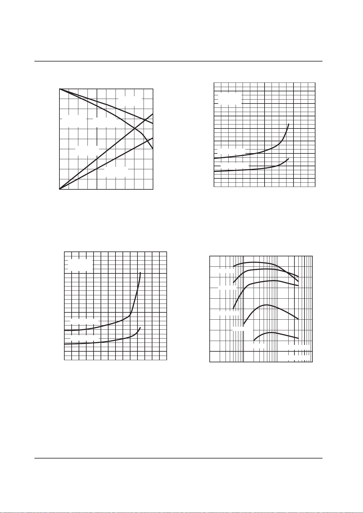
S1F76610 Series
100
90
×2 multiplier
Peff
80
Ta = 25°C
70
60
V
I
= –2.0V
×3 multiplier
Peff
50
Peff [%]
40
×3 multiplier
I
I
30
20
×2 multiplier
I
I
10
0
012345678910
I
O
[mA]
40
36
32
28
24
20
16
12
8
4
0
[mA]
I
I
Ta = 25°C
I
O
400
= 6mA
300
[Ω]
O
R
200
×3 multiplier
100
×2 multiplier
0
–7 –6 –5 –4 –3 –2 –1 0
V
I
[V]
(9) Multiplication efficiency/input current (10) Output impedance vs. Input voltage
vs. Output current
500
500
400
Ta = 25°C
I
O
= 10mA
100
IO = 2mA
90
I
O
= 5mA
300
[Ω]
O
R
200
×3 multiplier
100
×2 multiplier
0
–7 –6 –5 –4 –3 –2 –1 0
I
[V]
V
80
I
O
Peff [%]
70
= 10mA
I
O
= 20mA
60
I
O
= 30mA
50
1 10 100 1000
f
OSC
[kHz]
Ta = 25°C
VI = –5.0V
(11) Output impedance vs. Input voltage (12) Multiplication efficiency vs. Clock frequency
2–8 EPSON S1F70000 Series
Technical Manual
Page 52

S1F76610 Series
100
90
IO = 0.5mA
IO = 1.0mA
IO = 2.0mA
IO = 4.0mA
–7.850
VO = –15V
Ta = 25°C
–7.900
80
[V]
REG
Peff [%]
70
V
–7.950
Ta = 25°C
60
50
1 10 100 1000
OSC
[kHz]
f
VI = – 3.0V
–8.000
0.0001 0.0010 0.0100 0.1000
I
O
[V]
(13) Multiplication efficiency vs. Clock frequency (14) Output voltage vs. Output current
–5.850
VO = –9V
Ta = 25°C
–5.900
–2.850
VO = –6V
Ta = 25°C
–2.900
Series
S1F76610
[V]
REG
V
–5.950
–6.000
0.0001 0.0010 0.0100 0.1000
IO [V]
[V]
REG
V
–2.950
–3.000
0.0001 0.0010 0.0100 0.1000
I
O
[V]
(15) Output voltage vs. Output current (16) Output voltage vs. Output current
S1F70000 Series EPSON 2–9
Technical Manual
Page 53

S1F76610 Series
0.30
Ta = 25°C
0.25
0.20
0.15
|VREG-VO| [V]
0.10
0.05
0.00
0 5 10 15 20
I
O
[mA]
V
O
V
O
V
O
= –5V
= –10V
= –15V
50
(25°C)| [%]
REG
0
(25°C)|/|V
REG
(°C)|-|V
REG
100×|V
–50
–40 –20 0 20 40 60 80 100
Ta [°C]
(17) Regulator voltage vs. Output current (18) Regulator output stability ratio vs.
Ambient temperature
Temperature Gradient Control
The S1F7661C0B0 offers a choice of three temperature
gradients which can be used to adjust the voltage regulator output in applications such as power supplies for
driving LCDs.
POFF
1 (VDD)
1 (V
DD)
DD)
1 (V
1 (V
DD)
0 (VI)
0 (V
I)
I)
0 (V
I)
0 (V
TC2
See note 1.
O)
Low (V
Low (V
O)
High (V
High (V
DD)
DD)
Low (VO)
Low (V
O)
High (V
High (V
DD)
DD)
TC1
Low (V
High (V
Low (V
High (V
Low (VO)
High (V
Low (V
High (V
DD)
DD)
DD)
DD)
Temperature
See note 2.
O)
O)
O)
Notes
1. The definition of LOW for P
OFF differs from that for TC1 and TC2.
2. The temperature gradient affects the voltage between V
gradient
(%/˚C)
–0.4
–0.1
–0.6
–0.6
—
—
—
—
DD and VREG.
Voltage
regulator
output
ON
ON
ON
ON
OFF
(high impedance)
OFF
(high impedance)
OFF
(high impedance)
OFF
(high impedance)
CR osciliator
ON
ON
ON
OFF
OFF
OFF
OFF
OFF
Remarks
Serial connection
operational
CT0
CT1
CT2
Multiplier
2–10 EPSON S1F70000 Series
Technical Manual
Page 54
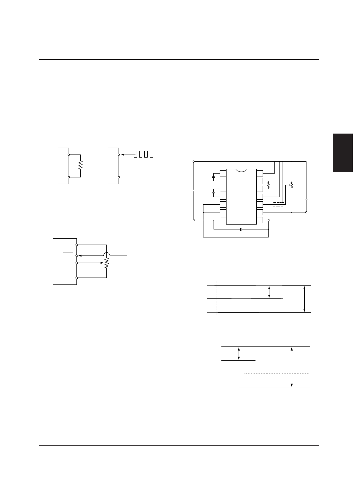
FUNCTIONAL DESCRIPTIONS
V
CC
(+5V)
GND
(–5V)
V
DD
= 0 V
V
I
= –5 V
V
CAP2
– = 2VI = –10 V
VDD = 0 V
V
I = –5 V
V
O = 3VI = –15 V
CR Oscillator
The on-chip CR oscillator network frequency is determined by the external resistor, R
tween OSC1 and OSC2. This oscillator can be disabled
in favor of an external clock by leaving OSC2 open and
applying an external clock signal to OSC1.
Oscillator External clock
OSC, connected be-
S1F76610 Series
Voltage Multiplier
The voltage multiplier uses the clock signal from the
oscillator to double or triple the input voltage. This requires three external capacitors–two charge-pump capacitors between CAP1+ and CAP1– and CAP2+ and
CAP2–, respectively, and a smoothing capacitor between V
I and VO.
OSC
OSC1
External clock
signal
OSC2
OSC1
R
OSC2
Reference Volatge Generator and Voltage
Regulator
The reference voltage generator supplies a reference
voltage to the voltage regulator to control the output.
This voltage can be switched ON and OFF.
V
DD
V
P
REG
OFF
RV
Control signal
R
RV
= 100 kΩ to 1 MΩ
VDD = 0 V
V
= –5 V
I
5 V
C1 +
10 µF
C2
10 µF
1
2
3
+
4
5
6
7
+
C3
10 µF
14
13
12
11
10
9
8
R
OSC
1 MΩ
VO = –15 V
Double voltage potential levels
R1
R2
R
RV
100 kΩ
to
1 MΩ
V
REG
C4
+
10 µF
= –8 V
Series
S1F76610
Tripled voltage potential levels
S1F70000 Series EPSON 2–11
Technical Manual
Page 55

S1F76610 Series
TYPICAL APPLICATIONS
Voltage Tripler with Regulator
The following figure shows the circuit required to triple
the input voltage, regulate the result and add a temperature gradient of –0.4%/°C. Note that the high input impedance of RV requires appropriate noise countermeasures.
VDD = 0 V
V
= –5 V
I
10 µF
5 V
10 µF
C1 +
C2
1
2
3
+
4
5
6
7
+
C3
10 µF
14
13
12
11
10
9
8
R1
R
OSC
1 MΩ
R2
VO = –15 V
R
RV
100 kΩ
to
1 MΩ
V
REG
C4
+
10 µF
= –8 V
R
RV
=V
R
1
RV
Converting a Voltage Tripler to a Voltage
Doubler
To convert this curcuit to a voltage doubler, remove capacitor C2 and short circuit CAP2– to V
VDD = 0 V
14
13
12
11
10
9
8
5 V
VI = –5 V
C1 +
10µF
C2
10µF
1
2
3
+
4
5
6
7
+
C3
10 µF
R
OSC
1 MΩ
O.
VO = –15 V
Parallel Connection
Connecting two or more chips in parallel reduces the
output impedance by 1/n, where n is the number of devices used.
Only the single output smoothing capacitor, C3, is re-
VDD = 0 V
14
13
12
11
10
R
OSC
1 MΩ
9
8
= –5 V
V
I
5 V
C1
10 µF
C2
10 µF
1
+
2
3
+
4
5
6
7
quired when any number of devices are connected in
parallel. Also, the voltage regulator in one chip is sufficient to regulate the combined output.
C1
10 µF
C2
10 µF
+
C3
10 µF
1
+
2
3
+
4
5
6
7
14
13
12
11
10
R
R
OSC
1 MΩ
9
8
V
= –15 V
O
RV
100 kΩ
to
1 MΩ
V
REG
+
C4
10 µF
= –10 V
2–12 EPSON S1F70000 Series
Technical Manual
Page 56

Serial Connection
Connecting two or more chips in series obtains a higher
output voltage than can be obtained using a parallel
<Precautions when connecting loads>
In case of series connections, when connecting loads
between the first stage V
second stage V
DD or up) and the second stage VREG as
shown in Fig. 2-13, be cautions about the following
point.
* When normal output is not occurring at the V
minal such as at times of starting up or when turning
the V
REG off by POFF signals, if current flows into the
second stage V
V
DD
= 0V
REG terminal through the load from
DD (or other potential of the
REG ter-
S1F76610 Series
connection, however, this also raises the output impedance.
the first stage VDD (or other potential of the second
stage V
absolute maximum rating for the second stage V
the V
hampered. Consequently, When making a series
connection, insert a diode D1 between the second
stage V
voltage exceeding the second stage V
not be applied to the V
DD or up) to cause a voltage exceeding the
DD at
REG terminal, normal operation of the IC may be
I and VREG as shown in Fig. 2-13 so that a
DD or up may
REG terminal.
V
DD'
= VI = –5V
Series
S1F76610
VI = –5V
5V
10µF
+
–
10µF
+–
14
1
13
2
3
4
5
6
7
12
11
10
9
VO = –10V= V
8
1MΩ
I
Positive Voltage Conversion
Adding diodes converts a negative voltage to a positive
one.
To convert the voltage tripler shown earlier to a voltage
doubler, remove C2 and D2, and short circuit D3. Small
Schottky diodes are recommended for all these diodes.
The resulting voltage is lowered by V
in the forward direction for each diode used. For example, if V
DD = 0V, VI = –5V, and VF = 0.6V, the re-
sulting voltages would be as follows.
• For a voltage tripler,
V
O = 10 – (3 × 0.6) = 8.2V
• For a voltage doubler,
V
O = 5 – (2 × 0.6) = 3.8V
F, the voltage drop
10µF
10µF
+
10µF
V
1
+
–
2
3
+
–
4
5
6
7
–
= 0 V
DD
5 V
VI = –5 V
D1
D2
D3
V
= 8.2 V
O
14
13
12
11
10
100kΩ
to
+
1MΩ
10µF
–
9
O
= –20V
V
8
D1
C1
+
C3
10 µF
10 µF
10 µF
+
C2
+
1
2
3
4
5
6
7
V
REG'
Load
= –15V
14
13
12
11
10
9
8
R
OSC
1 MΩ
S1F70000 Series EPSON 2–13
Technical Manual
Page 57
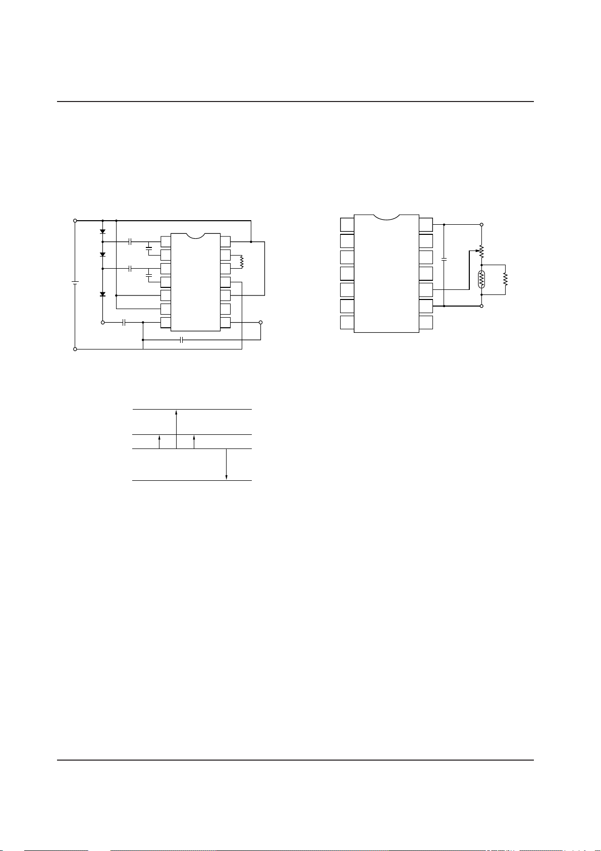
S1F76610 Series
Simultaneous Voltage Conversion
Combining a standard voltage tripler circuit with one
for positive voltage conversion generates both –15 and
8.2V outputs from a single input, however, it also raises
the output impedance.
A voltage doubler generates –10 and 3.8V outputs.
VDD = 0 V
= 8.2 V
O2
V
O2 = 8.2V
10 µF
+
10 µF
+
10 µF
10 µF
+
10 µF
1
2
++
3
4
5
6
7
+
10 µF
14
13
12
11
10
R
OSC
1 MΩ
9
V
= –15 V
O1
8
D1
D2
5 V
D3
V
= –5 V
V
I
Potential levels
Using an External Gradient
The S1F7661C0B0/M0B0 offers three built-in temperature gradients— –0.1, –0.4 and –0.6%/°C.
To set the gradient externally, place a thermistor, R
series with the variable resistor, R
RV, used to adjust the
output voltage.
R1
V
R
V
1
2
3
4
5
6
7
14
13
12
11
10
9
8
+
10 µF
T, in
DD
RV
R
R
T
P
REG
VDD = 0 V
I = –5 V
V
O1 = –15 V
V
2–14 EPSON S1F70000 Series
Technical Manual
Page 58

S1F76540 Series
S1F76540 Series Charge Pumping DC/DC Converter &
Voltage Regulator
DESCRIPTION
The S1F76540C0A0/M0A0 is a CMOS process,
charge-pumping DC/DC converter and voltage regulator featuring the very high efficiency but low power
consumption. An addition of four, three, or two external capacitors can generate four-, three- or two-time
output voltage in negative direction than the input voltage. Also, the built-in voltage regulator can set any output voltage of DC/DC converter and can output the
regulated voltage using two external resistances. As the
regulator output can have a negative temperature gradient that is required for LCD panels, it is optimum for the
LCD panel power supply.
FEATURES
• Charge-pumping, DC-to-DC converter (four-, threeor two-time negative boosting)
• Built-in voltage regulator (regulated voltage output
circuit)
• High power conversion
efficiency : 95%
• Low current consumption : 130 µA (V
during four-time
boosting, Typ.)
• High output capacity : 20 mA (Max.)
I = –5.0 V
• Input voltages : –2.4 to –5.5 V (during
four-time boosting)
: 2.4 to –7.3 V (during
three-time boosting)
: 2.4 to –11 V (during
two-time boosting)
• DC/DC converter output
voltage : |Input voltage| × 4
(Max.)
• Built-in reference voltage for
high-precision regulator : 1.5 ± 0.05 V (at C
• Temperature gradient
function of regulator
output voltages : – 0.04, – 0.15, – 0.35,
– 0.55 (%/°C)
• Low standby current
(during power-off) : 5.0 µA
• Power-off by the external signal
• Full built-in oscillator circuit
• Lineup : S1F76540M0A0,
16-pin SSOP
: S1F76540C0A0,
16-pin DIP
T0)
APPLICATIONS
• Power supply of medium- and small-capacity LCD
panels
• Regulated power supply of battery driven devices
Series
S1F76540
S1F70000 Series EPSON 2–15
Technical Manual
Page 59
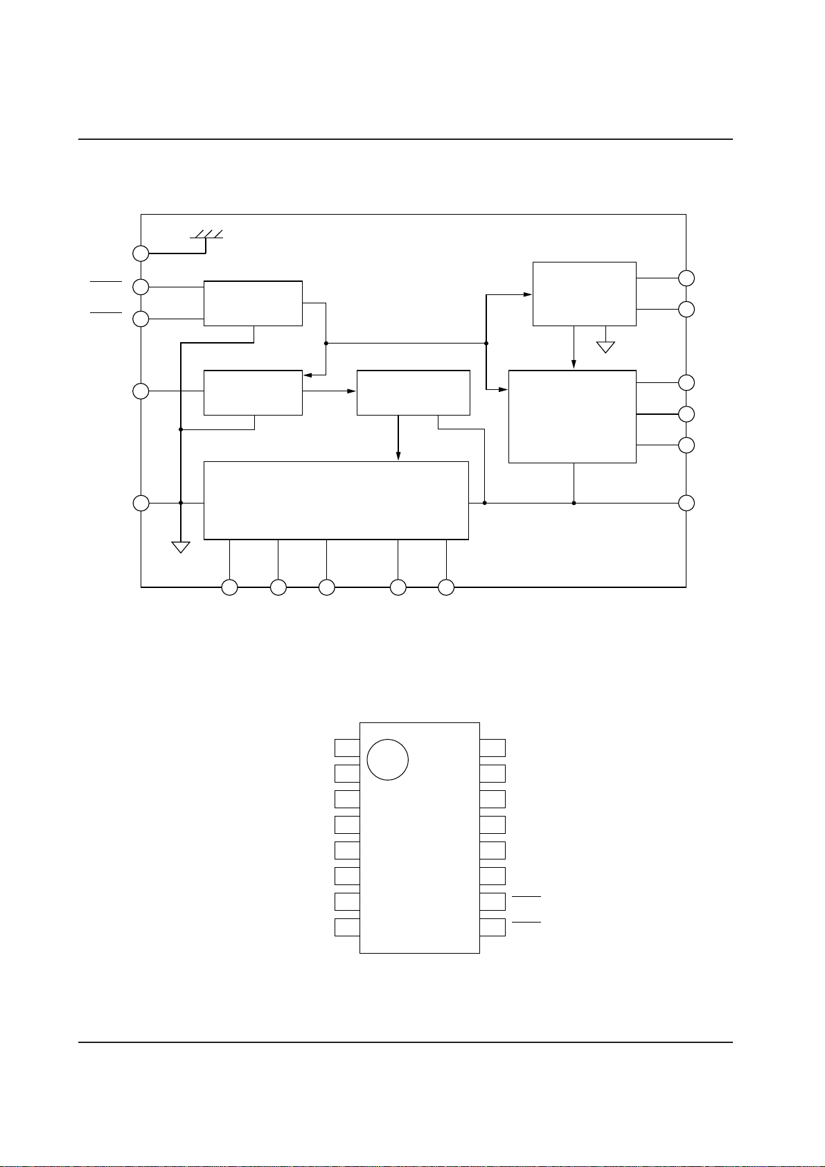
S1F76540 Series
BLOCK DIAGRAM
V
DD
P
P
OFF1
OFF2
FC
V
Power-off
control circuit
Clock
generator
circuit
Booster control
circuit
Reference
voltage
circuit
Voltage
regulation
TC1
TC2
RV
V
REG
circuit
V
RI
I
Voltage converter
circuit
O
V
C1P C2NC2PC3NC1N
Figure 2.1 Block diagram
PIN DESCRIPTIONS
V
1
O
2
VRI
RV
V
DD
FC
TC1
TC2
3
4
5
6
7
8
VREG
Figure 2.2 S1F76540M0A0/C0A0 pin assignments
2–16 EPSON S1F70000 Series
16
15
14
13
12
11
10
C2P
C2N
C3N
C1N
C1P
V
I
POFF1
9
POFF2
Technical Manual
Page 60

Table 2.1 Pin descriptions
Pin name Pin No. Pad No. Description
VO 1 18 Four-time booster output
VRI 2 19 Regulator input
VREG 3 20 Regulator output
RV 4 21 Regulator output voltage adjustment input
VDD 5 22, 23 Power pin (positive)
S1F76540 Series
FC 6 24 Internal clock frequency input, and clock input in serial/parallel
connection
TC1 7 3 Regulator output temperature gradient setup input (1)
TC2 8 4 Regulator output temperature gradient setup input (2)
POFF2 9 5 Power-off control input (2)
POFF1 10 6 Power-off control input (1)
VI 11 11, 12 Power voltage (negative)
C1P 12 13 Two- or four-time booster capacitor positive pin
C1N 13 14 Two-time booster capacitor negative pin
C3N 14 15 Four-time booster capacitor negative pin
C2N 15 16 Three-time booster capacitor negative pin
C2P 16 17 Three-time booster capacitor positive pin
Series
S1F76540
S1F70000 Series EPSON 2–17
Technical Manual
Page 61

S1F76540 Series
Table 2.2 Absolute maximum ratings
Parameter Symbol Rating Unit Remarks
Min. Max.
V
DD reference
Input power voltage V
Input pin voltage V
I
1
Output pin voltage 1 VOC1 VI
–26.0/N VDD + 0.3 V
VI – 0.3 VDD + 0.3 V
–
Output pin voltage 2 VOC2 2 × VI
Output pin voltage 3 VOC3 3 × VI
Output pin voltage 4 VOC4 4 × VI
Regulator input power
voltage
Regulator input pin voltage
Output voltage V
V
RI
N × VI – 0.3 VDD + 0.3 V
VRV N × VI – 0.3 VDD
N × VI – 0.3 VDD + 0.3 V
O
0.3 V
0.3 V
–
– 0.3 2 × V
– 0.3 3 × V
DD
0.3 V C1P and C2P pins
+
I
0.3 V C1N pin
+
I
+ 0.3 V C2N pin
I
+ 0.3 V C3N pin
+ 0.3 V
N = Boost time
V
I pin
OFF1, POFF2, TC1,
P
TC2 and FC pins
N = Boost time, VRI pin
N = Boost time, RV pin
N = Boost time
V
O and VREG pins
Input current II 80 mA VI pin
Output current I
O
N ≤ 4: 20
N > 4: 80/N V
mA
N = Boost time
O and VREG pins
Allowable loss PD 210 mW Ta ≤ 25°C
Operating temperature Topr –30 85 °C
Storage temperature Tstg –55 150 °C
Soldering temperature
and time
Tsol 260
•
10 °C • s At leads
Notes: 1. An operation exceeding the above absolute maximum ratings may cause a malfunction or
permanent damage of devices. The device reliability may drop excessively even if the devices
temporarily operate normally.
2. Electrical potential to peripheral systems:
The S1F76540 common power supply has the highest potential (V
tial given by this specification is based on V
DD = 0 V. Take care to avoid a potential problem
DD). The electrical poten-
during connection to a peripheral system.
2–18 EPSON S1F70000 Series
Technical Manual
Page 62

Figure 2.3 Potential relationship
S1F76540 Series
V
(+5 V)
GND
(0 V)
System S1F76540
CC
5 V
Two-time
boosting
ELECTRICAL CHARACTERISTICS
Table 2.3 DC characteristics (1)
Parameter Symbol Characteristics Min. Typ. Max. Unit
10 V
15 V
Three-time
boosting
V
DD
(0 V)
I
V
(–5 V)
–10 V
–15 V
20 V
–20 V
Four-time
boosting
Ta = –30°C to +85°C, V
DD = 0 V, VI = –5.0 V
unless otherwise noted
Series
S1F76540
N = Boost time if CT0 is selected –22/N –2.4 V
Input power voltage VI
N = Boost time if CT1 is selected –22/N –2.4 V
N = Boost time if CT2 is selected –22/N –2.4 V
N = Boost time if CT3 is selected –22/N –2.4 V
Boost start input power
voltage no loading
V
STA
N = Boost time, FC = VDD during
–22/N –2.4 V
Boost output voltage VO –22 V
Regulator input voltage VRI –22 –2.4 V
Regulator output voltage VREG
S1F70000 Series EPSON 2–19
Technical Manual
IREG = 0, VRI = –22 V
R
RV = 1MΩ
–2.4 V
Page 63

S1F76540 Series
Table 2.3 DC characteristics (2)
Parameter Symbol Characteristics Min. Typ. Max. Unit
Boost output impedance R
Boost power conversion
efficiency
Peff
IO = 10 mA, VI = –5.0 V during
4-time boosting
C1, C2, C3, CO = 10 µF (tantalum)
O
IO = 10 mA, VI = –3.0 V,
Ta = 25°C during 4-time boosting
C1, C2, C3, CO = 10 µF (tantalum)
IO = 2 mA, VI = –5.0 V during
4-time boosting
C1, C2, C3, CO = 10 µF (tantalum)
IO = 2 mA, VI = –3.0 V, Ta = 25°C
during 4-time boosting
C1, C2, C3, CO = 10 µF (tantalum)
Ta = –30°C to +85°C, V
DD = 0 V, VI = –5.0 V
unless otherwise noted
200 300 Ω
250 300 Ω
95 %
94 %
FC = VDD, P
V
I
= –5.0 V during no loading
Booster operation current
consumption 1
OPR1
I
C1, C2, C3, CO = 10 µF (tantalum)
FC = VDD, POFF1 = VI, POFF2 = VDD,
V
I = –3.0 V, Ta = 25°C during no loading
C1, C2, C3, CO = 10 µF (tantalum)
FC = VI, P
V
I
= –5.0 V during no loading
Booster operation current
consumption 2
OPR2
I
C1, C2, C3, CO = 10 µF (tantalum)
FC = VI, POFF1 = VI, POFF2 = VDD,
V
I = –3.0 V, Ta = 25°C during no loading
C1, C2, C3, CO = 10 µF (tantalum)
Regulator operation
current consumption no loading
I
OPVR
Static current I
Input leakage current I
Regulated output
saturation resistance
LKI
SAT (*1) RV = VDD 10 20 Ω
R
VRI = –20 V, RRV = 1 MΩ during
POFF1 = VI, POFF2 = VI
Q
FC = V
DD
Pins used: POFF1, POFF2, FC,
TC1, TC2
REG < 20 mA
0 < I
Ta = 25°C
OFF1
OFF1
= VI, P
= VI, P
OFF2
OFF2
= VDD,
130 220 µA
100 150 µA
= VDD,
520 880 µA
400 600 µA
10 15 µA
5.0 µA
0.5 µA
Regulated output
voltage stability
–20 V < V
∆V
R (*2) VREG = –9 V 0.2 %/V
Ta = 25°C
RI < –10 V, IREG = 1 mA
2–20 EPSON S1F70000 Series
Technical Manual
Page 64

Table 2.3 DC characteristics (3)
Parameter Symbol Characteristics Min. Typ. Max. Unit
Regulated output load
variation
O (*3) Ta = 25°C setup 30 50 mV
∆V
VREF0 TC1 = VDD, TC2 = VDD –1.55 –1.50 –1.45 V
V
Reference voltage
(Ta = 25°C)
REF1 TC1 = VDD, TC2 = VI –1.70 –1.50 –1.30 V
REF2 TC1 = VI, TC2 = VDD –1.90 –1.50 –1.10 V
V
VREF3 TC1 = VI, TC2 = VI –2.15 –1.50 –0.85 V
C
Reference voltage
temperature coefficient
(*4, *5)
C
C
CT3
RI = –20 V, VREG = –15 V,
V
0 < I
REG < 20 mA
T0
TC1 = VDD, TC2 = VDD, SSOP product
T1
TC1 = VDD, TC2 = VI, SSOP product
T2
TC1 = VI, TC2 = VDD, SSOP product
TC1 = VI, TC2 = VI, SSOP product
Ta = –30°C to +85°C, V
–0.07 –0.04 0 %/°C
–0.25 –0.15 –0.07 %/°C
–0.45 –0.35 –0.20 %/°C
–0.75 –0.55 –0.30 %/°C
S1F76540 Series
DD = 0 V, VI = –5.0 V
unless otherwise noted
Series
S1F76540
VI = –2.4 to –5.5 V
V
Input voltage level
IH Pins used: POFF1, POFF2, FC,
TC1, TC2
0.2 V
I
V
VI = –2.4 to –5.5 V
V
IL Pins used: POFF1, POFF2, FC,
0.8 VIV
TC1, TC2
Booster capacitance CMAX Capacitors used: C1, C2 and C3 47 µF
REG – VRI)
*1 RSAT =
*2 ∆VR =
*3 ∆VO =
*4 CT =
∆ (V
REG
∆I
REG (VRI = –20 V) – VREG (VRI = –10 V)
V
RI • VREG (VRI = –10 V)
∆V
REG (IREG = 20 mA) – VREG (IREG = 0 mA)
V
REG
∆I
REF (50°C) | – | VREF (0°C) |
| V
50°C – 0°C| V
×
100
REF (25°C) |
*5 The reference voltage and temperature coefficient of the chip products may vary depending on the mold-
ings used on each chip. Use these chips only after the temperature test.
S1F70000 Series EPSON 2–21
Technical Manual
Page 65
S1F76540 Series
Table 2.4 AC characteristics
Parameter Symbol Conditions Min. Typ. Max. Unit
V
DD = 0 V and VI = –5.0 V
unless otherwise noted
FC = VDD,
Internal clock frequency 1 f
CL1
POFF1 = VI
P
= V
OFF2
Pin used: C1P to +85°C
FC = VI,
Internal clock frequency 2 f
CL2
POFF1 = VI
P
= V
OFF2
Pin used: C1P to +85°C
FUNCTIONAL DESCRIPTIONS
Clock Generator Circuit
As the S1F76540 has a built-in clock generator circuit,
no more parts are required for voltage boost control.
The clock frequency changes according to the FC pin
voltage level as defined on Table 2.5. Low Output mode
or High Output mode is selectable. This allows frequency selection according to the used capacitance and
Table 2.5 FC pin setup
Ta = 25°C 3.0 4.0 6.0 kHz
DD
Ta = –30°C
2.0 4.0 7.0 kHz
Ta = 25°C 12.0 16.0 24.0 kHz
DD
Ta = –30°C
8.0 16.0 28.0 kHz
load current as the boost output impedance changes depending on the clock frequency and external booster capacitance. However, the High Output mode has the
current consumption approximately four times larger
than the Low Output mode.
Characteristics
FC pin Mode
High (VDD) Low Output 4.0 kHz (Typ.) IOP (*1) VRR (*2)
Low (VI) High Output 16.0 kHz (Typ.)
Clock frequency Current Output ripple
consumption
IOP × Approx. 4
VRI × Approx. 1/4
Output Capacitance
impedance
See Figure A1. See Figure A1.
See Figure A1. See Figure A1.
*1 See the DC characteristics table for current consumption.
*2 See Section Page 2-32 for the output ripple definition and calculation.
2–22 EPSON S1F70000 Series
Technical Manual
Page 66

S1F76540 Series
Capacitance vs. output impedance characteristic when 4X pressure is applied
Load current = 10 mA, Ta = 25°C, C1 = C2 = C
Capacitor used: Tantalum electrolytic capacitor
550
500
450
400
350
Output impedance [Ω]
300
0
Series
S1F76540
250
200
150
110
100
C [µF]
I = –3.0V FC = High
V
VI = –5.0V FC = High
VI = –3.0V FC = Low
VI = –5.0V FC = Low
Figure A1 Characteristic chart: Capacitance vs. output impedance when 4X pressure is applied
NOTE: This characteristic chart simply indicates an approximate trend in the characteristics, which
may vary depending on evaluation environment, parts used, and other factors.
S1F70000 Series EPSON 2–23
Technical Manual
Page 67

S1F76540 Series
Voltage Converter
The voltage converter, consisting of a boost control circuit and a voltage converter circuit, receives clocks
from the clock generator circuit and boosts the input
power voltage (V
I) four, three or two times. During
four-time boosting, however, the three-time and two-
Figure 2.4 Electrical potentials during boosting (at –5V input)
10 V
Two-time
boosting
time boost outputs cannot be obtained simultaneously.
Figure 2.4 gives the potential relationship during four-,
three- and two-time boosting. The C2P pin is also used
as the master clock output during parallel connection.
15 V
V
DD
(0 V)
I
V
(–5 V)
–10 V
–15 V
Three-time
boosting
20 V
–20 V
Four-time
boosting
Caution:
• When connecting a capacitor to the C1P, C2P, C1N, C2N, C3N, or V
O pin for voltage conversion,
close the capacitor to the IC package as much as possible to minimize the wiring length.
2–24 EPSON S1F70000 Series
Technical Manual
Page 68

Reference Voltage Circuit
The S1F76540 has a built-in reference voltage circuit
for voltage regulation. The regulated voltage (explained in the next “voltage regulator circuit” section) is
set depending on the division ratio between this refer-
Table 2.6 Setup of reference voltage and temperature coefficient
TC1 TC2 Reference voltage, Temperature coefficient,
(High = V
DD) (High = VDD)VREF (V) CT (%/°C)
ence voltage and the external resistance. The reference
voltage can be used to change the temperature coefficient at pins TC1 and TC2. One of four states can be
selected as listed on Table 2.6.
S1F76540 Series
Mode (Low = VI) (Low = VI) Min. Typ. Max. Min. Typ. Max.
CT0 High High –1.55 –1.5 –1.45 –0.07 –0.04 0
CT1 High Low –1.70 –1.5 –1.30 –0.25 –0.15 –0.07
CT2 Low High –1.90 –1.5 –1.10 –0.45 –0.35 –0.20
CT3 Low Low –2.15 –1.5 –0.85 –0.75 –0.55 –0.30
Notes: 1. The reference voltage is given at Ta = 25°C.
2. The reference voltage and temperature coefficient of the chip products may vary depending
on the moldings used on each chip. Use these chips only after the temperature test.
The temperature coefficient (C
cient (C
T) means that the |VREF| value decreases when the temperature rises.
CT =
T) is defined by the following equation. The negative sign of the temperature coeffi-
REF (50°C) | – | VREF (0°C) |
| V
50°C – 0°C| V
×
100
REF (25°C) |
Notes on TC1 and TC2 pin replacement:
• When replacing the TC1 and TC2 pins after power-on, always select the power-off mode (P
OFF1 = POFF2 = VI)
and replace them by each other.
Voltage Regulator Circuit
The voltage regulator circuit regulates a voltage entered
in the V
RI pin and can output any voltage. It uses the
series voltage regulation. As shown in Figure 2.5, the
V
RI and VO pins must be short-circuited by a jumper as
short as possible except for larger time boosting by using external diodes.
As shown by equation (1), any output voltage can be set
by the ratio of external division resistors R1 and R2.
The sum of division resistance is recommended to be
small as possible to avoid an external noise interference. As the current consumed by division resistors
(equation (2)) flows, the 100Ω to 1MΩ are recommended to use.
The temperature coefficient of the regulated voltage is
equal to the temperature coefficient of the reference
voltage that is explained in the “reference voltage circuit” section.
Series
S1F76540
S1F70000 Series EPSON 2–25
Technical Manual
Page 69

S1F76540 Series
R1
Figure 2.5 V
Setup:
• Relationship between V
VREG =
R1 + R2
REG and reference voltage
× (Reference voltage) • • • • Equation (1)
R1
• Current consumption of division resistors
REG |
IREG =
| V
R1 + R2
P
P
C2P
C2N
C3N
C1N
C1P
OFF1
OFF2
16
15
14
13
12
V
I
11
10
9
V
O
1
V
RI
R2
REG setup and mounting notes
2
V
REG
3
RV
4
V
DD
5
FC
6
TC1
7
TC2
8
• • • • Equation (2)
Setup example:
• To output V
REG = –18 V by four-time boosting if VI = –5 V and VO = –20 V
First, determine the total resistance of division resistors R1 and R2. If the current consumption is assumed to be 20
µA, the total resistance can be obtained from equation (2) as follows:
R1 + R2 = 12V ÷ 20 µA = 900 kΩ
If the reference voltage is -1.5 V, the division resistance ratio can be obtained from equation (1) as follows:
(R1 + R2) / R2 = (–18 V) ÷ (–1.5 V) = 12
Therefore, R1 and R2 are:
R1 = 75 kΩ
R2 = 825 kΩ
2–26 EPSON S1F70000 Series
Technical Manual
Page 70

S1F76540 Series
Changing the temperature coefficient:
• The temperature coefficient of the regulated voltage depends on the temperature coefficient of the reference
voltage (if the division ratio of setup resistors does not depend on the temperature). It is necessary to change the
temperature coefficient using thermistors, resistors or others to set any other temperature coefficient of the
regulated voltage. The following explains how to calculate the V
TR2 × R2 (T0)
REG (T) = 1 +
V
0 :25°C
T
C
TR1 : Temperature coefficient of resistor R1 (Ratio to the value at 25°C)
C
TR2 : Temperature coefficient of resistor R2 (Ratio to the value at 25°C)
C
T : Temperature coefficient of internal reference voltage (%/°C)
R1 (T
0) : R1 value (Ω) at 25°C
R2 (T
0) : R2 value (Ω) at 25°C
V
REF (T0) : Internal reference voltage (V) at 25°C
C
{} ][
C
TR1 × R1 (T0) 100
× 1+ (T – T
T
C
) ×
0
REG voltage in temperature T.
• • • • Equation (3)
Series
S1F76540
If the temperature coefficient of R1 and R2 is identical in equation (3), the V
REG voltage depends on the tem-
perature coefficient of internal reference voltage only.
Application notes on voltage regulator circuit:
• To satisfy the absolute maximum ratings of the S1F76540, the setup resistor(s) must be inserted between V
and VREG pins of the S1F76540 that uses the voltage regulator. The S1F76540 IC itself may be degraded or
destroyed if the R1 resistor is connected to pin V
DD of S1F76540 that does not use the regulator during serial
connection.
• The regulation voltage adjustment input (pin RV) has the very high input impedance, and its noise insertion can
drop the regulator stability. As shown in Figure 2.5, shield the cable between the division resistor and RV pin or
use a cable as short as possible between them.
DD
S1F70000 Series EPSON 2–27
Technical Manual
Page 71

S1F76540 Series
Power-off Control Function
The S1F76540 has the power-off function and turns on
or off each circuit function when control signals are entered in the P
OFF1 and POFF2 pins from an external sys-
tem (such as microprocessor) as defined on Table 2.7.
This power-off function can also cut the reactive current
Table 2.7 Available combination of power-off control
POFF1 POFF2 Functions
in parallel connection and other application circuits.
To use the dual-state, power-off control (all ON and all
OFF states) only, connect pin P
only pin P
OFF2 to pin VI and use
OFF1 for power-off control.
Mode
(High = VDD) (High = VDD)
(Low = VI) (Low = VI)
Oscillator Booster Regulator Applications
circuit circuit
PS1 High Low ON ON ON All circuits are turned on.
PS2 Low Low OFF OFF (*1) OFF (*2) All circuits are turned off.
PS3 High High OFF ON ON
PS4 Low High ON ON OFF
Slave unit side of parallel connection
(Booster and regulator)
Master unit side of parallel
connection (Booster only)
*1 When the booster circuit is off, approximately VI + 0.6 V voltage appears at VO pin.
*2 When the regulator is off, the V
REG pin becomes high-impedance state.
Application notes on power-off function:
• When using external system signals for power-on control, start to control the power only when V
becomes stable after power-on. Unstable V
V
I
I voltage may destroy the IC permanently during on/off control.
V
I
I voltage
P
P
OFF1
OFF2
P
P
OFF1
OFF2
Figure 2.6 Start timing of power-off control
2–28 EPSON S1F70000 Series
Technical Manual
Page 72

CHARACTERISTICS GRAPH
S1F76540 Series
200
180
160
140
120
100
Booster current consumption [µA]
80
60
40
0
621
Input voltage [V]
Input voltage (VI) vs. Booster circuit current consumption (I
V
O
(V)
V
I
= –3 V, Four-times Booster VI = –5 V, Four-times Booster
P
(%)
OPR
eff
300
280
260
240
220
200
180
Booster output impedance [Ω]
160
140
120
100
12345675473
)
Input voltage (V
V
O
(V)
Input voltage [V]
I
) vs. Booster output impedance (RO)
P
(%)
Series
S1F76540
eff
–12.00
0
0
O
(mA) IO (mA)
I
20.00
Power conversion efficiency (Peff) vs. Output voltage (VO)
Input current (I
O
) vs. Output voltage (VO)
Figure 2.7 Characteristics graphs
100.0
–20.00
V
O
P
eff
50.00
0 50.00
0 20.00
Power conversion efficiency (Peff) vs. Output voltage (V
Input current (I
O
) vs. Output voltage (VO)
100.0
V
O
P
eff
O
)
S1F70000 Series EPSON 2–29
Technical Manual
Page 73

S1F76540 Series
APPLICATION CIRCUIT EXAMPLES
Four-time Booster and Regulator
Figure 2.8 gives a wiring example of four-time booster
and regulator that is the typical S1F76540 application.
This example boosts the input voltage (V
V
REG
V
DD
V
I
Figure 2.8 Wiring example of 4-time booster and regulator
I) four times in
C
O
+
C
REG
+
R1
R2
+
C
I
negative direction, and outputs the regulated voltage at
V
REG pin.
V
O
1
2
V
RI
3
V
REG
4
RV
5
V
DD
FC
6
TC1
7
TC2
8
P
P
C2P
C2N
C3N
C1N
C1P
OFF1
OFF2
16
15
14
13
12
V
I
11
C1
+
C2
C3
+
+
10
9
◊
Setup conditions of Figure 2.8
• Internal clock : ON (Low Output mode)
• Booster circuit : ON
• Regulator : ON (if C
◊
Power-off procedure
• Set the P
◊
Regulator
OFF1 pin to logical low (VI) to turn off all circuits.
T = –0.04%/°C)
• For the regulator setup and notes, see the “voltage regulator circuit” section.
◊
Application in other setup conditions
1 When used in the High Output mode
• Connect the FC pin to the V
2 When changing the temperature coefficient (C
I pin.
T)
• Change the TC1 and TC2 pin setup by following the definition of Table 2.7.
2–30 EPSON S1F70000 Series
Technical Manual
Page 74

4-time Booster
Only the booster circuit operates, and it boosts the input
voltage (V
it at the V
I) four times in negative direction and outputs
O pin. As the regulator is not used, the voltage
C
O
+
V
O
V
DD
appearing at the V
O pin may contain ripple components.
Figure 2.9 gives a wiring example.
16
V
O
1
V
RI
2
V
REG
3
RV
4
DD
V
5
C2P
C2N
C3N
C1N
C1P
15
14
13
12
+
C2
C1
+
S1F76540 Series
C3
+
Series
S1F76540
P
P
OFF1
OFF2
11
V
I
10
9
FC
6
+
I
C
V
I
TC1
7
TC2
8
Figure 2.9 Wiring example of 4-time booster
◊
Setup conditions of Figure 2.9
• Internal clock : ON (Low Output mode)
• Booster circuit : ON
• Regulator : OFF
◊
Power-off procedure
• Set the P
◊
Ripple voltage
• As the output at V
(V
OFF2 pin to low (VI) to turn off all circuits.
O pin is unstable, it can contain ripple components as shown in Figure 2.10. The ripple voltage
RP) increases according to the load current, and it can roughly be calculated by equation (4).
S1F70000 Series EPSON 2–31
Technical Manual
Page 75

S1F76540 Series
O
VRP =
2 • f
I
CL • CO
+ IO • RCOUT • • • • Equation (4)
where,
I
O : Load current (A)
f
CL : Clock frequency (Hz)
R
COUT : Serial equivalent resistance (Ω) of output capacitor CO
Figure 2.10 Ripple waveforms
◊
Application in other setup conditions
1 When used in the High Output mode
Connect the FC pin to the V
I pin.
Parallel Connection (for Increased Boosting)
The parallel connection is useful for reduction of
booster output impedance or reduction of ripple voltage. In the parallel connection of “n” lines, the booster
output impedance can be reduced to approximately “1/
n". Only the smoothing capacitor (C
put can be used commonly in the parallel connection.
When using the regulator, use only one of “n”
O) for booster out-
V
RP
S1F76540 chips which are in parallel connection. (If
multiple regulators are operated in parallel mode, the
reactive current consumption occurs.) Figure 2.11
gives a wiring example of 4-time booster and regulator
where two S1F76540s are parallelly connected.
V
REG
+
O
C
V
DD
+
C
I
V
I
1
2
3
4
5
6
7
8
VO
VRI
VREG
RV
DD
V
FC
TC1
TC2
C2P
C2N
C3N
C1N
C1P
POFF1
POFF2
16
+
15
C2
14
13
12
11
V
I
10
9
C1
C3
+
+
R1
C
REG
+
R2
VO
1
VRI
2
3
VREG
4
RV
5
DD
V
6
FC
7
TC1
8
TC2
C2P
C2N
C3N
C1N
C1P
POFF1
POFF2
V
I
+
16
15
C2
14
13
12
11
10
9
C1
C3
+
+
Figure 2.11 Parallel connection example
2–32 EPSON S1F70000 Series
Technical Manual
Page 76
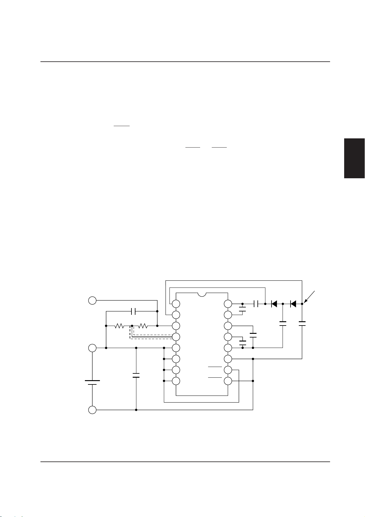
S1F76540 Series
◊
Setup conditions of Figure 2.11
First stage Second stage
• Internal clock : ON (Low Output mode) • Internal clock : OFF
• Booster circuit : ON • Booster circuit : ON
• Regulator : OFF • Regulator : ON (if C
◊
Power-off procedure
• In Figure 2.11, when the P
OFF2 pin of the first-stage S1F76540 is set to low (VI), voltage boosting is stopped at
the first and second stages. However, the regulator at the second stage does not stop. Therefore, the voltage that
is approximately V
• To set the V
I appears at VREG pin during |VREG| > |VI| setup.
REG pin to high-impedance state, set both POFF1 and POFF2 pins to low at the first and second stages.
T = –0.04%/°C)
◊
Application in other setup conditions
1 When used in the High Output mode
• Connect the FC pin of the first-stage S1F76540 to the V
2 When changing the temperature coefficient (C
T)
I pin.
• Change the TC1 and TC2 pin setup by following the definition of Table 2.7.
Larger Time Boosting Using Diodes
The S1F76540 can be configured to have the five-time
or larger voltage boosting and regulation by adding external diodes. As the booster output impedance increases due to the diode forward voltage drop (V
diodes having a smaller V
V
REG
V
DD
F are recommended to use.
C
REG
+
R1
R2
F), the
Figure 2.12 gives a wiring example of 6-time booster
and regulator that use two diodes. The wiring between
O and VRI must be minimal. Figure 2.13 provides the
V
potential relationship.
O
1
V
V
RI
2
V
REG
3
RV
4
V
DD
5
FC
6
C2P
C2N
C3N
C1N
C1P
V
Series
S1F76540
VO'
C4
+
16
15
14
13
12
11
I
C1
+
C2
C3
+
+
D2D1
C5
O
C
++
TC1
+
C
I
V
I
7
TC2
8
P
P
OFF1
OFF2
10
9
Figure 2.12 Wiring example for 6-time boosting using diodes
S1F70000 Series EPSON 2–33
Technical Manual
Page 77

S1F76540 Series
◊
Setup conditions of Figure 2.12
• Internal clock : ON (Low Output mode)
• Booster circuit : ON
• Regulator : ON (if C
Figure 2.13 Potential relationship during 6-time boosting using diodes
T = –0.04%/°C)
V
DD
V
I
V
O
4V
V
I
I
6V
I
2∗V
F
6VI – (2∗VF)
V
O
'
◊
Power-off procedure
• Set the P
◊
Output voltages
OFF1 pin to low (VI) to turn off all circuits.
• When diodes are used for voltage boosting, the characteristics of diodes directly affect on the voltage boosting
characteristics. The forward voltage drop (V
of Figure 2.12 uses two diodes, the drop of “V
F) of diodes can reduce the booster output voltage. As the example
F” voltage multiplied by two occurs as shown in Figure 2.13. The
booster output voltage is expressed by equation (5).
To increase the |V
| V
O' | = 6 × | VI | – 2 × VF • • • • Equation (5)
◊
Notes
O'| value, use the diodes having a smaller VF.
1 Input and output current conditions
To satisfy the input and output current ratings, limit the total current does not exceed the rated input current.
The total current means the total boost time multiplied by the output load current. The example of Figure 2.12
has the maximum load current of 13.3 mA ( = 80 mA divided by 6).
2 Input and output voltage conditions
To satisfy the input and output voltage ratings, take care not to violate the electric potential relationship of
higher time boosting using diodes. The example of Figure 2.12 must have the “V
I” that can satisfy the input
voltage conditions during 6-time boosting (see Table 2.3).
◊
Application in other setup conditions
1 When used in the High Output mode
Connect the FC pin to the V
2 When changing the temperature coefficient (C
I pin.
T)
Change the TC1 and TC2 pin setup by following the definition of Table 2.7.
2–34 EPSON S1F70000 Series
Technical Manual
Page 78

Positive Voltage Conversion
The S1F76540 can also boost up a voltage to the positive potential using external diodes. In such case, however, the regulator function is unavailable. Figure 2.14
1
2
3
4
V
DD
5
6
S1F76540 Series
gives a wiring example for three-time positive boosting,
and Figure 2.15 provides its electrical potential relationship.
V
V
V
RV
V
FC
O
RI
REG
DD
D1
C2P
C2N
C3N
C1N
C1P
V
16
15
14
13
12
I
11
C1
D2 D3
+
+
C2
VO'
+
O
C
Series
S1F76540
+
C
I
V
I
TC1
7
TC2
8
P
P
OFF1
OFF2
10
9
Figure 2.14 Wiring example of positive voltage conversion (3-time boosting)
◊
Setup conditions of Figure 2.14
• Internal clock : ON (Low Output mode)
• Booster circuit : ON
• Regulator : OFF
F
3∗V
3VI
VDD
VO'
3VI – (3∗VF)
VI
VI
Figure 2.15 Potential relationship during positive voltage conversion (3-time boosting)
◊
Power-off procedure
• Set the P
◊
Two-time boosting
OFF2 pin to low (VI) to turn off all circuits.
• To boost up a voltage two times, remove capacitor C1 and diode D1 of Figure 2.14, and connect the anode of
diode D2 to the V
S1F70000 Series EPSON 2–35
Technical Manual
DD pin.
Page 79

S1F76540 Series
◊
Output voltages
• When diodes are used for voltage boosting, the characteristics of diodes directly affect on the voltage boosting
characteristics. The forward voltage drop (V
of Figure 2.14 uses three diodes, the drop of “V
F) of diodes can reduce the booster output voltage. As the example
F” voltage multiplied by three occurs. The booster output
voltage is expressed by equation (5).
To increase the |V
| V
O' | = 3 × | VI | – (3 × VF) • • • • Equation (6)
◊
Notes
O'| value, use the diodes having a smaller VF.
1 Input and output current conditions
To satisfy the input and output current ratings, take care to limit the input current below the ratings.
2 Input and output voltage conditions
During forward voltage conversion, the input voltage ratings are the same as two-time negative voltage boosting (see Table 2.3).
◊
Application in other setup conditions
When used in the High Output mode, connect the FC pin to the V
I pin.
Wiring Example When Changing the
Regulator Temperature Coefficient
The temperature coefficient of the regulator depends on
the temperature coefficient of the internal reference
voltage. To set another temperature coefficient, use a
thermistor resistor or others as shown in Figure 2.16.
C
O
+
V
REG
V
V
R1 R2
DD
I
C
REG
+
RP
RT
+
C
I
1
V
O
2
V
RI
3
V
REG
4
RV
5
V
DD
6
FC
7
TC1
8
TC2
P
P
C2P
C2N
C3N
C1N
C1P
V
OFF1
OFF2
16
15
14
13
12
11
I
10
9
C1
+
C2
C3
+
+
Figure 2.16 Wiring example when changing the regulator temperature coefficient
2–36 EPSON S1F70000 Series
Technical Manual
Page 80

S1F76540 Series
◊
Setup conditions of Figure 2.16
• Internal clock : ON (Low Output mode)
• Booster circuit : ON
• Regulator : ON
• Thermistor resistor : RT
◊
Power-off procedure
• Set the P
◊
Regulator temperature coefficient
• For the regulator setup and notes, see the “voltage regulator circuit” section of the function.
• The thermistor resistor (RT) has the non-linear temperature characteristics. To correct them to the linear characteristics, insert the RP as shown Figure 2.16.
◊
Application in other setup conditions
• When used in the High Output mode, connect the FC pin to the V
OFF1 pin to low (VI) to turn off all circuits.
I pin.
Series
S1F76540
S1F70000 Series EPSON 2–37
Technical Manual
Page 81

S1F76640 Series
S1F76640 Series CMOS DC/DC Converter & Voltage Regulator
DESCRIPTION
S1F76640 is a high efficiency and low power consumption CMOS DC/DC converter. It is roughly divided into two portions, step-up circuit and stabilization
circuit. The step-up circuit can provide 2 times step-up
outputs (3.6 to 11V), 3 times step-up outputs (5.4 to
16.5V) or 4 times step-up outputs (7.2 to 22V) of input
voltages (1.8 to 5.5V). If external parts (diode, capacitor) are attached to it, it can realize step-up operations of
higher magnifications.
The stabilization circuit enables to set outputs to any
voltages. Since the stabilization circuit can provide
three kinds of minus temperature gradients to stabilized
outputs, it is optimum as a power supply for liquid crystal display (LCD).
Also, S1F76640 enable to drive ICs (liquid crystal
driver, analog IC, etc.), which requires another power
supply in addition to logic main power supply, with a
single power supply. Also, its small power consumption makes it suitable as a micro power supply for handy
devices like hand-held computer.
FEATURES
• High efficiency and low power consumption CMOS
DC/DC converter
• Easy three kinds voltage conversions to positive potential side from input voltage V
. From input voltage V
(+6.6V), 3×VDD (+9.9V) and 4×VDD (+13.2V).
• Attachment of external parts (diode, capacitor)
makes step-up operations of higher magnifications
possible.
• Built-in output voltage stabilization circuit
· External resistor enables to set any output voltages.
• Output current : Max. 20mA(V
• Power conversion efficiency : Typ. 95%
• 3 kinds of reference voltages with negative temperature gradient characteristic suitable for LCD drive
power supply can be selected.
• Power off operation by external signal
· Static current at power off time : Max. 2µA
• Possibility of high magnification step-up operation
by series connection
• Low voltage operation .... Optimum for battery drive
• Built-in CR oscillator
• SSOP2-16pin .......... S1F76640M0A0
Bare Chip ................ S1F76640D0A0
• Radiation-resistant design has not been provided for
this specification.
DD (+3.3V) to outputs 2×VDD
DD (+3.3V)
DD=+5V)
2–38 EPSON S1F70000 Series
Technical Manual
Page 82

BLOCK DIAGRAM
S1F76640 Series
O
V
CAP3+
CAP2–
CAP2+
CAP1–
CAP1+
DD
V
OSC1
OSC2
GND
Voltage conversion circuit
CR oscillator
Reference voltage generator
Voltage stabilization circuit
selection circuit
Temperature gradient
VRI
V
REG
RV
P
OFF
TC1
TC2
Series
S1F76640
Step-up circuit
Stabilization circuit
Figure 3-1 Block Diagram
S1F70000 Series EPSON 2–39
Technical Manual
Page 83

S1F76640 Series
PIN ASSIGNMENTS
SSOP2-16pin
1
RV
V
TC1
TC2
P
(GND)V
OSC1
OSC2
REG
OFF
SS
2
3
4
5
6
7
8
Figure 4-2 Pin Assignments of SSOP2-16pin
16
15
14
13
12
11
10
9
V
RI
V
O
CAP3+
CAP2+
CAP2–
CAP1+
CAP1–
DD
V
2–40 EPSON S1F70000 Series
Technical Manual
Page 84

PIN DESCRIPTIONS
Pin No. Pin name Description
1 RV Stabilization voltage regulation pin.
When the intermediate tap of the external volume (3-pin resistor)
connected between the V
RV pin, V
REG output voltage can be adjusted.
2VREG Stabilized voltage output pin
3 TC1 Temperature gradient selection pin
4 TC2 Temperature gradient selection pin
5POFF VREG output ON/OFF control pin.
When control signal from the system side is input to this pin, the power
off (V
REG output power off) control of S1F76640 becomes available.
DD pin and the VREG pin is connected to the
S1F76640 Series
Series
S1F76640
6 GND Power supply pin (minus side, system GND)
7 OSC1 Oscillation resistor connection pin.
This pin becomes the clock input pin when an external clock operates.
8 OSC2 Oscillation resistor connection pin.
This pin is released when an external clock operates.
9VDD Power supply pin (plus side, system VCC)
10 CAP1– Pump up capacitor minus side connection pin for 2 times step-up.
Next stage clock at series connection time.
11 CAP1+ Pump up capacitor plus side connection pin for 2 times step-up
12 CAP2– Pump up capacitor minus side connection pin for 3 times step-up.
Output pin at 2 time step-up time (to be short-circuited to V
O).
13 CAP2+ Pump up capacitor plus side connection pin for 3 times step-up
14 CAP3+ Pump up capacitor plus side connection pin for 4 times step-up.
Output pin at 3 times step-up time (to be short-circuited to V
O).
15 VO Output pin at 3 times step-up time
16 VRI Stabilization circuit input pin
S1F70000 Series EPSON 2–41
Technical Manual
Page 85
S1F76640 Series
984.0
CHIP EXTERNAL SHAPE AND PAD CENTER COORDINATES
Chip External Shape
Y
+
(0,0)
2.30mm
X
Pad Center Coordinates
S1F7664D0A0
Pad Pad Center Coordinates
No. Name X[µm] Y[µm]
1 RV –984.0 1096.0
2VREG 788.0
3 (TESTOUT) 580.0
4 TC1 390.0
2.60mm
5 TC2 96.0
6POFF –218.0
7 GND –510.0
8 OSC1 –802.0
9OSC2 –1094.0
10 VDD –1134.0
11 CAP1– –892.0
12 CAP1+ –514.0
Figure 4-4 Pad Assignments
(x) (y) (t)
Chip size : 2.30mm × 2.60mm × 0.30mm
PAD aperture : 100µm × 100µm
DIE number : F76640D0A0
13 CAP2– 182.0
14 CAP2+ 372.0
15 CAP3+ 750.0
16 VO 942.0
17 VRI 1134.0
2–42 EPSON S1F70000 Series
Technical Manual
Page 86

S1F76640 Series
FUNCTIONAL DESCRIPTIONS
CR Oscillator
S1F76640 has a built-in CR oscillator as the internal oscillator, and an external oscillation resistor ROSC is
connected between the pins OSC1 and OSC2 before operation. (Figure 5.1)
(Note 1)
R
OSC
OSC1
OSC1
External clock
OSC2
OSC2
Open
Figure 5-1 CR Oscillator Figure 5-2 External Clock Operation
Note 1 : Since the oscillation frequency varies with wiring capacitance, make the cables between the terminals
OSC1 and OSC2 and R
When setting the external resistor R
ciency from Figures 6.5.12 and 6.5.13 and find R
R
OSC and fOSC in Figure 6.5.1 are expressed approximately with the following formula as far as the straight portion
(500kΩ < R
R
OSC = A⋅
OSC < 2MΩ) is concerned:
1
f
A : Constant, When GND is 0V and
[ ]
OSC
V
DD is 5V, A is 2.0×10
OSC as short as possible.
OSC, find the oscillation frequency fOSC that brings about the maximum effi-
OSC suitable for the fOSC from Figure 6.5.1 The relations between
10
(1/F).)
So, the ROSC value can be obtained from this formula.
(Recommended oscillation frequency : 10kHz to 30kHz (R
OSC : 2MΩ to 680kΩ)
When the external clock operates, make the pin OSC2 open as shown in Figure 5.2 and input the 50% duty of the
external clock from the pin OSC1.
Voltage Conversion Circuits (I) and (II)
The voltage conversion circuits (I) and (II) doubles and triples the input voltage VDD respectively by using clock
generated in the CR oscillator.
In case of 2 times step-up, 2 times step-up output of the input voltage is obtained from the V
capacitor is connected between CAP1+ and CAP1–, CAP2+ and CAP3+ are short-circuited to V
capacitor is connected between V
In case of 3 times step-up, 3 V
DD and VO outside.
DD is output from the VO pin when a pump up capacitor is connected between
CAP1+ and CAP1– and between CAP2+ and CAP2– respectively and a smoothing capacitor is connected between
the V
DD and VO pins outside.
In case of 4 times step-up, 4 V
DD is output from the VO pin when a pump up capacitor is connected between
CAP1+ and CAP1–, between CAP2+ and CAP2– and between CAP1+ and CAP3– respectively and a smoothing
capacitor is connected between the V
When GND is 0 and V
DD is 5, the relations between the input voltage and the output voltage are as shown in
DD and VO pins outside.
Figures 5-3, 5-4 and 5-5.
O pin when a pump up
O and a smoothing
Series
S1F76640
S1F70000 Series EPSON 2–43
Technical Manual
Page 87

S1F76640 Series
CAP1+=2VDD=10V
V
DD
=5V
GND=0V
Figure 5-3
Example of 2 times step-up
potential relations
DD
CAP2+=3V
=15V
Note 1
VDD=5V
GND=0V
Figure 5-4
Example of 3 times step-up
potential relations
CAP3+=4V
VDD=5V
GND=0V
Example of 4 times step-up
DD
=20V
Note 3
Note 2
Figure 5-5
potential relations
Note 1 : At the 3 times step-up time, 2 times step-up output (–10V) cannot be taken out from the CAP2– pin.
Note 2 : At the 4 times step-up time, 2 times step-up output (–10V) cannot be taken out from the CAP2– pin.
Note 3 : At the 4 times step-up time, 3 times step-up output (–15V) cannot be taken out from the CAP3– pin.
Reference Voltage Generator, Voltage Stabilization Circuit
The reference voltage generator generates reference voltage necessary for operation of the voltage stabilization
circuit and adds temperature gradient to reference voltage. Three temperature gradients are available, and signal
from the temperature gradient selection circuit select one of them.
The voltage stabilization circuit stabilizes the step-up output voltage V
an external resistor R
V
REG output voltage can be set to optional voltages between the reference voltage VRV and VO.
RV is connected as shown in Figure 5-5 and the potential of the intermediate tap is changed,
O and outputs optional voltages. When
V
SS
P
V
OFF
RV
REG
R
1
Control signal
RRV=100kΩ to 1MΩ
V
REG
=
RV
R
R
RV
· V
1
Figure 5-6 Voltage Stabilization Circuit
The voltage stabilization circuit has power off function and can control ON/OFF of V
signals from the system side (microprocessor, etc.) When P
P
OFF is Low (GND), it is turned off. When the control is not necessary, POFF is fixed to High (VDD).
OFF is high (VDD), VREG output is turned on, and when
REG output according to
2–44 EPSON S1F70000 Series
Technical Manual
Page 88

S1F76640 Series
Temperature Gradient Selection Circuit
S1F76640 can provide three kinds of temperature gradients suitable for driving LCD to VREG output as shown
Table 5-1.
Table 5-1 Temperature Gradient Adaptation Table
POFF TC2 TC1 Temperature VREG CR Remarks
(Note 1) (Note 1) (Note 1)
Gradient CT(Note 2)
1(VDD) Low(VSS) Low(VSS) –0.40%/ ˚C ON ON —
1(VDD) Low(VSS) High(VO) –0.25%/ ˚C ON ON —
1(VDD) High(VO) Low(VSS) –0.55%/ ˚C ON ON —
1(VDD) High(VO) High(VO) –0.55%/ ˚C ON OFF
0(VSS) Low(VSS) Low(VSS) — OFF(Hi-Z)(Note 3) OFF —
0(VSS) Low(VSS) High(VO) — OFF(Hi-Z)(Note 3) OFF —
0(VSS) High(VO) Low(VSS) — OFF(Hi-Z)(Note 3) OFF —
Output Oscillator —
Series connection (Note 4)
Series
S1F76640
0(VSS) High(VO) High(VO) — OFF(Hi-Z) ON
Boosting only (Note 5)
Note 1 : Please note that potentials on the High side are different between the POFF pin and TC2/TC1 pin.
Note 2 : The formula below is used to define temperature gradient C
C
Example :When C
⋅ When Ta is 25˚C, the V
∆V
When the temperature rises 1 ˚C, the
⋅ When V
∆
Note 3 : At power off time (V
REG (50˚C) – VREG (0˚C)
V
T =
VREG ∆T=–60mV/˚C
50˚C–0˚C V
T=–0.6%/˚C is selected,
REG output becomes –8V at 25˚C.
REG/∆T=CT ⋅ VREG (25˚C) =–0.6 × 10
REG is –10V at 25˚C, the formula below is formed:
V
DD+0.5V.
×
REG output : OFF, CR oscillator : OFF), the potential of the VO output is about
1
REG (25˚C)
VREG value reduces by 48mV.
× 100 (%/˚C)
–2
× 8=–48mV/˚C
T:
Note 4 : When this mode is selected at a series connection, the first stage clock can drive the next stage IC and
this mode is effective for reducing the power consumption of the next stage IC. (See Figure 8.4)
Note 5 : Select this mode for boosting only. And the current consumption can be reduced.
S1F70000 Series EPSON 2–45
Technical Manual
Page 89

S1F76640 Series
ELECTRICAL CHARACTERISTICS
Absolute Maximum Ratings
Parameter Symbol
Min. Max.
Rating
Unit Remarks
Input supply voltage
VDD GND-0.3 24/N V VDD
N = 2 : 2 times step-up
N = 3 : 3 times step-up
N = 4 : 4 times step-up
Input pin voltage VI GND–0.3 VDD-0.3 V OSC1,POFF
GND–0.3 VO-0.3 V TC1,TC2, RV
Output voltage VO GND–0.3 22 V VO Note 3
GND–0.3 VO VVREG Note 3
Output pin voltage 1
Output pin voltage 2
Output pin voltage 3
Output pin voltage 4
VOC1 GND–0.3 VDD–0.3 V CAP1+,CAP2+ OSC2
VOC2 GND–0.3 2 × VDD–0.3 V CAP1–
VOC3 GND–0.3 3 × VDD–0.3 V CAP2–
VOC4 GND–0.3 4 × VDD–0.3 V CAP3–
Allowable loss PD — 210 mW SSOP-16PIN
Operating temperature
Storage temperature
Topr –40 85 ˚C —
Tstg –55 150 ˚C —
Soldering Tsol — 260 ⋅ 10 ˚C ⋅ s At leads
temperature and time
Note 1 : Under the conditions exceeding the above absolute maximum ratings, the IC may result in a permanent
destruction. An operation for a long period under the conditions of the above absolute maximum ratings
may deteriorate the reliability remarkably.
Note 2 : All voltage values are based on GND.
Note 3 : The output pins (V
O and VREG) are for stabilizing and outputting boosted voltages. So, they are not
used to apply voltage from outside. When voltage is applied from outside for unavoidable reasons, limit
the voltage to the rated voltage mentioned above or less.
2–46 EPSON S1F70000 Series
Technical Manual
Page 90

Recommended Operating Conditions
S1F76640 Series
Parameter Symbol
Unit Remarks
Min. Max.
Rating
Step-up start voltage
VSTA1 1.8 — V ROSC=1MΩ, C4≥10µF
C
L/C4≤1/20
Note 2
VSTA2 2.2 — V ROSC=1MΩ
Step-up stop voltage
Output load resistance
Output load current
Oscillation frequency
VSTP — 1.8 V ROSC=1MΩ
RL RLmin Note 3) — Ω —
IO —20mA —
fOSC 10 30 kHz —
External resistor ROSC 680 2000 kΩ —
for oscillation
Step-up capacitor
Stabilization output
C1,C2,C3,C4
3.3 — µF—
RRV 100 1000 kΩ —
regulation resistance
Note 1 : All voltages are based on the GND being 0V.
Note 2 : The figure below shows the recommended circuit for operation with low voltages (V
DD=1.8 to 2.2V):
Series
S1F76640
1
RV
2
V
REG
3
TC1
4
TC2
5
P
OFF
6
VSS
7
8
OSC1
OSC2
V
I
(D1(VF(1F=1mA) is recommended to be not more than 0.6V.)
V
VO
CAP3+
CAP2+
CAP2–
CAP1+
CAP1–
V
DD
RI
16
15
14
13
12
11
10
9
+
C2 C4
–
+
C1
–
D
1
+
–
C3
RL
CL
Figure 6-2-1 Recommended Circuit Diagram for Low Voltage Operation (Example of 4 times
step-up circuit)
Note 3 : R
S1F70000 Series EPSON 2–47
Technical Manual
Lmin varies with input voltage. See Characteristics Graph (15).
Page 91
S1F76640 Series
Electrical Characteristics
Unless otherwise specified, Ta=–40˚C to +85˚C
GND=0V, V
Specification Value
Parameter Symbol
Unit Conditions
Min. Typ. Max. Circuit
Input supply voltage VDD 1.8 — 5.5 V — —
Output voltage VO — — 22 V — —
DD=5V
Measurement
VREG VRV —22V
Stabilization circuit VO
VRV+2.1
—22V — —
R=∞, RRV=1MΩ, VO=22V
2
operating voltage
Step-up circuit current
IOPR1 — 60 100 µARL=∞, ROSC=1MΩ 1
consumption (VDD system)
Step-up circuit current
consumption (VRI system)
IOPR2 —1225µARL=∞, ROSC=1MΩ, 2
VO=20V
Static current I Q — — 2 µA TC2=TC1=VO,RI=∞ 1
Oscillation frequency
fOSC 16 20 24 kHz ROSC=1MΩ 1
Output impedance RO — 250 350 Ω IO=10mA 1
Step-up power conversion
Peff 90 95 — % IO=5mA 1
efficiency (Note 2)
Stabilized output ∆VREG — 0.2 — %/V
voltage fluctuation ∆V
Stabilized output load
fluctuation (Note 3) ∆I
Stabilized output saturation
O⋅VREG RL=∞, Ta=25˚C
∆VREG — 5.0 — Ω VO=20V,VREG=15V 2
O Ta=25˚C,0<IO<10mA
RSAT —12—Ω
resistance (Note 4) 0<I
10V<VO<20V,VREG=10V
TC1=V
O,TC2=GND
RSAT=∆(VO-VREG)/∆IO
O<10mA,RV=VO
2
2
Ta=25˚C
Reference voltage VRV0 2.20 3.00 3.80 V
TC2=GND,TC1=VO,Ta=25˚C
2
VRV1 2.30 2.80 3.30 V TC2=TC1=GND,Ta=25˚C
Temperature gradient
VRV2 1.70 2.00 2.30 V
CT0 –0.45 –0.27 –0.10 %/˚C VDD=5V,VO=20V 2
TC2=VO,TC1=GND,Ta=25˚C
CT1 –0.60 –0.42 –0.25 %/˚C (Note 5)
CT2 –0.70 –0.55 –0.40 %/˚C
Input leak current I LKI —— 2µA
P
OFF
,TC1,TC2,OSC1,RV pins
3
2–48 EPSON S1F70000 Series
Technical Manual
Page 92

Note 1 : All voltage values are based on GND being 0V.
Note 2 : The value shown here is the step-up circuit conversion efficiency, and (V
stabilization circuit operates. So, it is recommended to operate this so that (V
as possible. When (V
O-VREG) × IO is large, the IC temperature rises and the characteristics of the
stabilization circuit change.
Note 3 : See Figures 6-5-14, 6-5-15 and 6-5-16.
Note 4 : R
Note 5 : The calculation formula of C
SAT means inclination in Fig. 6-5-17, and VO-∆ (VO-VREG) indicates the lower limit voltage of the
V
REG output.
T is as follows:
REG (50˚C) – VREG (0˚C)
V
T=
C
50˚C – 0˚C V
1
×
REG (25˚C)
× 100 (%/˚C)
Measurement Circuit (Described on S1F76640M0A0)
Step-up circuit characteristic measurement circuit
A
IO
V
1
2
16
15
RL
S1F76640 Series
O-VREG)IOUT is lost when the
O-VREG) becomes as small
VO
Series
S1F76640
3
4
5
6
I
OPR1
A
ROSC
7
8
Stabilization circuit characteristic measurement circuit
V
O
R
1
L
R
V
R
2
A
I
O
14
13
12
11
10
9
1
2
3
4
5
6
7
+
C2
C1
16
++
––––
+
C3
A
15
14
13
12
11
10
C4
V
8
I
9
(RRV=R1+R2)
S1F70000 Series EPSON 2–49
Technical Manual
Page 93

S1F76640 Series
Input leak current measurement circuit
1
2
3
4
5
6
7
8
16
15
14
13
12
11
10
A
9
Connection to each
measurement pin
2–50 EPSON S1F70000 Series
Technical Manual
Page 94

CHARACTERISTICS GRAPH
S1F76640 Series
1000
Ta=25˚C
DD
=5V
V
30
28
26
100
]
Z
fosc[kH
10
VDD=3V
VDD=2V
24
22
20
18
fosc[kHz]
16
VDD=5V
14
1
10 100 1000 10000
Rosc[kΩ]
(1) Oscillation frequency vs. External resistance
12
10
-40 -20 0 20 40 60 80 100
(2) Oscillation frequency vs. Temperature
VDD=2V VDD=3V
Ta[˚C]
for oscillation
[V]
O
V
20
18
16
14
12
10
3 times step-up
2 times step-up
8
6
4
Ta=25˚C
VDD=5V
2
C1 to C4=10µF
0
200
Ta=25˚C
C1=C2=2.2µF
f
OSC
=40kHz
C3=10µF
150
f
OSC
=20kHz
[µA]
100
f
OSC
OPR1
I
=10kHz
50
0
0 1 2 3 4 5 6 0 10 20 30
4 times step-up
Series
S1F76640
[V]
DD
V
(3) Step-up circuit current consumption vs. Input
(4) Output voltage (V
[mA]
O
I
O) vs. Output current 1
voltage
S1F70000 Series EPSON 2–51
Technical Manual
Page 95

S1F76640 Series
12
10
8
[V]
O
6
V
4
Ta=25˚C
2
DD
V
C
1 to C4
=3V
=10µF
0
0 5 10 2015
4 times step-up
[mA]
O
I
3 times step-up
2 times step-up
8
7
6
4 times step-up
3 times step-up
5
[V]
O
4
V
3
2
Ta=25˚C
DD
=3V
V
1
C
1 to C4
=10µF
2 times step-up
0
012345678910
[mA]
O
I
(5) Output voltage (VO) vs. Output current 2 (6) Output voltage (VO) vs. Output current 3
700
600
500
400
[Ω]
O
R
300
4 times step-up
3 times step-up
2 times step-up
700
600
500
400
[Ω]
O
R
300
4 times step-up
3 times step-up
2 times step-up
200
100
Ta=25˚C
O
=5mA
I
0
0 1 2 3456
[V]
DD
V
200
Ta=25˚C
100
O
=10mA
I
0
0 1 2 3456
[V]
DD
V
(7) Output impedance vs. Input voltage 1 (8) Output impedance vs. Input voltage 2
2–52 EPSON S1F70000 Series
Technical Manual
Page 96

S1F76640 Series
100
2 times step-up Peff
90
80
4 times step-up Peff
70
60
3 times step-up Peff
4 times step-up I
DD
50
40
Peff[%]
30
20
10
3 times step-up I
2 times
step-up I
DD
DD
Ta=25˚C
VDD=5V
C
1 to C4
=10µF
0
0102030
[mA]
O
I
(9) Step-up power conversion efficiency vs.
Output current 1
Input current vs. Output current 1
100
90
80
70
4 times step-up Peff
60
50
Peff[%]
40
30
4 times step-up I
3 times
step-up I
3 times step-up Peff
DD
20
10
0
2 times step-up I
012345678 109
2 times step-up Peff
DD
[mA]
O
I
Ta=25˚C
VDD=2V
C
1 to C4
DD
=10µF
150
120
90
60
30
100
2 times step-up Peff
90
80
3 times step-up Peff
70
60
[mA]
DD
I
50
40
Peff[%]
30
20
10
0
0
4 times step-up Peff
4 times step-up I
3 times
step-up I
2 times
step-up I
DD
DD
DD
Ta=25˚C
VDD=3V
C
1 to C4
=10µF
100
90
80
70
60
50
40
30
20
10
0
[mA]
DD
I
Series
S1F76640
0 5 10 15 20
[mA]
O
I
(10) Step-up power conversion efficiency vs.
Output current 2
Input current vs. Output current 2
[mA]
DD
I
100
90
80
70
60
50
Peff[%]
40
30
20
10
0
IO =2mA
IO =5mA
10 10001001
IO =10mA
[kHz]
OSC
f
IO =20mA
Ta=25˚C
VDD=5V
C
1 to C4
=10µF
50
40
30
20
10
0
(11) Step-up power conversion efficiency vs. Output current 3
Input current vs. Output current 3
S1F70000 Series EPSON 2–53
Technical Manual
(12) Step-up power conversion efficiency - Os vs.illation
frequency 1
Page 97

S1F76640 Series
100
90
80
70
60
50
Peff[%]
40
30
20
10
0
IO =1mA
IO =2mA
IO =5mA
IO =10mA
Ta=25˚C
DD
=3V
V
C1 to C4=10µF
101 100 1000
fosc[kHz]
100
90
80
70
60
50
Peff[%]
40
30
20
10
0
IO =0.5mA
IO =1mA
IO =2mA
IO =5mA
Ta=25˚C
DD
V
C1 to C4=10µF
101 100 1000
fosc[kHz]
(13) Step-up power conversion (14) Step-up power conversion
efficiency vs. Oscillation frequency 2 efficiency vs. Oscillation frequency 3
1.8
Ta=25˚C
C
1 to C4
1.7
R
OSC
=10µF
=1MΩ
1.6
1.5
[V]
1.4
STA1
V
1.3
1.2
1.1
1.0
100 1000 10000 100000
0.5
VO=20V
[V]
O
–V
REG
V
0.4
0.3
0.2
0.1
VO=8V
VO=12V
Ta=25˚C
0
C1 to C4=10µF
0 5 10 15 20 25 30
=2V
[Ω]
L
R
O
I
[mA]
(15) Step-up start voltage (1) vs. Load resistance (16) Stabilization output saturation
resistance vs. Load current
2–54 EPSON S1F70000 Series
Technical Manual
Page 98

S1F76640 Series
8.00
7.95
[V]
REG
V
7.90
Ta=25˚C
VO=20V
7.85
0.1 1.0 10.0 100.0
[mA]
REG
I
6.00
5.95
[V]
REG
V
5.90
Ta=25˚C
VO=12V
5.85
0.1 1.0 10.0 100.0
[mA]
REG
I
(17) Output voltage (VREG) vs. Output current 1 (18) Output voltage (VREG) vs. Output current 2
4.00
3.95
[V]
REG
V
(25˚C)
REG
3.90
Ta=25˚C
VO=8V
(Ta)–V
REG
V
3.85
0.1 1.0 10.0 100.0 –40 –20 0 20 40 60 80 100
[mA]
REG
I
(25˚C)
–10
REG
–20
–30
–40
V
––––––––––––––––––––––– ×100[V]
–50
50
40
30
20
10
0
CT1
CT0
CT2
Ta[˚C]
Series
S1F76640
(19) Output voltage (V
S1F70000 Series EPSON 2–55
Technical Manual
REG) vs. Output current 3 (20) Reference voltage vs. Temperature
Page 99

S1F76640 Series
MECHANICAL DATA
Plastic SSOP2-16pin
7Max.
(0.275Max.)
6.6±0.2
(0.260
16
INDEX
1
+0.007
–0.008
Reference
Unit : mm
)
9
)
–0.007
+0.008
4.4±0.2
6.2±0.3
(0.173
(0.244±0.011)
8
0˚
10˚
1.5±0.1
1.7Max.
(0.066Max.)
0.8
(0.031)
0.36±0.1
(0.014
+0.004
–0.003
(0.059±0.003)
0.4
)
0.05
(0.002)
(0.016)
0.15±0.05
+0.003
(0.006
–0.002
0.5±0.2
0.9(0.035)
(0.02
Note : This dimensional drawing is subject to change without notice for improvement.
)
+0.007
)
–0.008
2–56 EPSON S1F70000 Series
Technical Manual
Page 100

S1F76640 Series
APPLICATION EXAMPLE
2 Times Step-up, 3 Times Step-up and 4 Times Step-up
Figure 8.1 shows the connection for getting 4 times step-up output of an input voltage by operating the step-up
circuit only. In case of 3 times step-up, the capacitor C
V
O (Pin No. 15), and 3 times step-up voltage is obtained from VO(CAP3+). In case of 2 times step-up, the capacitor
C
2 is also removed and CAP2+ (Pin No. 13) is short-circuited to VO (Pin No. 15), and 2 times step-up voltage (10V)
is obtained from V
O (CAP2+).
3 is removed and CAP3+ (Pin No. 14) is short-circuited to
1
RV
REG
2
V
TC1
3
TC2
4
P
OFF
5
V
SS
6
OSC1
7
V
I
8
OSC2
CAP3+
CAP2+
CAP2–
CAP1+
CAP1–
16
V
RI
4V
15
V
O
I
14
13
12
11
10
9
V
DD
+
–
+
–
+
C
3
–
C
2
C
1
+
C
4
–
Figure 8-1 4 times step-up circuit
4 Times Step-up + Stabilization Circuit
Figure 8-2 shows an application example for stabilizing step-up outputs obtained in 8-(1) through the stabilization
circuit and for providing temperature gradient to V
cuit. In this application example, both outputs from V
operation of 3 times step-up + stabilization circuit is possible by using the 3 times step-up operation mentioned in 8(1), and operation of 2 times step-up + stabilization circuit is possible by using the 2 times step-up operation.
VREG
V
R1+R2
REG= ·VRV
R1
(RRV=R1+R2)
C5
Note 1
+
–
Note 2
R2
R1
VI
REG output by means of the temperature gradient selection cir-
O and VREG can be indicated at the same time. Also,
1
2
3
4
5
6
7
8
RV
REG
V
TC1
TC2
P
OFF
VSS
OSC1
OSC2
V
VO
CAP3+
CAP2+
CAP2–
CAP1+
CAP1–
V
DD
RI
16
15
14
C2
C
+
3
C
–
+
C
4
–
1
13
12
11
+
–
+
–
10
9
Series
S1F76640
Figure 8-2 Operation of 4 Times Step-up + Stabilization Circuit (Temperature Gradient CT1 is
selected.)
Note 1 : Since input impedance at the RV pin (No. 1) is high, it is necessary to use a shielded wire as a measure
against noise in case of a long connection. It is also effective to make the R
noise influence. (In this case, however, more current comes to be consumed at R
S1F70000 Series EPSON 2–57
Technical Manual
RV value small for reducing
RV.)
 Loading...