

Epson S1D15G00D00*100, S1D15G00D01*100, S1D15G00D03*100, S1D15G00D05*100, S1D15G00D06*100 Schematic [ru]
...
MF1387-04
S1D15G00 Series
Rev. 1.0

“Seiko Epson is neither licensed nor authorized to license its customers under one or more patents held by
Motif Corporation to use this integrated circuit in the manufacture of liquid crystal display modules. Such
license, however, may be obtained directly from MOTIF by writing to: Motif, Inc., c/o In Focus Systems, Inc.,
27700A SW Parkway Avenue, Wilsonville, OR 97070-9215, Attention: Vice President Corporate
Development.”
Seiko Epson Corporation 2001, All rights reserved.
Rev. 1.0

Contents
1. DESCRIPTION .................................................................................................................................................. 1
2. FEATURES........................................................................................................................................................ 1
3. BLOCK DIAGRAM............................................................................................................................................. 2
4. PIN LAYOUT ..................................................................................................................................................... 3
5. LIST OF DEVICE MODELS............................................................................................................................... 3
6. PIN COORDINATE............................................................................................................................................ 4
7. PIN DESCRIPTION ........................................................................................................................................... 6
8. FUNCTIONAL DESCRIPTION ........................................................................................................................ 11
9. COMMANDS ................................................................................................................................................... 30
10. ABSOLUTE MAXIMUM RATING..................................................................................................................... 42
11. ELECTRIC CHARACTERISTICS.................................................................................................................... 43
12. MPU INTERFACES (EXAMPLES FOR YOUR REFERENCE)....................................................................... 53
13. PERIPHERAL CONNECTION EXAMPLES .................................................................................................... 58
14. EEPROM INTERFACE.................................................................................................................................... 60
15. CAUTIONS ...................................................................................................................................................... 61
– i – Rev. 1.0

S1D15G00 Series
1. DESCRIPTION
S1D15G00 series are the LCD drivers equipped with
the liquid crystal drive power circuit to realize color
display with one chip.
S1D15G00 can be directly connected to the MPU bus to
store parallel or serial gray-scale display data from
MPU on the built-in RAM and to generate liquid crystal
drive signals independent from MPU. S1D15G00
generates 396 segment outputs and 160
outputs for driving liquid crystal. It incorporates the
display RAM with capacity of 396 × 168 × 4 (16 grayscale). A single dot of pixel on the liquid crystal panel
corresponds to 4 bits of the built-in RAM, enabling to
display 132 (RGB) × 160 pixels with one chip.
Read or write operations from MPU to the display RAM
can be performed without resorting to external actuating
clock signals. S1D15G00 allows you to run the display
system of high performance and handy equipment at the
minimum power consumption thanks to its low-power
liquid crystal drive power circuit and oscillation circuit.
*1
:The S1D15G00D10*100 generates 300 segment
outputs and 120 common outputs. It incorporates
the display RAM with 300 × 168 × 4 capacity and
displays 100 (RGB) × 120 pixels.
*1
common
2. FEATURES
• Number of liquid crystal-drive outputs:
396 segment outputs and 160 common outputs.
• Low cross talk by frame rate modulation.
• 256 color from 4096-color display or full 4096-color
display.
When 256 color from 4096-color display is selected:
8 gray-scale for red and green and 4 gray-scale for
blue (intermediate tone is selected with the command).
When 4096-color display is selected: 16 gray-scale
for red, green and blue.
• Direct data display with display RAM
(When the LCD is set to normally black)
RAM bit Data “0000” ... OFF (Black)
“1111” ...ON (Maximum RGB display)
(Normally black LCD, using "inverse display" command)
• Partial display function: You can save power by
limiting the display space. This function is most
suited for handy equipment in the standby mode.
• Display RAM : 396 × 168 × 4 = 266,112 bits.*1
*1: The S1D15G00D10
× 4 = 144,000 bits.
• MPU interface: S1D15G00 can be directly connected
to both of the 8/16-bit parallel 80 and 68 series MPU.
Two type serial interface are also available.
• 3 pins serial : CS, SCL and SI (D/C + 8-bit data)
• 4 pins serial : CS, SCL, SI and A0
• Abundant command functions: Area scroll function,
automatic page & column increment function, display
direction switching function and power circuit control
function.
• Built-in liquid crystal drive power circuit: S1D15G00
is equipped the charge pump booster circuit, voltage
follower circuit and electric volume control circuit.
• Oscillation circuit with built-in high precision CR
(external clock signals acceptable)
• EEPROM interface functions
• Low current consumption
500µA (Conditions: S1D15G00D01B100, V
VDDI = 3.0V, frame frequency 130Hz, V2 = 6.0V, all
display RAM data is “0”)
• Supply voltage
Power for input/output system power:
VDDI–GND=1.7V to 3.6V
Power for internal circuit operation:
VDD–GND=2.6V to 3.6V
Reference power for booster circuit:
VDD2–GND=2.6V to 3.6V
Power for liquid crystal drive:
V3–MV3=12.0V to 21.0V
• Wider operational range: –40°C to 85°C.
• Shipping from: Chip with gold bump. COF.
• Note that the radiation resistant design or light
resistance design in strict sense is not employed for
S1D15G00.
000 has RAM of 300 × 120
*
DD =
Rev. 1.0 EPSON 1
S1D15G00 Series
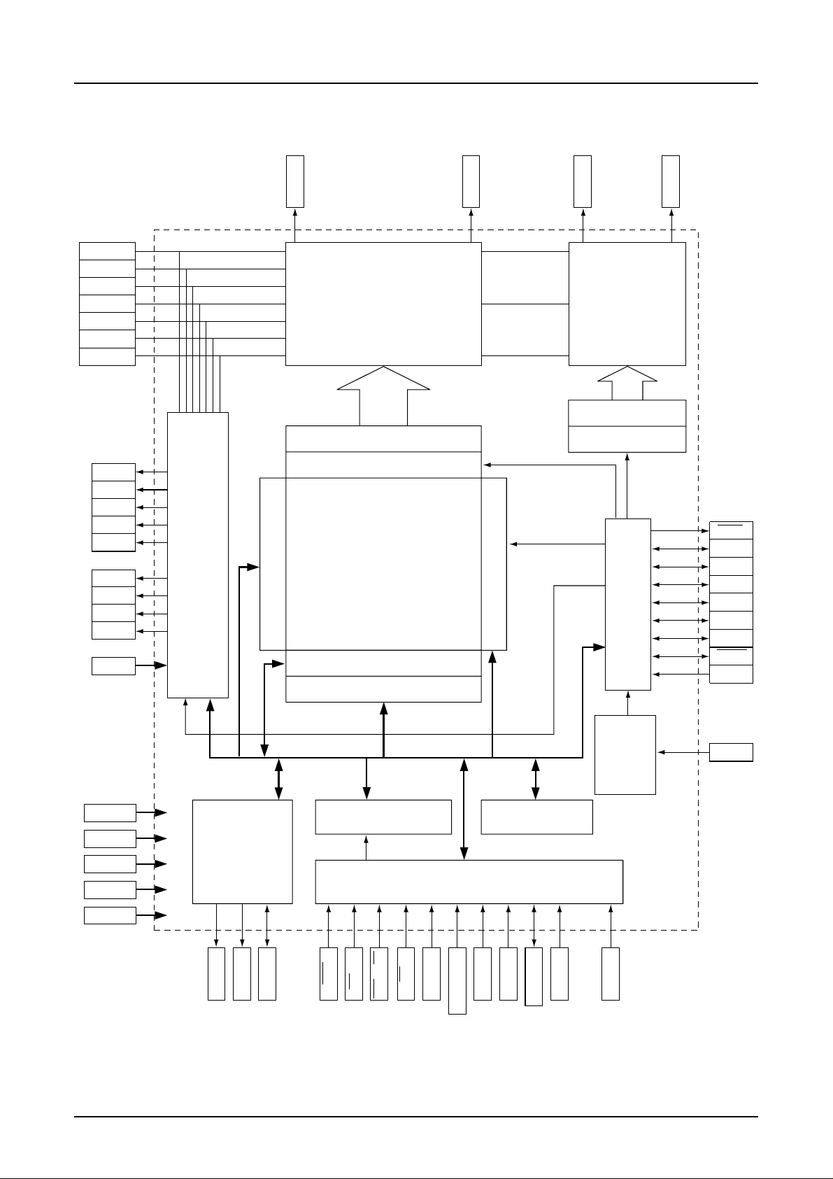
3. BLOCK DIAGRAM
V
3
V
2
V
1
V
C
MV
1
MV2(GND)
MV
3
• • • • • • • • • • • • • • • • • • • • • • • • • • • •
SEG1
SEG396
COM1
SEG Drivers COM Drivers
COM decoder
COM160
CAP1+
CAP1–
CAP2+
CAP2–
V
CAP4+
CAP4–
CAP5+
CPP5–
V
V
DD3
V
V
GND
CLS
DD2
DD
DDI
to
SEG decoder
Shift register
Display data latch
SLP
YSCL
F1,F2
CA
FR
Power circuit
Page address
DDRAM
396 x 168 x 4
Block address
SYNC
CL
DOFF
M/S
I/O buffer
generation circuit
Display timing signal
Column address
Oscillation
circuit
5
Command decoder
Bus holder
CLS
EEPROM
interface
MPU interface
GND2 to
4
RESET
CLOCK
SDA
RES
RD(E)
CS
WR(R/W)
A0
SI
IF1,IF2,IF3
SCL
TEST
D15 to D0
SRCM
2 EPSON Rev. 1.0
4. PIN LAYOUT
b
a
S1D15G00 Series
792
Die No.
1
Y
(0,0)
X
Chip size 25.04 mm × 2.70 mm
Chip thickness 725 µm±25 µm (for reference)
Die No. See Section 5 “List of Device Models.”
Potential on board GND
Bump size Tolerance: bump of the shorter side ±3 µm, bump of the longer side ±4 µm (reference)
Driver output side: 30 µm × 137 µm
Driver input side:
82 µm × 109 µm
Bump pitch Driver output side: 4 2 µm
I/O signal line side:100 µm min.
Bump height 22.5 µm±4 µm (for reference) : S1D15G00D0
B0
*
Alignment coordinate
1 (–11974.2, –639.2)
2 (12091.8, –730.4)
Mark size a = 80 µm
b = 20 µm
205
204
5. LIST OF DEVICE MODELS
Model name Die No. control resistor
S1D15G00D00*100 D15G0D0B Segment: 396 Internal only Unable to read 130 Hz
(#)
S1D15G00D05*100 D15G0D5B controlled via Read enabled
S1D15G00D01*100 D15G0D1B External only × Unable to read
(#)
S1D15G00D06*100 D15G0D6B via VR pin Read enabled
S1D15G00D03*100 D15G0D3B External only × Unable to read 180 Hz
(#)
S1D15G00D08*100 D15G0D8B via VR pin Read enabled
S1D15G00D10*100 D15G0DAB Segment: 300 External only (voltage × Unable to read 130 Hz
(#) Common: 120 via VR pin resistance) /31.2 kHz
Output
count
Common: 160 (voltage electronically /41.6 kHz
V2 voltage
External/Internal
electronic volume)
(voltage controlled
resistance)
(voltage controlled /57.6 kHz
resistance)
Access MPU RAM
to EEPROM
read
(Note)
For “unable to read” models in the above diagram, the MPU cannot read the RAM. If the RAM must be read, use “read
enabled” models.
(#) : These models will be discontinued.
Rev. 1.0 EPSON 3
Frame frequency
/built-in oscillation
frequency
S1D15G00 Series
6. PIN COORDINATE
PAD Pin
No. Name
1NC–12331 –1188.5
2NC–12211
3V
3L –12091
4V3L –11971
5V3L –11851
6V2L –11731
7V2L –11611
8V2L –11491
9V2L –11371
10 V1L –11251
11 V1L –11131
12 V1L –11011
13 V1L –10891
14 VCL –10771
15 VCL –10651
16 VCL –10531
17 VCL –10411
18 VCLSL –10291
19 VCLSL –10171
20 VCLSL –10051
21 VCLSL –9931
22 MV1L –9811
23 MV1L –9691
24 MV1L –9571
25 MV1L –9451
26 MV3L –9331
27 MV3L –9211
28 MV3L –9091
29 TESTA –8971
30 TESTB –8871
31 TESTC –8771
32 TESTD –8671
33 TESTE –8571
34 TESTF –8451
35 TESTF –8336
36 TESTF –8221
37 TESTF –8106
38 TESTF –7991
39 CAP2+ –7871
40 CAP2+ –7756
41 CAP2+ –7641
42 CAP2+ –7526
43 CAP2+ –7411
44 CAP2––7291
45 CAP2––7176
46 CAP2––7061
47 CAP2––6946
48 CAP2––6831
49 CAP1+ –6711
50 CAP1+ –6596
51 CAP1+ –6481
52 CAP1+ –6366
53 CAP1+ –6251
54 CAP1––6131
55 CAP1––6016
56 CAP1––5901
57 CAP1––5786
XY
PAD Pin
No. Name
XY
58 CAP1––5671 –1188.5
59 GND2 –5551
60 GND2 –5446
61 GND2 –5341
62 GND2 –
63 GND2 –
64 GND3 –
5236.05
5131.05
5026.05
65 GND3 –4921
66 GND3 –4816
67 GND –4711
68 GND –4606
69 GND –4501
70 V
DD3 –4396
71 VDD3 –4291
72 VDD4 –4186
73 VDD4 –4081
74 TESTG –3976
75 VDD –3871
76 VDD –3766
77 VDDI –3661
78 VDDI –3556
79 VDDI –3451
80 VDDI –3346
81 FR –3235
82 YSCL –3081
83 F1 –2927
84 F2 –2773
85 DOFF –2619
86 CA –2465
87 SYNC –2311
88 SLP –2157
89 SDA –2003
90 RESET –1849
91 CLOCK –1695
92 TEST1 –1541
93 GND *6 –1387
94 V
DDI *6 –1287
95 CL –1187
96 CLS –1033
97 GND *6 –879
98 VDDI *6 –779
99 CS –679
100 A0 –525
101 GND *6 –371
102 VDDI *6 –271
103 SCL –171
104 SI –17
105 GND *6 137
106 VDDI *6 237
107 D0 337
108 D1 491
109 D2 645
110 D3 799
111 D4 953
112 D5 1107
113 D6 1261
114 D7 1415
Unit: µm
PAD Pin
No. Name
XY
115 GND *6 1569 –1188.5
116 V
DDI *6 1669
117 D8 1769
118 D9 1923
119 D10 2077
120 D11 2231
121 D12 2385
122 D13 2539
123 D14 2693
124 D15 2847
125 GND *6 3001
126 V
DDI *6 3101
127 RD 3201
128 WR 3355
129 GND *6 3509
130 VDDI *6 3609
131 IF1 3709
132 IF2 3863
133 IF3 4017
134 GND *6 4171
135 V
DDI *6 4271
136 RES 4371
137 TESTH 4525
138 MS 4679
139 VDDI 4833
140 VDDI 4938
141 GND 5043
142 GND 5148
143 GND 5253.05
144 GND 5358.05
145 GND4 5463.05
146 GND4 5568.05
147 GND4 5673.05
148 GND4 5778.05
149 GND4 5883.05
150 V
DD 5988.05
151 VDD 6093.05
152 VDD5 6198.05
153 VDD5 6303.05
154 VDD2 6446.05
155 VDD2 6551.05
156 VDD2 6656.05
157 VDD2 6761.05
158 VDD2 6866.05
159 VDD2 6971.05
160 CAP4+ 7113.05
161 CAP4+ 7228.05
162 CAP4+ 7343.05
163 CAP4+ 7458.05
164 CAP4+ 7573.05
165 CAP4– 7693.05
166 CAP4– 7808.05
167 CAP4– 7923.05
168 CAP4– 8038.05
169 CAP4– 8153.05
170 CAP5+ 8273.05
171 CAP5+ 8388.05
4 EPSON Rev. 1.0
S1D15G00 Series
Unit: µm
PAD Pin
No. Name
XY
172 CAP5+ 8503.05 –1188.5
173 CAP5+ 8618.05
174 CAP5+ 8733.05
175 CAP5– 8853
176 CAP5– 8968
177 CAP5– 9083
178 CAP5– 9198
179 CAP5– 9313
180 MV
3R 9433
181 MV3R 9553
Models other than the S1D15G00D10*000 Unit: µm
PAD Pin
No. Name
XY
201 V3R 11953 –1188.5
202 V3R 12073
203 NC 12193
204 NC 12313
205 NC 12327 1177
206 NC 12285
207 COM1 12243
208 COM2 12201
209 COM3 *1
to to
284 COM78 9009
285 COM79 8967
286 COM80 8925
PAD Pin
No. Name
XY
182 MV3R 9673 –1188.5
183 MV1R 9793
184 MV1R 9913
185 MV1R 10033
186 MV1R 10152.9
187
VCLSR/VR*7
10273
188 VCR 10393
189 VCR 10513
190 VCR 10633
191 VCR 10753
PAD Pin
No. Name
XY
287 NC 8883 1177
288 to
299
NC *2
300 NC 8337
301 SEG396 8295
302 SEG395 8253
303 SEG394 *3
to to
694 SEG3 –8211
695 SEG2 –8253
696 SEG1 –8295
697 NC –8337
PAD Pin
No. Name
XY
192 V1R 10873 –1188.5
193 V1R 10993
194 V1R 11113
195 V1R 11233
196 V2R 11353
197 V2R 11473
198 V2R 11593
199 V2R 11713
200 V3R 11833
PAD Pin
No. Name
698 to
709
NC *4
XY
1177
710 NC –8883
711 COM81 –8925
712 COM82 –8967
713 COM83 *5
to to
788 COM158 –12159
789 COM159 –12201
790 COM160 –12243
791 NC –12285
792 NC –12327
S1D15G00D10*000 Unit: µm
PAD Pin
No. Name
XY
201 V3R 11953 –1188.5
202 V3R 12073
203 NC 12193
204 NC 12313
205 NC 12327 1177
206 NC 12285
207 COM1 12243
208 COM2 12201
209 COM3 *1
to to
264 COM58 9849
265 COM59 9807
PAD Pin
No. Name
XY
287 NC 8883 1177
288 to
299
NC *2
300 NC 8337
349 SEG348 6279
350 SEG347 6237
351 SEG346 * 8
to to
649 SEG51
650 SEG50
651 SEG49
697 NC –8337
PAD Pin
No. Name
698 to
709
NC *4
XY
710 NC –8883
711 COM61 –8925
712 COM62 –8967
713 COM63 *5
to to
768
769
770
COM118
COM119
COM120
–11319
–11361
–11403
791 NC –12285
792 NC –12327
1177
266 COM60 9765
*1: You can determine the position on X coordinate from the formula “12159–42* (n–209)”, where the BUMP No. is “n”.
*2: You can determine the position on X coordinate from the formula “8841–42* (n–288)”, where the BUMP No. is “n”.
*3: You can determine the position on X coordinate from the formula “8211–42* (n–303)”, where the BUMP No. is “n”.
*4: You can determine the position on X coordinate from the formula “-8379–42* (n–698)”, where the BUMP No. is “n”.
*5: You can determine the position on X coordinate from the formula “-9009–42* (n–713)”, where the BUMP No. is “n”.
*6: This pin is used to pull up or pull down nearby pins. Thus, it can’t be used for feeding power.
*7: The pin function differs among device models.
External resisting device: It functions as the primary boost voltage output pin (VCLSR).
Internal resisting device: It functions as the regulator inverse input pin (VR).
*8: You can determine the position on X coordinate from formula “6145-42*(n–351)” where the Bump No. is “n”.
Rev. 1.0 EPSON 5

S1D15G00 Series
7. PIN DESCRIPTION
7.1 Power Supply Pins
Pin name I/O Description
Number of
pins
VDDI Input They are used to connect the power for input signals. 6
power
VDD Power They are connected to VCC - the system power. When the system 4
supply power is smaller than 2.6V, they must be connected another 2.6V
or greater power supply.
VDD2 Step-up They are used to connect the power supply for the primary step-up. 6
power The relative magnitude of potential among the pins, namely
VDD2≥VDD≥VDD1, must be observed.
VDD3,VDD5 Power They are power supply pins on the power circuit *1. 4
supply
VDD4 Power They are power supply pins on the oscillation circuit *1. 2
supply
GND Power They are connected to the system ground. 7
supply
GND2, Power They are grounding pins on the power circuit *2. 9
GND4 supply
GND3 Power They are grounding pins on the oscillation circuit *2. 3
supply
V3L, V3R Power These pins are provided on the multi-level power supply for liquid 44
V2L, V2R supply crystal drive. Relative magnitude of potential among the pins,
V1L, V1R namely V3L(R)≥V2L(R)≥V1L(R)≥VCL(R)≥MV1L(R)≥GND≥MV3L(R),
VCL, VCR must be observed.
MV1L, MV
MV3L, MV
1R
3R
When the master operation is turned on or the internal power supply
is turned on, predetermined voltage is output at respective pins.
When S1D15G00 series are used in the master/slave array, they
connect the pins on both the master and slave drivers.
VCLSL Power They are provided on the common driver operating power supply. 4
supply
VCLSR,VR Input Common driver operating power supply/regulator input pins *3. 1
power
*1: Since VDD, VDD3, VDD4 and VDD5 are not internally connected, they must be externally connected to VCC - the
system power.
*2: Since GND, GND2, GND3 and GND4 are not internally connected, they must be externally connected to the system
GND (ground).
*3: The pin function differs among device models.
6 EPSON Rev. 1.0

7.2 Pins on Liquid Crystal Drive Power Circuit
S1D15G00 Series
Pin name I/O Description
CAP1+ O
CAP1– O
CAP2+ O
CAP2– O
CAP4+ O
CAP4– O
CAP5+ O
CAP5– O
They connect the positive going side of the primary step-up capacitor.
They connect the negative going side of the primary step-up capacitor.
They connect the positive going side of the secondary step-up capacitor.
They connect the negative going side of the secondary step-up capacitor.
They connect the positive going side of the tertiary step-up capacitor.
They connect the negative going side of the tertiary step-up capacitor.
They connect the positive going side of the tertiary step-up capacitor.
They connect the positive going side of the tertiary step-up capacitor.
Number of
pins
5
5
5
5
5
5
5
5
Rev. 1.0 EPSON 7
S1D15G00 Series
7.3 MPU Interface Pins
Pin name I/O Description
D15 to D0 I/O They connect to the standard 8-bit or 16-bit MPU bus via the 16
8/16-bit bi-directional bus.
When the following interface is selected and the CS pin is high, the
impedance of the pin becomes high.
1 8-bit parallel: D15-D18 are in the state of high impedance
2 Serial interface: D15-D0 are in the state of high impedance
SI I
SCL I
IF1, IF2 I These pins are used to select either of the MPU interfaces. 3
IF3
A0 I Normally, the least significant bit of the MPU’s address bus is 1
CS I This pin is used to enter chip select signal. It is activated when 1
RD (E) I • It goes active LOW when connected to the 80 series MPU. 1
WR (R/W) I • It goes active LOW when connected to the 80 series MPU. 1
RES I Causing RES to LOW performs initialization. 1
This pin is used to input serial data when the serial interface is selected
This pin is used to input serial clock when the serial interface is selected.
Depending on status of IF1, IF2 and IF3, following selection is made.
IF1 IF2 IF3 MPU interface type
HIGH HIGH HIGH 80 series 16-bit parallel
HIGH HIGH LOW 80 series 8-bit parallel
HIGH LOW LOW 68 series 16-bit parallel
LOW HIGH HIGH 68 series 8-bit parallel
LOW LOW HIGH 9-bit serial
LOW LOW LOW 8-bit serial
connected to identify a parameter or display data from a command.
HIGH: Indicates that data entered to D15 to D0 or SI is a
parameter or display data.
LOW: Indicates that data entered to D15 to D0 or SI is a command.
This function is disabled when the 9-bit serial interface is selected.
CS = LOW, enabling interface with MPU.
This pin is used to connect RD signal from the 80 series MPU. The data
bus is maintained in the output status as long as this signal is LOW.
• It goes active HIGH when connected to the 68 series MPU.
In this case, this pin is used to enter the enable clock from 68 series MPU.
This pin connects WR signal from the 80 series MPU. Signal on
the data bus is latched at the positive going edge of WR signal.
•
This pin enters the read/write signal when connected to the 68 series MPU.
R/W = HIGH: Read
R/W = LOW: Write
Reset operation is performed according the level of RES signal.
Number of
pins
.1
1
8 EPSON Rev. 1.0

7.4 Liquid Crystal Drive Circuit Signals
S1D15G00 Series
Pin name I/O Description
M/S I This pin is used to select either the master or slave operation. 1
M/S = HIGH: Master operation
CLS I It is used to select the display clock. 1
CLS = HIGH: Built-in CR oscillation is used.
CLS = LOW: External clock is used.
When the external clock is used (CLS = LOW), the signal is
entered to CL pin.
CL I/O This pin inputs or outputs the display clock. 1
It outputs the display clock only when M/S = HIGH and CLS = HIGH.
Other than the above: External clock input
FR I/O This pin inputs or outputs the liquid crystal frame signal. 1
M/S = HIGH: Outputs the signal
M/S = LOW: Inputs the signal
SYNC I/O This pin inputs or outputs the liquid crystal synchronization signal. 1
M/S = HIGH: Outputs the signal
M/S = LOW: Inputs the signal
CA I/O This pin inputs or outputs the field start signal. 1
M/S = HIGH: Outputs the signal
M/S = LOW: Inputs the signal
F1, F2 I/O This pin inputs or outputs the drive pattern signal. 1
M/S = HIGH: Outputs the signal
M/S = LOW: Inputs the signal
DOFF I/O This pin is used to control blanking of liquid crystal display. 1
M/S = HIGH: Outputs the signal
M/S = LOW: Inputs the signal
YSCL I/O This pin inputs or outputs the line clock.
M/S = HIGH: Outputs the signal
M/S = LOW: Inputs the signal
SEGn O They output the signal for the segment drive of liquid crystal. 396
COMn O They output the signal for common drive of liquid crystal. 160
Number of
pins
Rev. 1.0 EPSON 9
S1D15G00 Series
7.5 EEPROM Interface Pins
Pin name I/O Description
SDA O Connected to the SDA pin of S1F65170. *11
RESET O Connected to the XRST pin of S1F65170. *11
CLOCK O Connected to the SCK pin of S1F65170. *11
* Always open if the S1F65170 is not used.
Number of
pins
7.6 Control Signals
Pin name I/O Description
SLP O It is the sleep control pin. It outputs LOW level when the sleep-in 1
command is executed.
PO0 O This pin constantly outputs LOW level. It must be maintained open. 1
Number of
pins
7.7 Test Signals
Pin name I/O Description
TESTA to O It is the test pin. 1
TESTG Since it outputs signals, it must be kept open.
TESTH I This pin must be fixed at HIGH or LOW. 1
TEST1 I It is the IC chip test pin. This pin must be fixed at LOW. 1
Number of
pins
10 EPSON Rev. 1.0
S1D15G00 Series
8. FUNCTIONAL DESCRIPTION
8.1 MPU Interfaces
8.1.1 Selecting an MPU Interface Type
S1D15G00 transfers data via the 8/16-bit bi-directional data bus or serial data input.
You can select a desired interface face through the combinations of settings of IF1, IF2 and IF2 as shown in Table 8.1.1.
Table 8.1.1
IF1 IF2 IF3 Interface type CS A0 RD WR D15 to D8 D7 to D0 SI SCL
E R/W
HIGH HIGH HIGH 80 series 16-bit parallel CS A0 RD WR D15 to D8 D7 to D0 ––
HIGH HIGH LOW 80 series 8-bit parallel CS A0 RD WR (HZ) D7 to D0 ––
HIGH LOW LOW 68 series 16-bit parallel CS A0 E R/W D15 to D8 D7 to D0 ––
LOW HIGH HIGH 68 series 8-bit parallel CS A0 E R/W (HZ) D7 to D0 ––
LOW LOW HIGH 9-bit serial CS ––– (HZ) (HZ) SI SCL
LOW LOW LOW 8-bit serial CS A0 –– (HZ) (HZ) SI SCL
– : Must be fixed to either HIGH or LOW.
HZ is in the state of Hight Impedance.
8.1.2 8- or 16-bit Parallel Interface
S1D15G00 identifies type of the data bus signals according to combinations of A0, RD (E) and WR (R/W) signals as
shown in Table 8.1.2.
Table 8.1.2
68 series 80 series
A0 R/W E RD WR Function
1 0 1 1 0 Parameters or display data write.
1 1 1 0 1 Display data read.
0 1 1 0 1 Status read.
0 0 1 1 0 Control data write (command).
Except when the CS=LOW is taking place, D15 to D0 on S1D15G00 are caused to high impedance, disabling input of
A0, RD (E) and WR (R/W).
Relation between Data Bus and Gradation Data
S1D15G00 offers the 256-color display (8 gray-scale) out of 4096 colors as well as the 4096-color display (16 grayscale). When using 256-color display out of 4096 colors, you can specify color for each of R, G and B using the palette
function.
(1) 256-color display out of 4096 colors
Using RGBSET8 command enables you to set color for each of R, G and B by turning on the palette function
prepared to convert 3- or 2-bit data to 4-bit data.
1 8-bit mode
D7, D6, D5, D4, D3, D2, D1, D0: RRRGGGBB (8 bits) data is converted to RRRRGGGGBBBB (12 bits) and then
stored on the display RAM.
2 16-bit mode
D15, D14, D13, D12, D11, D10, D9, D8: RRRGGGBB (8 bits)
D7, D6, D5, D4, D3, D2, D1, D0: RRRGGGBB (8 bits)
Data of two pixels is respectively converted to RRRRGGGGBBBB (12 bits) data and then simultaneously written
to two addresses on the display RAM.
Rev. 1.0 EPSON 11
S1D15G00 Series
4096 color display
1 8-bit mode
D7, D6, D5, D4, D3, D2, D1, D0: RRRRGGGG (8 bits) 1st write
D7, D6, D5, D4, D3, D2, D1, D0: BBBBRRRR (8 bits) 2nd write
D7, D6, D5, D4, D3, D2, D1, D0: GGGGBBBB (8 bits) 3rd write
Data is acquired through write operations as shown above and then that of two pixels is written to the display RAM.
2 16-bit mode
D15, D14, D13, D12, D11, D10, D9, D8, D7, D6, D5, D4, D3, D2, D1, D0: RRRRGGGGBBBBXXXX (12 bits)
Data is acquired through single write operation and then written to the display RAM.
“XXXX” are dummy bits, and they are ignored for display.
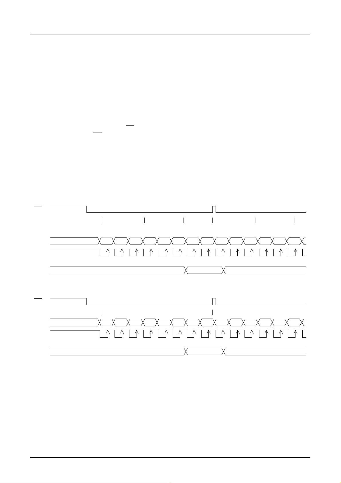
8.1.3 8- and 9-bit Serial Interface
The 8-bit serial interface uses four pins - CS, SI, SCL and A0 - to enter commands and data. Meanwhile, the 9-bit serial
interface uses three pins - CS, SI and SCL - for the same purpose.
Data read is not available with the serial interface. Data entered must be 8 bits. Refer to the following chart for entering
commands, parameters or gray-scale data.
The relation between gray-scale data and data bus in the serial input is the same as that in the 8-bit parallel interface
mode (described in the preceding section) at every gradation.
(1) 8-bit serial interface
When entering data (parameters): A0 = HIGH at the rising edge of the 8th SCL.
CS
dot0(R)
R1R2 R0 G2 G1 G0 B1 B0 R2 R0R1 G2 G1 G0
SI
SCL
12345 678123 4 56
A0
dot1(G)
dot2(B)
When entering command: A0 = LOW at the rising edge of the 8th SCL.
CS
command command
SI
SCL
12345 678123 4 56
A0
dot3(R) dot4(R)
D2D3D4D5D6D7D0D1D2D3D4D5D6D7
D2D3D4D5D6D7D0D1D2D3D4D5D6D7
12 EPSON Rev. 1.0
(2) 9-bit serial interface
When entering data (parameters): SI = HIGH at the rising edge of the 1st SCL.
CS
S1D15G00 Series
SI
SCL
dot0(R)
R2 R1 R0 G2 G1 G0 B1 B0 R2 R1 R0
12345 678912 3 45
dot1(G)
dot2(B)
dot3(R)
D4D5D6D7D/CD0D1D2D3D4D5D6D7D/C
When entering commands: SI = LOW at the rising edge of the 1st SCL.
CS
command command
SI
SCL
12345 678912 3 45
D4D5D6D7D/CD0D1D2D3D4D5D6D7D/C
* If CS is caused to HIGH before 8 bits from D7 to D0 are entered, the data concerned is invalidated. Before entering
succeeding sets of data, you must correctly input the data concerned again.
* In order to avoid data transfer error due to incoming noise, it is recommended to set CS at HIGH on byte basis to
initialize the serial-to-parallel conversion counter and the register.
Rev. 1.0 EPSON 13
S1D15G00 Series
8.2 Access to DDRAM and Internal Registers
S1G15G00 realizes high-speed data transfer because the access from MPU is a sort of pipeline processing done via the
bus holder attached to the internal, requiring the cycle time alone without needing the wait time.
For example, when MPU writes data to the DDRAM, the data is once held by the bus holder and then written to the
DDRAM before the succeeding write cycle is started. When MPU reads data from the DDRAM, the first read cycle
is dummy and the data read in the dummy cycle is held by the bus holder, and then it is read from the bus holder to the
system bus in the succeeding read cycle. Fig. 8.2.1 illustrates these relations.
* Write operation
A0
tcyc
WR
MPU
DATA
Bus holder
Internal
Data write
signal
* Read operation
A0
WR
RD
MPU
Command write Data write Data write
Command write
Dummy read Data read
External pulse
Bus holder
Internal
Data Read
signal
Command
RAM dataRAM data
Fig. 8.2.1
* There is a restriction in the read sequence of the DDRAM. Namely, the data at the specified address is not output
in the first data read conducted immediately after the memory read command (dummy read). It is read in the second
data read.
14 EPSON Rev. 1.0
S1D15G00 Series
8.3 DDRAM
8.3.1 DDRAM
It is 396 × 168 × 4 bits capacity RAM prepared for storing dot data. You can access a desired bit by specifying the page
address and column address.
Since display data from MPU - D7 to D0 and D1 to D8 - correspond to one or two pixels of RGB, data transfer-related
restrictions are reduced, realizing the display flexibly.
The RAM on S1D15G00 is separated to a block per 4 line to allow the display system to process data on the block basis.
MPU’s read and write operations to and from the RAM are performed via the I/O buffer circuit. Reading of the RAM
for the liquid crystal drive is controlled from another separate circuit.
Refer to the following memory map for the RAM configuration.
1Models other than the S1D15G00D10*100 (models that have 132 RGB × 160 output)
Memory Map (When using the 8 gray-scale. 8-bit mode)
RGB alignment (Command of data control parameter2=000)
Column
LCD
read
direction
Block
0 0 167
P11:0
P11:1
Color
Page
P10:0 P10:1
Data
D7
D6
D5
0
131
GB
D4
D1D0D7
D3
D2
D6
D5
1
132
D4
D3
D2
D1
D0
RGBRGBR
D7
D6
D5
131
0
D4
D3
D2
D1
D0
1
2
40
41
1 166
2 165
3 164
4 163
5 162
6 161
7 160
8 159
9 158
160 7
161 6
162 5
163 4
164 3
165 2
166 1
167 0
SEGout
123456 394395396
Each of RGB data entered to D7 to D0 (3 or 2 bits) is converted to 4 bits before written to the RAM. You can change
position of R and B with DATCTL command.
Rev. 1.0 EPSON 15
S1D15G00 Series
Memory Map (When using the 8 gray-scale, 16-bit mode)
RGB alignment (Command of data control parameter2=000)
Column
LCD
read
direction
Block
0
1
2
P11: 0
P11: 1
Color
Data
Page
P10:0 P10:1
0 167
1 166
2 165
3 164
4 163
5 162
6 161
7 160
8 159
R
D15
D14
D13
0
65
G
BRGBRGBRGB RGB
D12
D9
D11
D8
D10
011
65 64 64 0
D15
D12
D7
D6
D5
D4
D3
D2
D1
D0
D14
D13
D9D8D7
D11
D10
D6
D5
D4
D3
D2
D1
D0
D7
D6
D5
65
D4
D3
D2
D1
D0
9 158
40
41
SEGout
160 7
161 6
162 5
163 4
164 3
165 2
166 1
167 0
123456789101112 394395396
Each of RGB data entered to D7 to D0 (3 or 2 bits) is converted to 4 bits before written to the RAM. You can change
position of R and B with DATCTL command.
16 EPSON Rev. 1.0
Memory Map (When using the 16 gray-scale 8-bit mode)
RGB alignment (Command of data control parameter2=000)
S1D15G00 Series
Column
LCD
read
direction
Block
0
1
2
P11: 0
P11: 1
Color
Data
Page
P10:0 P10:1
0 167
1 166
2 165
3 164
4 163
5 162
6 161
7 160
8 159
0
65
R1 G1 B1 R2 G2 B2 R1 G1 B1 R G2 B2 R2 G2 B2
D7
D3
D7
D6
D2
D6
D5
D1
D5
D4
D0
D4
011
65 64 64 0
D3
D2
D1
D0
D7
D6
D5
D4
D3
D2
D1
D0
D7
D6
D5
D4
D3
D2
D1
D0
D7
D6
D5
D4
D3
D2
D1
D0
D7
D6
D5
D4
D3
D2
D1
D0
D3
D2
D1
D0
65
D7
D6
D5
D4
D3
D2
D1
D0
9 158
40
41
SEGout
160 7
161 6
162 5
163 4
164 3
165 2
166 1
167 0
1 2 3 4 5 6 7 8 9 10 11 12 394 395 396
You can change position of R and B with DATCTL command.
Rev. 1.0 EPSON 17

S1D15G00 Series
Memory Map (When using the 16 gray-scale 16-bit mode)
RGB alignment (Command of data control parameter2=000)
LCD
read
direction
Block
0 0 167
P11:0
P11:1
Color
Data
Page
P10:0 P10:1
1 166
2 165
3 164
D15
D14
D13
D12
0
131
GB
D11
D7
D10
D6
D9
D5
D8
D4
D15
D14
D13
D12
1
130
D11
D10
D9
D8
D7
D6
D5
D4
Column
RGBRG BR
D15
D14
D13
D12
131
D11
D10
D9
D8
0
D7
D6
D5
D4
1
2
40
41
4 163
5 162
6 161
7 160
8 159
9 158
160 7
161 6
162 5
163 4
164 3
165 2
166 1
167 0
SEGout
123456 394395396
You can change position of R and B with DATCTL command
18 EPSON Rev. 1.0

2 S1D15G00D10*100 (100 RGB × 120 output)
Memory map (when 8-tone, 8-bit mode is used)
RGB alignment (Command of data control parameter2=000)
LCD
read
direction
Block
0 0 167
P11:0
P11:1
Color
Page
P10:0 P10:1
1 166
2 165
3 164
Data
D7
D6
D5
16
115
GB
D4
D1D0D7
D3
D2
D6
D5
17
114
D4
D3
D2
D1
D0
Column
S1D15G00 Series
115
16
RGBRGBR
D7
D4
D1
D6
D3
D0
D5
D2
1
2
28
29
SEGout
4 163
5 162
6 161
7 160
8 159
9 158
112 55
113 54
114 53
115 52
116 51
117 50
118 49
119 48
49 50 51 52 53 54 346 347 348
Although data is described as D7 - D0 (3 bits or 2 bits), all RGB data will be converted to 4 bits and written to the RAM.
Positions of R and B can be changed using the DATCTL command.
Rev. 1.0 EPSON 19

S1D15G00 Series
Memory map (when 8-tone, 16-bit mode is used)
RGB alignment (Command of data control parameter2=000)
Column
LCD
read
direction
Block
0
1
2
P11: 0
P11: 1
Color
Page
P10:0 P10:1
0 167
1 166
2 165
3 164
4 163
5 162
6 161
7 160
8 159
9 158
Data
R
D15
D14
D13
8
57
BRGBRGBRGB RGB
G
D9
D12
D8
D11
D10
899
57 56 56 8
D1
D7
D6
D5
D4
D3
D2
D0
D15
D14
D13
D12
D11
D10
D9D8D7
D6
D5
D4
D3
D2
D1
D0
D7
D6
D5
57
D4
D3
D2
D1
D0
28
29
SEGout
112 55
113 54
114 53
115 52
116 51
117 50
118 49
119 48
49 50 51 52 53 54 55 56 57 58 59 60 346 347 348
Although data is described as D7 - D0 (3 bits or 2 bits), all RGB data will be converted to 4 bits and written to the RAM.
Positions of R and B can be changed using the DATCTL command.
20 EPSON Rev. 1.0

Memory map (when 16-tone, 8-bit mode is used)
RGB alignment (Command of data control parameter2=000)
S1D15G00 Series
Column
LCD
read
direction
Block
0
1
2
P11: 0
P11: 1
Color
Data
Page
P10:0 P10:1
0 167
1 166
2 165
3 164
4 163
5 162
6 161
7 160
8 159
8
57
R1 G1 B1 R2 G2 B2 R1 G1 B1 R2 G2 B2 R2 G2 B2
D7
D3
D7
D6
D2
D6
D5
D1
D5
D4
D0
D4
899
57 56 56 8
D3
D2
D1
D0
D7
D6
D5
D4
D3
D2
D1
D0
D7
D6
D5
D4
D3
D2
D1
D0
D7
D6
D5
D4
D3
D2
D1
D0
D7
D6
D5
D4
D3
D2
D1
D0
D3
D2
D1
D0
57
D7
D6
D5
D4
D3
D2
D1
D0
9 158
28
29
SEGout
112 55
113 54
114 53
115 52
116 51
117 50
118 49
119 48
49 50 51 52 53 54 55 56 57 58 59 60 346 347 348
Positions of R and B can be changed using the DATCTL command.
Rev. 1.0 EPSON 21

S1D15G00 Series
Memory map (when 16-tone, 16-bit mode is used)
RGB alignment (Command of data control parameter2=000)
LCD
read
direction
Block
0 0 167
P11:0
P11:1
Color
Page
P10:0 P10:1
Data
1 166
2 165
3 164
D15
D14
D13
D12
16
115
GB
D7
D11
D6
D10
D5
D9
D4
D8
D15
D14
D13
D12
17
114
D11
D10
D9
D8
D7
D6
D5
D4
Column
D1
D1
D1
D1
115
16
RGBRG BR
D7
D11
D6
D10
D5
D9
D4
D8
1
2
28
29
4 163
5 162
6 161
7 160
8 159
9 158
112 55
113 54
114 53
115 52
116 51
117 50
118 49
119 48
SEGout
49 50 51 52 53 54 346 347 348
Positions of R and B can be changed using the DATCTL command.
22 EPSON Rev. 1.0

S1D15G00 Series
8.3.2 Page Address Control Circuit
This circuit is used to control the address in the page direction when MPU accesses the DDRAM or when reading the
DDRAM to display image on the LCD.
You can specify a scope of the page address (start and end page) with PASET (page address set) command. When the
page-direction scan is specified with DATCTL (data control) command and the addresses are incremented from the start
up to the end page, the column address is incremented by 1 and the page address returns to the start page.
The DDRAM supports up to 168 lines
*1: S1D15G00D10*000 supports up to 120 lines and the total number of pages is 120.
In the read operation, as the end page is reached, the column address is automatically incremented by 1 and the page
address is returned to the start page.
Using the address normal/inverse parameter of DATCTL command allows you to inverse the correspondence between
the DDRAM address and common output.
8.3.3 Column Address Control Circuit
This circuit is used to control the address in the column direction when MPU accesses the DDRAM. You can specify
a scope of the column address (start and end column) using CASET (column address set). When the column-direction
scan is specified with DATCTL command and the addresses are incremented from the start to the end up to the end
column, the page address is incremented by 1 and the column address returns to the start column.
In the read operation, too, the column address is automatically incremented by 1 and returns to the start page as the end
column is reached.
Just like the page address control circuit, using the column address normal/inverse parameter of DATCTL command
enables to inverse the correspondence between the DDRAM column address and segment output. This arrangement
relaxes restrictions in the chip layout on the LCD module.
*1
, and thus the total page becomes 168.
8.3.4 I/O Buffer Circuit
It is the bi-directional buffer used when MPU reads or writes the DDRAM. Since MPU’s read or write of the DDRAM
is performed independently from data output to the display data latch circuit, asynchronous access to the DDRAM while
the LCD is turned on does not cause troubles such as flicking of the display images.
8.3.5 Block Address Circuit
This circuit associates pages on the DDRAM with COM output. S1D15G00 processes signals for the liquid crystal
display on 4-page basis (block basis). Thus, when specifying a specific area in the area scroll display or partial display,
you must designate it in block.
8.3.6 Display Data Latch Circuit
This circuit is used to temporarily hold display data to be output from the DDRAM to the SEG decoder circuit. Since
DISNOR/DISINV (display normal/inverse) and DISON/DISOFF (display on/display off) commands are used to
control data in the latch circuit alone, they do not modify data in the DDRAM.
Rev. 1.0 EPSON 23

S1D15G00 Series
8.4 Area Scroll Display
Using ASCSET (area scroll set) and SCSTART (scroll start set) commands allows you to scroll the display screen
partially. You can select any one of the following four scroll patterns.
Center screen scroll Top screen scroll Bottom screen scroll Whole screen scroll
: Fixed area
: Scroll area
Fig. 8.4.1
When, for example, 1/128 duty (Display area: 32 blocks = 128 lines) is selected, and the top 2 blocks = 8 lines and bottom
2 blocks = 8 lines are specified as the fixed areas and the remaining 28 blocks = 112 lines as the scroll area, 10 blocks
= 40 lines on the DDRAM can be used as the background area.
DDRAM block
0
1
2
LCD panel
32 blocks
=128 line
29
30
39
40
41
Fixed area
Display area
Scroll area
Background area
24 EPSON Rev. 1.0

S1D15G00 Series
8.5 Partial Display
Using PTLIN (partial in) command allows you to turn on the partial display (division by line) of the screen. This mode
requires less current consumption than the whole screen display, making it suitable for the mobile equipment in the
standby state.
: Display area (partial display area)
: Non-display area
8.6 Gray-Scale Display
This function represents gray-scale by frame modulating the gray-scale date written on the display data RAM. In the
256-out-of-4096 colors (8 gray-scale) display, you can specify display colors using the command.
Normally black liquid crystal in the reverse display mode - 8 gray scale display
R (D7,D6,D5)
G (D4,D3,D2)
B (D1,D0)
Black
(0,0,0) (0,0,1) (0,1,0) (0,1,1) (1,0,0) (1,0,1) (1,1,0) (1,1,1)
Black
(0,0,0) (0,0,1) (0,1,0) (0,1,1) (1,0,0) (1,0,1) (1,1,0) (1,1,1)
Black
(0,0) (0,1) (0,1) (0,1) (1,0) (1,0) (1,0) (1,1)
Any one of above
Any one of above
Red
Green
Blue
Respective data on red, green and blue are converted to the display data to be specified by the parameters of RGBSET8
command, and then written to the DDRAM. Blue is displayed in 4 gray-scale.
8.7 Oscillation Circuit
S1G15G00 contains the oscillation circuit whose operation does not require any external part. The oscillation circuit
is enabled only when M/S = HIGH and CLS = HIGH. When the external clock signal is (CLS = LOW or M/S = LOW),
the clock is entered from CL pin.
8.8 Display Timing Generation Circuit
This circuit generates the timing signal for display (CL, FR, SYNC, CA, F1, F2, DOFF) using the clock from the builtin oscillation circuit or the external clock.
It is also used to generate the clock to turn on the liquid crystal-drive power circuit.
When using S1D15G00 in multi-chip array, the display timing signal (CL, FR, SYNC, CA, F1, F2, DOFF) must be sent
from the master to the slave.
8.9 SEG Decoder Circuit
This circuit outputs the segment driver control signal based on display data for 4-page and the timing signal.
8.10 Liquid Crystal Drive Circuit
It outputs liquid crystal drive voltage. Responding to the decoder output signal and the display-timing signal, the
segment output pin outputs one of potentials V2, V1, VC, MV1 or MV2 and the common output pin outputs one of
potentials V3, VC or MV3.
Rev. 1.0 EPSON 25

S1D15G00 Series
8.11 Liquid Crystal-Drive Power Circuit
The power circuit contained in S1D15G00 generates voltage required to drive liquid crystal. This low power
consumption type power circuit is consisted the voltage regulator, booster circuits (primary, secondary) and voltage
follower. The power circuit is enabled only when the master operation mode is turned on.
The power control circuit turns on or off the voltage regulator, booster circuits, Reference voltage generation circuit
and voltage follower responding to PWRCTR (power control set) command. Thus, function of the external and internal
power supplies can be partly used in parallel.
Table 8.11.1 lists the functions controlled by the 4-bit data - parameter of PWRCTR. Table 8.11.2 shows combinations
of 4 bits (combinations shown in Table 8.11.2 alone are valid).
Table 8.11.1
Item State
“1” “0”
D3 Primary booster circuits control bit ON OFF
D2 Secondary booster circuit control bit ON OFF
D1 Reference voltage generation circuit control bit ON OFF
D0 Voltage adjusting circuit/Voltage follower control bit ON OFF
Table 8.11.2
Function turned on D3 D2 D1 D0
External power input pins
1. Entire built-in power circuit is turned on 1 1 1 1 –
2. Other than the secondary booster and step-down circuits 1 0 1 1 V3, MV3
3. External power supply alone 0 0 0 0 V3, V2, VC, MV1, MV3
8.11.2 Voltage Transform Circuit
The charge pump booster circuit and the operational amplifier’s voltage follower generate each potential required to
drive the liquid crystal based on the reference voltage generated by the voltage regulator.
Ground potentials (abbreviated as GND in the following description) of the power circuit in the IC are GND2 and
GND4.
Fig. 8.11.1 illustrates mutual relationship between potentials.
Secondary
Primary
boorster circuit
V
DD2
VCLS
V2 V1, VC, MV1,
generation circuit
boorster circuit
V
V2
V1
VC
3
MV1
GND
Secondary
boorster circuit
MV2
MV3
Fig. 8.11.1 Mutual Relationship between Voltage Transform Circuits
26 EPSON Rev. 1.0

S1D15G00 Series
Table 8.11.3 shows the theoretical expression of respective potentials. Since these are theoretical values, they can differ
from actual voltages depending on load on the liquid crystal.
Table 8.11.3 Theoretical Expression of Potentials
Signal name Theoretical expression Theoretical expression
(relative to GND = 0V) (relative to VC = 0V)
V3 2×(V2–GND) 2×(VC–GND)
V2 Output from voltage regulator VC–GND
V1 3/4×(V2–GND) 1/2×(VC–GND)
VC 2/3×(V2–GND) 0V
MV1 1/3×(V2–GND) –1/2×(VC–GND)
GND(MV2)0V –(VC–GND)
MV3 –(V2–GND) –2×(VC–GND)
8.11.3 Primary Booster Circuit
The built-in booster circuit triples the voltage of VDD2-GND.
VDD2-GND voltage is tripled by capacitor C connected across CAP1+ and CAP1,CAP2+ and CAP2- as well as VCSL
and GND (or VDD2), and then output at VCSL pin.
In the case of double boosting, short circuit the CAP2+ and VCSL pin.
Fig. 8.11.2 shows how the voltage is stepped up by the capacitors connected.
CSL=
3xV
C
+
C
+
C
+
GND or V
V
CAP2—
CAP2+
CAP1—
CAP1+
CSL
DD2
V
DD2
GND
V
DD2
C
+
C
+
GND or V
V
CAP2—
CAP2+
CAP1—
CAP1+
CLS
DD2
V
DD2
GND
V
CLS=
2xV
DD2
Fig. 8.11.2 Relation between Capacitors and Voltage Step-up
8.11.4 Voltage Regulator Circuit
The voltage regulator circuit generates the liquid crystal drive voltage V2 using VCSL from the primary booster circuit.
S1D15G00 incorporates the high-precision constant voltage source, 64-step electronic volume control function and
resistor to regulate V2 voltage. The voltage regulator circuit covers a wider temperature range with fewer numbers of
parts thanks to the temperature gradient control function as well as the temperature sensing function.
However, capacitors may be required for voltage regulation between V2 and GND pins due to the load of LCD panel.
Insert the capacitors, if necessary, by observing the voltage waveforms and current consumption.
1 Built-in Resistor for V2 Voltage Regulation
The contents described in this document apply only to models that use a V2 voltage control resistor inside the IC.
Using this resistor and the electronic volume control function allows you to control the liquid crystal drive voltage V2
to an optimum level for the LCD panel with the command alone, without resorting to external resistors.
V2 output voltage can be determined from Equation A-1 as long as the relation V2 < VCSL is met.
However, set the voltage of V2 by allowing for a drop in the voltage due to load, so that it becomes at or below 80 %
of VCSL.
Rb
V
111
=+
V
EV REG2
•=+
Ra
Rb
Ra
•
α
218
2
+
•–
(Equation A-1)
V
Note: VREG is the constant voltage source inside the IC. It is 1.2V (Typ.) at Ta = 25°C.
Rev. 1.0 EPSON 27

S1D15G00 Series
VCSL
VEV (Constant voltage source +
Electronic volume controller)
Built-in Rb
Built-in Ra
GND
V2
Fig. 8.11.3 Voltage Regulator Circuit
Rb/Ra in Equation A-1 is the resistance ratio of the built-in V2 voltage-regulating resistance. This ratio can be varied
in 8 levels by changing parameters 2(P2) of electronic volum control command. Reference ratios of “1 + Rb/Ra” are
shown in Table 8.11.4.
Table 8.11.4 Resistance Ratio of Built-in V2 Voltage-Regulating Resistance: Parameters and “1+
R/Ra” Ratio (For reference)
Parameter
P22 P21 P20
1+Rb/Ra ratio V1 voltage value
0 0 0 3.95 Small
0 0 1 4.27
0 1 0 4.60 •
0 1 1 4.93 •
1 0 0 5.26 •
1 0 1 5.59 •
1 1 0 5.92
1 1 1 6.25 Large
2V2 voltage control external resistor
The contents described in this document apply only to models that use an external V2 voltage control resistor.
If you use an external resistance control model, you can set the V2 voltage using an external resistor.
Use a semi-fixed resistor for V2 voltage regulation.
CSL
V
VEV
(Fixed voltage source and
Electronic volume control)
GND
+
–
VR
V
2
GND
V
2
External resistor Rb
External resistor Ra
Fig. 8.11.4 Voltage Regulator Circuit
Select the external Ra and Rb values to allow stable voltage supply by observing the V2 voltage waveforms.
As the VR pin has a high input impedance and it is susceptible to ambient noise, the resistors and their leads must be
placed in a short distance and they must be away from the clock source.
3Constant Voltage Source and Electronic Volume Control Circuit
The constant voltage source generates V
REG - the reference voltage inside the IC. You can specify one of four types
of temperature gradients with parameters of electronic volum control command. See Fig. 8.11.5.
28 EPSON Rev. 1.0

Table 8.11.5 Parameters and VREG Temperature Gradient
S1D15G00 Series
Parameter
Temperature gradient (%/C)
00 –0.05
01 –0.1
10 –0.15
11 –0.2
The electronic volume control circuit varies α in Equation A-1 according to parameters 1(P1) of electronic volum
control command. Table 8.11.6 lists relation between the parameters and α.
Table 8.11.6 Parameters and Electronic Volume
Parameter
P15 P14 P13 P12 P11 P10
α
V1 voltage value
000000 63 Small
000001 62
000010 61
•••
•••
•••
111101 2
111110 1
111111 0
Large
8.11.5 Voltage Divider/Voltage Follower Circuit
The voltage divider/voltage follower circuit V2 output from the voltage regulator circuit and then generates liquid
crystal drive voltages V1,VC and MV1 using the operational amplifier-featured voltage follower.
Capacitors may be required for voltage regulation between the GND and each of V1, VC and MV1 pins due to the load
of LCD panel. Insert the capacitors, if necessary, by observing the voltage waveforms and current consumption.
V1 = 3/4×V2
VC = 2/4×V2
MV1 = 1/4×V2
8.11.6 Secondary Booster Circuit and Tertiary Booster/Step-Down Circuit
The secondary booster circuit boosts or steps down based on V2 and produces V3 and MV3.
Their potential relationship is expressed with the following theoretical equation:
V3 = 2×V2
MV3 = –V2
8.11.7 Samples of Connections Peripheral to Power Circuit (For your information)
Following illustrates the connections when the entire power circuit is used.
Sample of common setting
Item Setting Unit
C1 1.0 to 4.7 µF
C2 0.47 to 1.0
Optimum values of C1 and C2 above vary
depending on the LCD panel to be driven.
Above values should be referenced as
information only. It is recommended to
check how patterns with high load are
displayed before finalizing the values.
C between V
DD2 and GND signifies a
C1
C1
C1
C1
+
+
+
+
CAP1+
CAP1–
CAP2+
CAP2–
CAP4+
CAP4–
CAP5+
CAP5–
VDD2
VCSL
GND
V
V2
V1
VC
MV1
MV3
+
+
3
+
C1
C2
2
2
bias capacitor.
Rev. 1.0 EPSON 29

S1D15G00 Series
9. COMMANDS
9.1 Command List
Following table lists the control signals and commands using the 80 series interface as the example.
Command A0 RD WR D7 D6 D5 D4 D3 D2 D1 D0 Function Hex
1 DISON 01010101111Display on AF None
2 DISOFF 01010101110Display off AE None
3 DISNOR 01010100110Normal display A6 None
4DISINV 01010100111Inverse display A7 None
5COMSCN01010111011Common scan direction BB 1byte
6 DISCTL 01011001010Display control CA 3byte
7 SLPIN 01010010101Sleep in 95 None
8 SLPOUT 01010010100Sleep out 94 None
9 PASET 01001110101Page address set 75 2byte
10 CASET 01000010101Column address set 15 2byte
11 DATCTL 01010111100Data scan direction, etc. BC 3byte
12
RGBSET8
13 RAMWR 01001011100Writing to memory 5C Data
14 RAMRD 01001011101Reading from memory 5D Data
15 PTLIN 01010101000Partial display in A8 2byte
16 PTLOUT 01010101001Partial display out A9 None
01011001110256-color position set CE 20byte
Parameter
17RMWIN 01011100000Read and modify write E0 None
18 RMWOUT 01011101110End EE None
19 ASCSET 01010101010Area scroll set AA 4byte
20 SCSTART 01010101011Scroll start set AB 1byte
21 OSCON 01011010001Internal oscillation on D1 None
22 OSCOFF 01011010010Internal oscillation off D2 None
23 PWRCTR 01000100000Power control 20 1byte
24 VOLCTR 01010000001Electronic volume control 81 2byte
25 VOLUP 01011010110
26
VOLDOWN
27TMPGRD01010000010Temperature gradient set 82 1 byte
28EPCTIN 01011001101Control EEPROM CD 1 byte
29EPCOUT01011001100Cancel EEPROM control CC None
30 EPMWR 01011111100Write into EEPROM FC None
31 EPMRD 01011111101Read from EEPROM FD None
32
EPSRRD1
33
EPSRRD2
34NOP 01000100101NOP instruction 25 None
01011010111
01001111100Read register 1 7C None
01001111101Read register 2 7D None
Increment electronic control by 1
Decrement electronic control by 1
D6 None
D7 None
35 STREAD 0 0 1 Status Status read
30 EPSON Rev. 1.0

S1D15G00 Series
(1) Display ON (DISON) Command: 1 Parameter: None
It is used to turn the display on. When the display is turned on, segment outputs and common outputs are generated
at the level corresponding to the display data and display timing. You can’t turn on the display as long as the sleep mode
is selected. Thus, whenever using this command, you must cancel the sleep mode first.
A0 RD WR D7 D6 D5 D4 D3 D2 D1 D0
Command 01010101111
(2) Display OFF (DISOFF) Command: 1 Parameter: 0
It is used to forcibly turn the display off. As long as the display is turned off, every segment and common outputs are
forced to VC level and DOFF pin is caused to LOW.
A0 RD WR D7 D6 D5 D4 D3 D2 D1 D0
Command 01010101110
(3) Normal display (DISNOR) Command: 1 Parameter: 0
It is used to normally highlight the display area without modifying contents of the display data RAM.
A0 RD WR D7 D6 D5 D4 D3 D2 D1 D0
Command 01010100110
(4) Inverse display (DISINV) Command: 1 Parameter: 0
It is used to inversely highlight the display area without modifying contents of the display data RAM. This command
does not invert non-display areas in case of using partial display.
A0 RD WR D7 D6 D5 D4 D3 D2 D1 D0
Command 01010100111
(5) Common scan (COMSCAN) Command: 1 Parameter: 1
It is used to specify the common output scan direction. This command helps increasing degrees of freedom of wiring
on the LCD panel.
A0 RD WR D7 D6 D5 D4 D3 D2 D1 D0 Function
Command 01010111011
Parameter1 (P1)
When 1/160 is selected for the display duty, pins and common output are scanned in the order shown below.
P12 P11 P10 Common scan direction
000 1 → 80 81 → 160
001 1 → 80 160 ← 81
010 80 ← 181→ 160
011 80 ← 1 160 ← 81
110*****P12 P11 P10 Common scan direction
COM1 pin COM80 pin COM81 pin COM160 pin
Rev. 1.0 EPSON 31

S1D15G00 Series
(6) Display control (DISCTL) Command: 1 Parameter: 3
This command and succeeding parameters are used to perform the display timing-related setups. This command must
be selected before using SLPOUT. Don’t change this command while the display is turned on.
A0 RD WR D7 D6 D5 D4 D3 D2 D1 D0 Function
Command 01011001010
Parameter1 (P1)
Parameter2 (P2)
Parameter3 (P3)
P1: It is used to specify the CL dividing ratio, F1 and F2 drive-pattern switching period.
P13, P12: CL dividing ratio. They are used to change number of dividing stages of external or internal clock.
P13 P12 CL dividing ratio
0 0 2 divisions (default)
0 1 4 divisions
1 0 8 divisions
1 1 Not divide
110****P13 P12 P11 P10 CL dividing ratio, F1 and
F2 drive pattern.
110**P25 P24 P23 P22 P21 P20 Drive duty
110***1 P33 P32 P31 P30 FR inverse-set value
*: Invalid bits irrelevant to the operation.
P11, P10: They are used to change F1 and F2 drive-pattern switching period.
P11 P10 F1, F2 switching period
0 0 8H (default)
01 4H
1 0 16H
1 1 Field
P2: It is used to specify the duty of the module on block basis.
Duty **P25 P24 P23 P22 P21 P20 (Numbers of display lines)/4-1
Example: 1/128 duty 00011111 128/4–1=31
Example: 1/160 duty 00100111 160/4–1=39
P3: It is used to specify number of lines to be inversely highlighted on LCD panel (lines can be inversely highlighted
in the range of 2 to 16)
Inversely highlighted lines
Example: 11H 00001010 11–1=10
Example: 13H 00001100 13–1=12
In the default, 11H inverse highlight is selected.
(7) Seep in (SLPIN) Command: 1 Parameter: 0
Entering this command generates LOW at SLP pin.
**P25 P24 P23 P22 P21 P20 Inversely highlighted lines –1
A0 RD WR D7 D6 D5 D4 D3 D2 D1 D0
Command 01010010101
DOFF (LCD panel blanking control pin) on S1D15G00 is caused to LOW when the sleep in mode is turned on.
The LCD power supply and the boost circuit output is jumpered with GND during Sleep In.
32 EPSON Rev. 1.0

S1D15G00 Series
(8) Sleep out (SLPOUT) Command: 1 Parameter: 0
Entering this command generates HIGH at SLP pin.
A0 RD WR D7 D6 D5 D4 D3 D2 D1 D0
Command 01010010100
(9) Page address set (PASET) Command: 1 Parameter: 2
When MPU makes access to the display data RAM, this command and succeeding parameters are used to specify the
page address area. As the addresses are incremented from the start to the end page in the page-direction scan, the column
address is incremented by 1 and the page address is returned to the start page. Note that the start and end page must
be specified as a pair. Also, the relation “start page < end page” must be maintained.
A0 RD WR D7 D6 D5 D4 D3 D2 D1 D0 Function
Command 01001110101
Parameter1 (P1)
Parameter2 (P2)
(10) Column address set (CASET) Command: 1 Parameter: 2
When MPU makes access to the display data RAM, this command and succeeding parameters are used to specify the
column address area. As the addresses are incremented from the start to the end column in the column-direction scan,
the page address is incremented by 1 and the column address is returned to the start column. Note that the start and end
page must be specified as a pair. Also, the relation “start column < end column” must be maintained.
1 1 0 P17 P16 P15 P14 P13 P12 P11 P10 Start page
1 1 0 P27 P26 P25 P24 P23 P22 P21 P20 End page
A0 RD WR D7 D6 D5 D4 D3 D2 D1 D0 Function
Command 01000010101
Parameter1 (P1)
Parameter2 (P2)
* Note that in the 8- and16-bit access, or 8 and 16 gray-scale, a different approach is employed for specifying the address.
1 1 0 P17 P16 P15 P14 P13 P12 P11 P10 Start address
1 1 0 P27 P26 P25 P24 P23 P22 P21 P20 End address
Rev. 1.0 EPSON 33

S1D15G00 Series
(11) Data control (DATCTL) Command: 1 Parameters: 2
This command and succeeding parameters are used to perform various setups needed when MPU operates display data
stored on the built-in RAM.
A0 RD WR D7 D6 D5 D4 D3 D2 D1 D0 Function
Command 01010111100
Parameter1 (P1)
Parameter2 (P2)
Parameter3 (P3)
P1: It is used to specify the normal or inverse display of the page address and also to specify the page address scanning
direction.
P10: Normal/inverse display of the page address. P10 = 0: Normal and P10 = “1”: Inverse.
P11: Normal/reverse turn of column address. P11 = “0”: Normal rotation and P11 = “1”: Reverse rotation
P12: Address-scan direction. P12 = “0”: In the column direction and P12 = “1”: In the page direction.
P2: RGB arrangement. This parameter allows you to change RGB arrangement of the segment output according to RGB
arrangement on the LCD panel. In this case, writing position of data {R = (D7, D6, D5), G = (D4, D3, D2), B =
(D1, D0)} on the display memory is changed.
110*****P12 P11 P10
Normal/inverse display of page
address and page-address
scan direction.
110*****P22 P21 P20 RGB arrangement
110*****P32 P31 P30 Gray-scale setup
P22,P21,P20
line SEG0 SEG1 SEG2 SEG3 SEG4 SEG5 SEG6 SEG7 •••
000 Even page R G B R G B R G ••• B
Odd page R G B R G B R G ••• B
001 1 B G R B G R B G ••• R
2BGRBGRBG••• R
010 1 R G B B G R R G ••• R
2 RGBBGRRG••• R
011 1 B G R R G B B G ••• B
2BGRRGBBG••• B
100 1 R G B R G B R G ••• B
2BGRBGRBG••• R
101 1 B G R B G R B G ••• R
2RGBRGBRG••• B
110 1 R G B B G R R G ••• R
2BGRRGBBG••• B
111 1 B G R R G B B G ••• B
2 RGBBGRRG••• R
In the default, (P22, P21, P20) = (0, 0, 0) is selected.
SEG395
P3: Gray-scale setup. Using this parameter, you can a select desired display colors between the 256 colors (8 gray-scale)
or 4096 colors (16 gray-scale) for the display color. For 16 gray-scale display, you can select the Type-A or Type-B
display mode depending on the difference in RGB data arrangement you use.
P32 P31 P30 Numbers of gray-scale
0 0 1 8 gray-scale
0 1 0 16 gray-scale display
34 EPSON Rev. 1.0

S1D15G00 Series
(12) 256-color position set (RGBSET8) Command: 1 Parameter: 0
When turning on 256-color display (8 gray-scale), this command allows you to choose colors to represent each of red,
green and blue from 4096 colors.
A0 RD WR D7 D6 D5 D4 D3 D2 D1 D0 Function
Command 01011001110
Parameter1 (P1)
110****P13 P12 P11 P10 Intermediate red tone 000
Parameter4 (P8)
Parameter9 (P9)
Parameter16 (P16)
Parameter17 (P17)
Parameter20 (P20)
110****P83 P82 P81 P80 Intermediate red tone 111
110****P93 P92 P91 P90 Intermediate green tone 000
110****
110****
110****
P163 P162 P161 P160
P173 P172 P171 P170
P203 P202 P201 P200
Intermediate green tone 111
Intermediate blue tone 00
Intermediate blue tone 11
Data (Red and Green: 3 bits and Blue: 2 bits) to be written from the MPU to the DDRAM are converted to 4-bit data
before the write operation takes place. When reading data from the DDRAM, data on red and green are converted to
3 bits and that on blue are converted to 2 bits before the output.
(13) Memory write (RAMWR) Command: 1 Parameter: Numbers of data written
When MPU writes data to the display memory, this command turns on the data entry mode. Entering this command
always sets the page and column addresses at the start address. You can rewrite contents of the display data RAM by
entering data succeeding to this command. At the same time, this operation increments the page or column address as
applicable. The write mode is automatically cancelled if any other command is entered.
1 8-bit bus
A0 RD WR D7 D6 D5 D4 D3 D2 D1 D0 Function
Command 01001011100
Parameter 1 1 0 Data to be written Data to be written
2 16-bit bus
Command name
A0 RD WR
D15 D14 D13 D12 D11 D10
D9 D8 D7 D6 D5 D4 D3 D2 D1 D0 Function
Command 0 1 0 ********0 1 0 1 1 1 0 0 Memory write
Data to be written
1 1 0 Data to be written Write data
(14) Memory read (RAMRD) Command: 1 Parameter: Numbers of data read
When MPU reads data from the display memory, this command turns on the data read mode. Entering this command
always sets the page and column addresses at the start address. After entering this command, you can read contents of
the display data RAM. At the same time, this operation increments the page or column address as applicable. The data
read mode is automatically cancelled if any other command is entered.
1 8-bit bus
A0 RD WR D7 D6 D5 D4 D3 D2 D1 D0 Function
Command 01001011101
Parameter 1 0 1 Data to be read Data to be read
2 16-bit bus
Command name
A0 RD WR
D15 D14 D13 D12 D11 D10
D9 D8 D7 D6 D5 D4 D3 D2 D1 D0 Function
Command 0 1 0 ********0 1 0 1 1 1 0 1 Memory read
Data to be read
1 0 1 Data to be read Read data
Rev. 1.0 EPSON 35

S1D15G00 Series
(15) Partial in (PTLIN) Command: 1 Parameter: 2
This command and succeeding parameters specify the partial display area. This command is used to turn on partial
display of the screen (dividing screen by lines) in order to save power. Since S1D15G00 processes the liquid crystal
display signals on 4-line basis (block basis), the display and non-display areas are also specified on 4-bit line (block
basis).
A0 RD WR D7 D6 D5 D4 D3 D2 D1 D0 Function
Command 01010101000
Parameter1 (P1)
Parameter2 (P2)
*: Invalid bits irrelevant with the operation.
A block address that can be specified for the partial display must be the displayed one (don’t try to specify an address
not to be displayed when scrolled).
When the partial display mode is turned on, following state is introduced to S1D15G00 in the non-display area:
* LOW is output to DOFF pin.
* All COM pins output V
* All SEG pins output V1 or MV1.
SEG output is forced to V1 or MV1 depending on state of FR in the last display line. When FR is HIGH, V1 is output
and when FR is LOW, MV1 is output. Phase of FR is constantly reversed at start of a frame.
(16) Partial out (PTLOUT) Command: 1 Parameter: 0
This command is used to exit from the partial display mode.
110**P15 P14 P13 P12 P11 P10 Start block address
110**P25 P24 P23 P22 P21 P20 End block address
C.
A0 RD WR D7 D6 D5 D4 D3 D2 D1 D0
Command 01010101001
(17) Read modify write in (RMWIN) Command: 1 Parameter: 0
This command is used along with the column address set command, page address set command and read modify write
out command. This function is used when frequently modifying data to specify a specific display area such as blinking
cursor. First set a specific display area using the column and page address commands. Then, enter this command to
set the column and page addresses at the start address of the specific area. When this operation is complete, the column
(page) address won’t be modified by the display data read command. It is incremented only when the display data write
command is used. You can cancel this mode by entering the read modify write out or any other command.
A0 RD WR D7 D6 D5 D4 D3 D2 D1 D0
Command 01011100000
Page address set
No
Column address set
Read modify write in
Is modification
complete?
Yes
Read modify write out
Dummy read
Data read
Data write
36 EPSON Rev. 1.0

S1D15G00 Series
(18) Read modify write out (RMWOUT) Command: 1 Parameter: 0
Entering this command cancels the read modify write mode.
A0 RD WR D7 D6 D5 D4 D3 D2 D1 D0
Command 01011101110
(19) Area scroll set (ASCSET) Command: 1 Parameter: 4
It is used when scrolling only the specified portion of the screen (dividing the screen by lines). This command and
succeeding parameters specify the type of area scroll, FIX area and scroll area.
A0 RD WR D7 D6 D5 D4 D3 D2 D1 D0 Function
Command 01010101010
Parameter1 (P1)
Parameter2 (P2)
Parameter3 (P3)
Parameter4 (P4)
*: Invalid bits irrelevant with the operation.
P4: It is used to specify an area scroll mode.
P41 P40 Types of area scroll
0 0 Center screen scroll
0 1 Top screen scroll
1 0 Bottom screen scroll
1 1 Whole screen scroll
110**P15 P14 P13 P12 P11 P10 Top block address
110**P25 P24 P23 P22 P21 P20 Bottom block address
110**P35 P34 P33 P32 P31 P30 Number of specified blocks
110******P41 P40 Area scroll mode
Center screen scroll Top screen scroll Bottom screen scroll Whole screen scroll
: Fixed area
: Scroll area
Since S1D15G00 processes the liquid crystal display signals on the four-line basis (block basis), FIX and scroll areas
are also specified on the four-line basis (block basis).
DDRAM address corresponding to the top FIX area is set in the block address incrementing direction starting with 0
block. DDRAM address corresponding to the bottom FIX area is set in the block address decreasing direction starting
with 41st block. Other DDRAM blocks excluding the top and bottom FIX areas are assigned to the scroll + background
areas.
P1: It is used to specify the top block address of the scroll + background areas. Specify the 0th block for the top screen
scroll or whole screen scroll.
The scroll start block address is also set at this top block address until the scroll-start block set command specifies
the address.
P2: It specifies the bottom address of the scroll + background areas. Specify the 41st block for the bottom or whole
screen scroll.
Required relation between the start and end blocks (start block < end block) must be maintained.
P3: It specifies a specific number of blocks {Numbers of (Top FIX area + Scroll area) blocks - 1}. When the bottom
scroll or whole screen scroll, the value is identical with P2.
You can turn on the area scroll function by executing the area scroll set command first and then specifying the display
start block of the scroll area with the scroll start set command.
Rev. 1.0 EPSON 37

S1D15G00 Series
[Area Scroll Setup Example]
In the center screen scroll of 1/128 duty (display range: 128 lines = 32 blocks), if 8 lines = 2 blocks and 8 lines = 2 blocks
are specified for the top and bottom FIX areas, 112 lines = 28 blocks is specified for the scroll areas, respectively, 40
lines = 10 blocks on the DDRAM are usable as the background area. Value of each parameter at this time is as shown
below.
A0 RD WR D7 D6 D5 D4 D3 D2 D1 D0
P1 1 1 0 **000010Top block address = 2
P2 1 1 0 **100111Bottom block address = 39
P3 1 1 0 **011101Number of specific blocks = 29
P4 1 1 0 ******0 0 Area scroll mode = Center
*: Invalid bits irrelevant to the operations.
(20) Scroll start address set (SCSTART) Command: 1 Parameter: 1
This command and succeeding parameter are used to specify the start block address of the scroll area. Note that you
must execute this command after executing the area scroll set command. Scroll becomes available by dynamically
changing the start block address.
A0 RD WR D7 D6 D5 D4 D3 D2 D1 D0 Function
Command 01010101011
Parameter1 (P1)
110**P15 P14 P13 P12 P11 P10 Start block address
*: Invalid bits irrelevant to the operations.
(21) Internal oscillation on (OSCON) Command: 1 Parameter: 0
This command turns on the internal oscillation circuit. It is valid only when the internal oscillation circuit of CLS =
HIGH is used.
A0 RD WR D7 D6 D5 D4 D3 D2 D1 D0
Command 01011010001
(22) Internal oscillation off (OSOFF) Command: 1 Parameter: 0
It turns off the internal oscillation circuit. This circuit is turned off in the reset mode.
A0 RD WR D7 D6 D5 D4 D3 D2 D1 D0
Command 01011010010
(23) Power control set (PWRCTR) Command: 1 Parameter: 1
This command is used to turn on or off the liquid crystal driving power circuit, booster/step-down circuits and voltage
follower circuit.
A0 RD WR D7 D6 D5 D4 D3 D2 D1 D0 Function
Command 01000100000
Parameter1 (P1)
*: Invalid bits irrelevant to the operations.
110****P13 P12 P11 P10 LCD drive power
P10:It turns on or off the Reference voltage generation circuit.
P10 = “1”: ON. P10 = “0”: OFF.
P11:It turns on or off the voltage regulator and circuit voltage follower.
P11 = “1”: ON. P11 = “0”: OFF.
Note: 2 bits of P10 and P11 must be turned on or off simultaneously.
P12:It turns on or off the secondary booster/step-down circuit.
P12 = “1”: ON. P12 = “0”: OFF.
P13:It turns on the primary booster circuit.
38 EPSON Rev. 1.0

S1D15G00 Series
(24) Electronic volume control (VOLCTR) Command: 1 Parameter: 2
This command is used to specify the voltage regulator circuit’s electronic volume value α and resistance ratio of builtin voltage regulating resistor.
A0 RD WR D7 D6 D5 D4 D3 D2 D1 D0 Function
Command 01010000001
Parameter1 (P1)
Parameter2 (P2)
*: Invalid bits irrelevant to the operations.
P1: It is used to specify V2 electronic volume value.
P2: It specifies resistance ratio of the internal resistor.
(25) Increment Electronic Control (VOLUP) Command: 1 Parameter: No
This command increments Electronic Control value α of voltage regulator circuit by 1.
Command 01011010110
If you set the Electronic Control value to 111111, the control value is set to 000000 after this command has been
executed.
(26) Decrement Electronic Control (VOLDOWN) Command: 1 Parameter: No
This command decrements Electronic Control value α of voltage regulator circuit by 1.
110**P15 P14 P13 P12 P11 P10 V1 volume value α
110*****P22 P21 P20 1 + Rb/Ra
A0 RD WR D7 D6 D5 D4 D3 D2 D1 D0
A0 RD WR D7 D6 D5 D4 D3 D2 D1 D0
Command 01011010111
If you set the Electronic Control value to 000000, the control value is set to 111111 after this command has been
executed.
(27) Temperature gradient set (TMPGRD) Command: 1 Parameter: 5
This command is used to specify the average temperature gradient of liquid crystal drive voltage as well as the correction
value β of the electronic volume value at the predetermined 10 temperature levels.
A0 RD WR D7 D6 D5 D4 D3 D2 D1 D0 Function
Command 01010000010
Parameter1 (P1)
P11 P10 Average temperature gradient [%/°C]
00 –0.05
01 –0.1
10 –0.15
11 –0.2
(28) Control EEPROM (EPCTIN) Command: 1 Parameter: 1
This command with its parameter selects the EEPROM (S1F65170) Control mode. The parameter can be set to either
Write or Read.
110******P11 P10
Average temperature gradien
A0 RD WR D7 D6 D5 D4 D3 D2 D1 D0 Function
Command 01011001101
Parameter1 (P1)
* Invalid bit; it is ignored during operation.
P5: Specifies data writing into or reading from the EEPROM (S1F65170) as follows.
If P5=0: Read; if P5=1: Write
Rev. 1.0 EPSON 39
110**P5 ***** Selects Write or Read.

S1D15G00 Series
(29) Cancel EEPROM Control (EPCOUT) Command: 1 Parameter: 0
This command cancels the EEPROM (S1F65170) Control mode. If data is read from the EEPROM, both of Electronic
Control value and built-in resistance ratio are updated by the read data.
A0 RD WR D7 D6 D5 D4 D3 D2 D1 D0
Command 01011001100
(30) Write Into EEPROM (EPMWR) Command: 1 Parameter: 0
This command writes the Electronic Control value and built-in resistance ratio into the EEPROM (S1F65170).
A0 RD WR D7 D6 D5 D4 D3 D2 D1 D0
Command 01011111100
(31) Read From EEPROM (EPMRD) Command: 1 Parameter: 0
This command reads the Electronic Control value and built-in resistance ratio from the EEPROM (S1F65170), and
temporarily stores them in S1D15G00 registers.
A0 RD WR D7 D6 D5 D4 D3 D2 D1 D0
Command 01011111101
(32) Read Register 1 (EPSRRD1) Command: 1 Parameter: 0
Issue the EPSRRD1 and STREAD (Status Read) commands in succession to read the Electronic Control value.
A0 RD WR D7 D6 D5 D4 D3 D2 D1 D0
Command 01001111100
Issue the Status Read command immediately after this command. Also, always issue the NOP command after the
STREAD (Status Read) command.
(33) Read Register 1 (EPSRRD2) Command: 1 Parameter: 0
Issue the EPSRRD1 and STREAD (Status Read) commands in succession to read the built-in resistance ratio.
A0 RD WR D7 D6 D5 D4 D3 D2 D1 D0
Command 01001111101
Issue the Status Read command immediately after this command. Also, always issue the NOP command after the
STREAD (Status Read) command.
(34) Non-operating (NOP) Command: 1 Parameter: 0
This command does not affect the operation.
A0 RD WR D7 D6 D5 D4 D3 D2 D1 D0
Command 01000100101
This command, however, has the function of canceling the IC test mode. Thus, it is recommended to enter it periodically
to prevent malfunctioning due to noise and such.
40 EPSON Rev. 1.0

(35) Status read (STREAD)
It is the command for the IC chip test. Don’t try to use this command.
A0 RD WR D7 D6 D5 D4 D3 D2 D1 D0
Command 0 0 1 Status data
1 Status after reset or after NOP operation
D7: Area scroll mode Refer to P37 (ASCSET).
D6: Area scroll mode Refer to P37 (ASCSET).
D5: Read modify write 0: In 1: Out
D4: Scan direction 0: Page 1: Column
D3: Display ON/OFF 0: OFF 1: ON
D2: EEPROM access 0: Out of access 1: In access
D1: Display normal/inverse 0: Inverse 1: Normal
D0: Partial display 0: OFF 1: ON
2 Status after EPSRRD1 operation
D7, D6: Undefined (1 or 0)
D5 to D0: Electronic volume control values
3 Status after EPSRRD2 operation
D7 to D3: Undefined (1 or 0)
D2 to D0: Built-in resistance ratio
S1D15G00 Series
Rev. 1.0 EPSON 41

S1D15G00 Series
10.ABSOLUTE MAXIMUM RATING
Item Symbol Rating Unit
Source voltage (1) VDD,VDD2 –0.3 to 4.0 V
Input source voltage VDDI –0.3 to 4.0 V
Source voltage (2) V3,VOUT –0.3 to 25.0 V
V2,V1,VC –0.3 to V3
Source voltage (3) MV1 –0.3 to VDD2 V
MV3 –10.0 to +0.5
Input voltage V IN –0.3 to VDDI+0.5 V
Output voltage VO –0.3 to VDDI+0.5 V
Operating temperature Topr –40 to +85 °C
Storage
temperature
Potential Relation
Bare chip Tstr –65 to +150 °C
VDD2,
VDD
VCC
GND
System (MPU) side
VDDI
GND
Notes: 1. Voltages are all indicated relevant to GND = 0V.
2. Voltage of V 3, V2, V 1, VC, MV1 , MV2 (GND) and MV3 must constantly meets the requirement V3 ≥
V2≥V1 ≥VC≥ MV1≥MV2 (GND) ≥MV3.
3. VDD and VOUT1 voltages must constantly meets the requirement V OUT1 ≥VDD.
4. If LSI is operated beyond the absolute maximum rating, it can be damaged permanently. Normal operating
conditions should conform to the electric characteristics of LSI, otherwise malfunctioning of LSI can result
in addition to deterioration of its reliability.
5. Definition of VDD is applicable to VDD3, VDD4 and V DD5 pins.
6. Definition of GND is applicable to GND2, GND3 and GND4 pins.
VOUT
V2
S1D15G00 side
V3
MV2
MV3
V
1, VC, MV1
42 EPSON Rev. 1.0

S1D15G00 Series
11.ELECTRIC CHARACTERISTICS
11.1 DC Characteristics
Except where otherwise specified, GND = 0V, VDD = 2.75V, VDDI = 1.8V and Ta = 20°C to 85°C.
Table 11.1
Item Symbol Condition Standard value Unit
Min. Typ. Max. pin
Operating Operable VDD 2.6 2.75 3.6 V VDD *1
voltage (1)
Operating Operable VDDI 1.7 1.8 VDD VVDDI
voltage (2)
Operating Operable V3 V3 to MV3 12.0 – 21.0 V V3
voltage (3) Operable V3 8.0 – 14.0 V V3
Operable V2 4.0 – 7.0 V V2
Operable V1 3.0 – 5.3 V V1
Operable VC 2.0 – 3.5 V VC
Operable MV1 1.0 – 1.8 V MV1
Operable MV2 GND – GND V MV2
Operable MV3 –7.0 – –4.0 V MV3
High level input voltage VIHC 0.8×VDDI –VDDI V *2
0.7×VDDI –VDDI V *3
Low level input voltage VILC 0.0 – 0.2×VDDI V *2
0.0 – 0.3×VDDI V *3
High level output voltage VOH IOH=–0.6mA VDDI–0.4 – VDDI V *4
Low level output voltage VOL IOL=+0.6mA 0.0 – 0.4 V *4
Input leak current ILI VIN=VDDI or GND – – 1.0 µA *3
Output leak current ILO – – 1.0 µA *4
Liquid crystal drive RONseg V2=5.0V, ∆V=0.5V – 3.5 10 kΩ SEGn *5
ON resistance
Static current consumption
Dynamic current consumption
Input terminal capacity CI Freq.=1MHz – – 15 pF *3
Output terminal capacity CO
Oscillated Internal fOSC 130Hz device 39.6 41.6 43.7 kHz *6
frequency oscillation 180Hz device 54.7 57.6 60.5
External fCL
input
RONcom
IDDQ
I3Q
I2Q V2=6.0V,Ta=25°C – – 3.0 µAV2
IDD
VDDI During display – 5 20 µAVDDI
V3=16.0V, ∆V=0.5V – 0.4 1.0 kΩ
VDD=VDDI=3.6V,Ta=25°C
V3–MV3=18.0V,Ta=25°C
During RAM access 3MHz
During display – 500 800 µAVDD
Frame frequency 130Hz
During display – 600 900 µAVDD
Frame frequency 180Hz
Ta=25°C, Elemental chip
S1D15G00D10*000 29.6 31.2 32.8
130Hz device, 1/160duty
180Hz device, 1/160duty
S1D15G00D10*000 – 31.2 –
–210µAVDD
– – 1.5 µAV3
– 1200 1600 µA
––15pF*4
– 41.6 – kHz CL *6
– 57.6 –
Applicable
COMn *5
VDD+VDDI
*8
*8
Rev. 1.0 EPSON 43

S1D15G00 Series
Table 11.2
Item Symbol Condition Standard value Unit
Min. Typ. Max. pin
Input voltage to primary VDD2 2.6 – 3.6 V VDD
booster circuit
Output voltage from VOUT Triple boosting, 7.8 – 10.8 V VOUT
primary booster circuit no load
Primary booster circuit Rout Triple boosting, – 2600 – Ω VOUT
output impedance
VDD=2.7V, C=2.2µF
Reference voltage VREG Ta=25°C 1.16 1.20 1.24 V *7
Voltage adjusting V2 no load 4.0 – 7.0 V V2
circuit output voltage
Secondary boosting V3 8.0 – 14.0 V V3
output voltage
Built-in power supply circuit
Secondary step-down MV3 –7.0 – –4.0 V MV3
output voltage
Static current consumption: While the display is in operation and the built-in power supply is turned on.
Current consumed by total IC including the built-in power supply.
1200
Horizontal stripe per 4 dots
1000
Applicable
800
600
IDD [µA]
400
200
0
45678
V2 voltage [V]
Display RAM all "0"
Condition: VDD = 2.75V, VDDI = 1.8V, frame frequency 130Hz
During display, built-in power supply and built-in oscillation circuit on, built-in power supply triple
boosting voltage
Typical value when Ta = 25°C
Fig. 11.1 Dynamic current consumption (During display, liquid crystal drive voltage dependent)
44 EPSON Rev. 1.0

1400
S1D15G00 Series
IDD [µA]
1200
1000
800
600
400
200
0
50 100 150 200 250
Frame frequency [Hz]
Horizontal stripe per 4 dots
Display RAM all "0"
Condition: VDD = 2.75V, VDDI = 1.8V, V2 = 6.0V
During display, built-in power supply and built-in oscillation circuit on, built-in power supply triple
boosting voltage
Typical value when Ta = 25°C
Fig. 11.2 Dynamic current consumption (During display, frame frequency dependent)
Table 11.3 Current Consumption in Power Save Mode GND = 0V, VDD = V
DDI
= 1.8V, VDD = 2.75V and Ta = 25° C.
Item Symbol Condition Standard value Unit
Min. Typ. Max. pin
Sleep mode IDDS – 1.0 10.0 µA
Applicable
VDD, VDDI
4000
3000
2000
IDD [µA]
1000
012345678910
Cycle time [MHz]
Condition: VDD = VDDI = 3.0V, built-in power supply and built-in oscillation circuit off
Fig. 11.3 Dynamic current consumption (During display RAM access)
Rev. 1.0 EPSON 45

S1D15G00 Series
Table 11.4 Relation between Oscillated Frequency fOSC, Display Clock Frequency fCL and Frame
Frequency of Liquid Crystal
Item fCL fFR
When built-in oscillation circuit is used 41.6kHz (Typ.) *1fCL/Dividing ratio
57.6kHz (Typ.) *22 × Display duty
31.2kHz (Typ.) *3
When built-in oscillation circuit External input (fCL)fCL/Dividing ratio
is not used 2 × Display duty
*1: When 130Hz frame frequency device is used.
*2: When 180Hz frame frequency device is used.
*3: When S1D15G00D01
fFR represents cycle of framing, not cycle of FR signal.
Dividing ratio and display duty are set with the display control command.
DC Characteristics - Supplementary Description
*1: Operation is warranted if radical voltage fluctuations occur while MPU is in the process of access.
*2: This applies only to RES.
*3: D15 to D0 (Input mode)
SI, SCL IF1 to IF3, A0, CS, RD (E), WR (R/W), RES, M/S and CLS.
*4: D15 to D0 (Input and Output mode)
CL, FR SYNC, CA, F1, F2 and DOFF.
*5: It represents the resistance value when 0.5V is applied across the output pin SEGn or COMn and respective power
terminals (V
3, V2, V1, VC, MV1 and MV2). It is specified within the range of the operating voltage (3).
RON = 0.5V/∆I (∆I is the current conducted when 0.5V is applied across the power supply and output pin).
*6: For the relation between oscillated frequency and frame frequency, refer to Table 11.4. The standard value listed
in relation to the external input is a recommended value.
*7: This is the reference voltage source built into the IC. It is not output to the pin.
*8: It indicates the current consumed by the IC alone when the built-in oscillation circuit is in operation and the display
is turned on. Condition: display RAM all “0”, V
not include current consumed by the LCD panel capacity and wiring capacity.
000 is used.
*
2 = 6.0V, triple boosting voltage, no access to the MPU. It does
46 EPSON Rev. 1.0

11.2 AC Characteristics
System Bus
Read/write characteristics I (80 series MPU)
A0
t
AW8
CS
*1
WR, RD
CS
*2
WR, RD
t
CCLW, tCCLR
t
AH8
t
CCHW, tCCHR
t
CYC, tCYC2
S1D15G00 Series
t
CW8
D0 to D7
(Write)
D0 to D7
(Read)
t
ACC8
t
DS8
t
t
OH8
DH8
*1 is when access is made with WR and RD when CS is LOW.
*2 is when access is made with CS when WR and RD are LOW.
Ta=–40 to +85°C, VDD=2.6 to 3.6V, VDDI=2.6 to VDD
Signal Symbol Parameter Min. Max. Unit
Measuring conditions
A0 tAH8 Address hold time 10 – ns –
tAW8 Address setup time 0 – ns
WR, tCYC Write cycle 130 – ns –
RD,CS tCYC2 Read cycle 250 – ns
tCCHW Control pulse HIGH width (write) 90 – ns
tCCHR Control pulse HIGH width (read) 70 – ns
tCCLW Control pulse LOW width (write) 30 – ns
tCCLR Control pulse LOW width (read) 170 – ns
tCW8 CS–WR, RD time 30 – ns
and others
D0 to D7 tDS8 Data setup time 10 – ns –
tDH8 Data hold time 20 – ns
tACC8 Read access time – 170 ns CL=10 to 100pF
tOH8 Output disable time 5 60 ns
* Rise and fall time of input signal (tr, tf) must be 15 ns maximum.
* All timings must be specified using 30% and 70% of VDD-GND as the reference.
* tCCLW and tCCLR are specified by the duration during which CS as well as WR and RD are LOW.
* A0 timing is specified by the duration during which CS as well as WR and RD are LOW.
Rev. 1.0 EPSON 47

S1D15G00 Series
Ta=–40 to +85°C, VDD=2.6 to 3.6V, VDDI=1.7 to 2.6V
Signal Symbol Parameter Min. Max. Unit
A0 tAH8 Address hold time 10 – ns –
tAW8 Address setup time 0 – ns
WR, tCYC Write cycle 130 – ns –
RD,CS tCYC2 Read cycle 300 – ns
tCCHW Control pulse HIGH width (write) 90 – ns
tCCHR Control pulse HIGH width (read) 90 – ns
tCCLW Control pulse LOW width (write) 30 – ns
tCCLR Control pulse LOW width (read) 200 – ns
tCW8 CS–WR, RD time 30 – ns
D0 to D7 tDS8 Data setup time 10 – ns –
tDH8 Data hold time 20 – ns
tACC8 Read access time – 200 ns CL=10 to 100pF
tOH8 Output disable time 5 60 ns
* Rise and fall time of input signal (tr, tf) must be 15 ns maximum.
* All timings must be specified using 30% and 70% of VDD-GND as the reference.
* tCCLW and tCCLR are specified by the duration during which CS as well as WR and RD are LOW.
* A0 timing is specified by the duration during which CS as well as WR and RD are LOW.
Measuring conditions
and others
48 EPSON Rev. 1.0

* Read/write characteristics II (68 series MPU)
A0, R/W
CS
*1
E
CS
*2
E
D0 to D7
(Write)
tCCHW, tCCHR
DS6 tDH6
t
tAH6tAW6
tCCLW, tCCLR
tCYC, tCYC2
S1D15G00 Series
tCW6
D0 to D7
(Read)
tOH6tACC6
* 1 is when access is made with E when CS is LOW.
* 2 is when access is made with CS when E is LOW.
Ta =–40 to +85°C, VDD=2.6 to 3.6V, VDDI=2.6 to VDD
Signal Symbol Parameter Min. Max. Unit
Measuring conditions
and others
A0, R/W tAH6 Address hold time 10 – ns –
tAW6 Address setup time 0 – ns
E, CS tCYC Write cycle 130 – ns –
tCYC2 Read cycle 250 – ns
tCCLW Control pulse LOW width (write) 90 – ns
tCCLR Control pulse LOW width (read) 70 – ns
tCCHW Control pulse HIGH width (write) 30 – ns
tCCHR Control pulse HIGH width (read) 170 – ns
tCW6 CS–E time 30 – ns
D0 to D7 tDS6 Data setup time 10 – ns –
tDH6 Data hold time 20 – ns
tACC6 Read access time – 170 ns CL=10 to 100pF
tOH6 Output disable time 5 60 ns
* Rise and fall time of input signal (tr, tf) must be 15 ns maximum.
* All timings must be specified using 30% and 70% of VDD–VSS as the reference.
* tCCHW and tCCHR are specified by the duration during which CS is LOW and E is HIGH.
* A0 and R/W timings are specified by the duration during which CS is LOW and E is HIGH.
Rev. 1.0 EPSON 49

S1D15G00 Series
Ta =–40 to +85°C, VDD=2.6 to 3.6V, VDDI=1.7 to 2.6V
Signal Symbol Parameter Min. Max. Unit
A0, R/W tAH6 Address hold time 10 – ns –
tAW6 Address setup time 0 – ns
E, CS tCYC Write cycle 130 – ns –
tCYC2 Read cycle 280 – ns
tCCLW Control pulse LOW width (write) 90 – ns
tCCLR Control pulse LOW width (read) 70 – ns
tCCHW Control pulse HIGH width (write) 30 – ns
tCCHR Control pulse HIGH width (read) 200 – ns
tCW6 CS–E time 30 – ns
D0 to D7 tDS6 Data setup time 10 – ns –
tDH6 Data hold time 20 – ns
tACC6 Read access time – 200 ns CL=10 to 100pF
tOH6 Output disable time 5 60 ns
* Rise and fall time of input signal (tr, tf) must be 15 ns maximum.
* All timings must be specified using 30% and 70% of VDD–VSS as the reference.
* tCCHW and tCCHR are specified by the duration during which CS is LOW and E is HIGH.
* A0 and R/W timings are specified by the duration during which CS is LOW and E is HIGH.
Measuring conditions
and others
50 EPSON Rev. 1.0

* Reset timing
tRW
RES
tRT
Reset in operation Normal operationInternal control
Ta =–40 to +85°C, VDD=2.6 to 3.6V, VDDI=1.7 to VDD
Signal Symbol Parameter Min. Max. Unit
RES tRW Reset pulse width 350 – ns
tRT Reset cancel 350 – ns
Rise and fall time of input signal (tr, tf) must be 15 ns maximum.
All timings must be specified using 20% and 80% of VDD–VSS as the reference.
S1D15G00 Series
Measuring conditions
and others
Rev. 1.0 EPSON 51

S1D15G00 Series
* Serial input characteristics
CS
A0
SCL
t
t
CSS
t
SAS
t
SCYC
t
SLW
f
t
SDS
t
t
SAH
SDH
t
SHW
t
CSH
t
r
SI
Ta =–40 to +85°C, VDD=2.6 to 3.6V, VDDI=1.7 to VDD
Signal Symbol Parameter Min. Max. Unit
Measuring conditions
CS tCSS CS setup time 10 – ns *1, *2
tCSH CS hold time 30 – ns
A0 tSAS Address setup time 90 – ns
*3tSAH Address hold time 20 – ns
SCL tSCYC Clock cycle 50 – ns
tSLW LOW width 15 – ns
tSHW HIGH width 15 – ns
SI tSDS Data setup time 10 – ns
tSDH Data hold time 10 – ns
* 1: Rise and fall time of every input signal (tr, tf) must be 15 ns maximum.
* 2: All timings must be specified using 30% and 70% of VDDI as the reference.
* 3: tSAS and tSAH are applicable to the 8-bit serial interface alone.
and others
52 EPSON Rev. 1.0

S1D15G00 Series
12.MPU INTERFACES (EXAMPLES FOR YOUR REFERENCE)
S1D15G00 series can be directly connected to 80 series and 68 series MPU. Using a serial interface allows you to
operate S1D15G00 series with fewer signal lines. In addition to interfaces (1) to (3) given below, using IF1 to IF3 pins
enables to employ the 16-bit interface and 9-bit serial interface.
When initialization with RES is complete, make sure that input pins of S1D15G00 series are correctly controlled.
(1) 80 series MPU – 8-bit interface
DD
V
V
CC
A0
A0
V
DD
A1 to A7
IORQ
MPU
D0 to D7
RD
WR
RES
GND V
(2) 68 series MPU – 8-bit interface
VCC
A0
A1 to A15
VMA
MPU
D0 to D7
E
R/W
RES
GND
Decoder
RESET
Decoder
RESET
CS
D0 to D7
RD
WR
RES
A0
CS
D0 to D7
E
R/W
RES
VSS
S1D15G00
SS
VDD
S1D15G00
IF1
IF2
IF3
IF1
IF2
IF3
V
SS
DD
V
V
SS
(3) 8-bit serial interface
V
DD
V
CC
MPU
GND
A0 to A7
Port1
Port2
RES
Decoder
RESET
A0A0
CS
SI
SCL
RES
S1D15G00
V
SS
V
DD
IF1
IF2
IF3
SS
V
Rev. 1.0 EPSON 53

S1D15G00 Series
12.1 Software Setup Examples
12.1.1 When Power is Turned On
Input power (VDDI, VDD).
Be sure to apply POWER-ON RESET (RES = LOW)
<Display Setting> <<State after resetting>>
Display control (DISCTL)
Setting clock dividing ratio and F1/F2 drive selection: 2 dividing, 8 h
Duty setting: 1/4
Setting reverse rotation number of line: 11h reverse rotations
Common scan direction (COMSCN)
Setting scan direction: COM1 -> COM80, COM80 -> COM160
Oscillation ON (OSCON) Oscillation OFF
Sleep-out (SLIPOUT) Sleep-in
<Power Supply Setting> <<State after resetting>>
Electronic volume control (VOLCTR)
Setting volume value a : 0
Setting built-in resistance value : 0 (3.95)
Temperature gradient set (TMPGRD)
Setting mean temperature gradient : 0 (-0.05%/°C)
Power control (PWRCTR)
Setting operation of power supply circuit: All OFF
<Display Setting 2> <<State after resetting>>
Normal rotation of display (DISNOR)/Inversion of display (DISINV):
Partial-in (PTLIN)/Partial-out (PTLOUT) Partial-out
Setting fix area: 0
Area scroll set (ASSET)
Setting area scroll region: 0
Setting area scroll type: Full-screen scroll
Scroll start set (SCSTART)
Setting scroll start address: 0
<Display Setting 3> <<State after resetting>>
Data control (DATCTL)
Setting normal rotation/inversion of page address: Normal rotation
Setting normal rotation/inversion of column address: Normal rotation
Setting direction of address scanner: Column direction
Setting RGB arrangement: RGB
Setting gradation: 8 gradations
256-color position set (RGBSET8)
Setting color position at 256-color All 0
54 EPSON Rev. 1.0

S1D15G00 Series
<RAM Setting> <<State after resetting>>
Page address set (PASET)
Setting start page address: 0
Setting end page address: 0
Column address set (CASET)
Setting start column address: 0
Setting end column address: 0
<RAM Write> <<State after resetting>>
Memory write command (RAMWR)
Writing displayed data: Repeat as many as the number needed and exit by
entering other command.
<Waiting (approximately 100ms)>
Wait until the power supply voltage has stabilized.
Enter the power supply control command first, then wait at least
100ms before entering the display ON command when the built-in
power supply circuit operates.
If you do not wait, an unwanted display may appear on the
liquid crystal panel.
Display ON (DISON): Display OFF
*1: When the IC is in Sleep In state, the liquid crystal drive power supply and the boosting power output and GND pin
are jumpered, therefore, the Sleep Out command must be entered to cancel the Sleep state prior to turning on the
built-in circuit.
(Note) If changes are unnecessary after resetting, command input is unnecessary.
Rev. 1.0 EPSON 55

S1D15G00 Series
12.2.2 Command Input Procedure During Power Off
•When power-on reset is not used
<< IC status>>
Display off (DISOFF): display is turned off, and all of the common and segment pins become VC potential.
Liquid crystal drive power supply circuit off (PWRCTR): built-in power supply circuit stops.
Oscillation off (OSCOFF): built-in oscillation circuit stops and all the circuits inside the IC also stop.
Sleep In (SLPIN) *2
Stop the power supply (VDDI, VDD).
*2: In order to discharge the capacitor connected to the liquid crystal drive power supply circuit, execute the Sleep In
command to put the IC in Sleep state prior to stopping the power supply. Stop VDDI and VDD when the output of
the liquid crystal drive power supply circuit has dropped sufficiently.
•When power-on reset is used
Turn on the power-on reset (RES = LOW) *3
Stop the power supply (VDDI, VDD).
*3: Stop VDDI and VDD when the output of the liquid crystal drive power supply circuit has dropped sufficiently.
(Note)
This IC is the logic circuit of the VDD-GND and VDDI-GND power supplies, and it controls the liquid crystal output
driver. If the VDDI-GND and VDD-GND power supplies are stopped with residual voltage in the liquid crystal drive
power supply circuit, the liquid crystal output driver (COM, SEG) may output uncontrolled voltage. Stop VDDI and
VDD when the output of the liquid crystal drive power supply circuit has dropped sufficiently.
12.2.3 Sleep state
This IC goes into Sleep state when the Sleep In command and several other commands are executed. When in the Sleep
state, IC power consumption will be kept to a minimum. Also, internal status including the display RAM will be
maintained, the Sleep Out and several commands will resume the display state.
•Setting the Sleep state
<< IC status>>
11
1
11
Display off (DISOFF): display is turned off, and all the common segment and pins become VC potential.
22
2
22
Liquid crystal drive power supply circuit off (PWRCTR): built-in power supply circuit stops.
33
3
33
Oscillation off (OSCOFF): built-in oscillation circuit stops and all the circuits inside the IC also stop.
Sleep In (SLPIN): commands other than 1 to 3 and display RAM content are maintained. Commands can be entered.
•Releasing the Sleep state
<<IC status>>
Sleep Out (SLPOUT)
Oscillation on (OSCON): built-in power supply circuit operates and liquid crystal drive potential is supplied.
Wait (approx. 100ms): wait until liquid crystal drive power supply boots and stabilizes. Wait until the power supply
voltage stabilizes.
Display on (DISON): display comes on and the display RAM content is output.
56 EPSON Rev. 1.0

S1D15G00 Series
12.2.4 Refresh Sequence
Refreshing of the state setup is recommended by reentering the command parameters and the display data in order to
recover from improper IC operations due to such reasons as noise.
Reconfigure the following commands and parameters.
Common scan direction (COMSCN)
Oscillation on (OSCON)
Sleep Out (SLPOUT)
Electronic volume control (VOLCTR)
Temperature gradient (TMPGRD)
Power supply control (PWRCTR)
Normal (DISNOR)/Inverted display (DISINV)
Partial in (PTLIN)/Partial out (PTLOUT)
Area scroll set (ASCSET)
Scroll start set (SCSTART)
Data control (DATCTL)
256-color position set (RGBSET8)
NOP instruction (NOP) *1
Page address set (PASET)
Column address set (CASET)
Memory write command (RAMWR): display data write
Display on (DISON)
*1: IC shipment inspection test state can be escaped with NOP instruction. Add this to the refresh sequence.
If display control (DISCTL) is reconfigured during display, noise may occur on the display, so omit this from the refresh
sequence. Reconfigure with the display off.
Rev. 1.0 EPSON 57

S1D15G00 Series
13. PERIPHERAL CONNECTION EXAMPLES
13.1 When EEPROM is used
In the following example, the S1D15G00D00B100 chip is used and the following parameters are set.
Power voltages: VDDI=1.8 V, VDD=2.7 V
Interface: 8-bit parallel interface
Primary boosting: 3 times
Clock: The built-in oscillator circuit is used.
V2 voltages: Set by the peripheral EEPROM
Capacitors: A bypass capacitor is used between VDD and GND pins. A voltage regulator capacitor is used between GND
and each of V2, V1, VC and MV1 pins.
Connect them by observing the current consumption and voltage waveforms.
S1D15G00D00B100
Connected to V
Connected to V
Connected to V
Connected to V
Connected to MV
Connected to MV
Signals to/from
S1F65170
Signals from MPU
Connected to MV
Connected to MV
3R
2R
1R
CR
1R
3R
1.8V
D0 to D7
Connected to V
Connected to V
Connected to V
Connected to V
RES
3L
1L
CL
1L
2L
3L
2.7V
CS
A0
RD
WR
V
3L
V
2L
V
1L
V
CL
V
CLSL
MV
1L
MV
3L
+
TESTA
++++
+
TESTB
TESTC
TESTD
TESTE
TESTF
TESTG
CAP2+
CAP2–
CAP1+
CAP1–
GND2
GND3
GND
V
DD3
V
DD4
V
DD
V
DDI
FR
YSCL
F1
F2
DOFF
CA
SYNC
SLP
SDA
RESET
CLOCK
TEST1
GND
V
DDI
CL
CLS
GND
DDI
V
CS
A0
GND
DDI
V
SCL
S1
GND
DDI
V
D0 to D7
GND
DDI
V
D8 to D15
GND
DDI
V
RD
WR
GND
V
DDI
IF1
IF2
IF3
GND
DDI
V
RES
TESTH
M/S
V
DDI
GND
GND4
DD
V
V
DD5
V
DD2
CAP4+
CAP4–
CAP5+
CAP5–
3R
MV
MV
1R
V
CLSR/VR
V
CR
V
1R
V
2R
V
3R
COM160
·
·
·
COM81
SEG1
·
·
·
·
·
·
·
·
·
·
·
·
·
·
·
·
·
·
·
·
·
SEG396
COM80
·
·
·
COM1
LCD Panel
132 RGB × 160 dots
+
+
58 EPSON Rev. 1.0

S1D15G00 Series
13.2 When peripheral split resistor is used
In the following example, the S1D15G00D01B100 chip is used and the following parameters are set.
Power voltages: VDDI=1.8 V, VDD=2.7 V
Interface: 8-bit parallel interface
Primary boosting: 3 times
Clock: The built-in oscillator circuit is used.
V2 voltages: Set by external split resistors
Capacitors: A bypass capacitor is used between VDD and GND pins. A voltage regulator capacitor is used between GND
and each of V2, V1, VC and MV1 pins.
Connect them by observing the current consumption and voltage waveforms.
S1D15G00D01B100
Connected to V
Connected to V
Connected to V
Connected to V
Connected to MV
Connected to MV
Signals from MPU
Connected to MV
Connected to MV
Connected to V
Connected to V
Connected to V
Connected to V
1.8V
3R
2R
1R
CR
1R
3R
3L
1L
CL
1L
2L
3L
D0 to D7
RD
WR
RES
2.7V
CS
A0
V
3L
V
2L
V
1L
V
CL
V
CLSL
MV
1L
MV
3L
+
TESTA
++++
+
TESTB
TESTC
TESTD
TESTE
TESTF
TESTG
CAP2+
CAP2–
CAP1+
CAP1–
GND2
GND3
GND
V
DD3
V
DD4
V
DD
V
DDI
FR
YSCL
F1
F2
DOFF
CA
SYNC
SLP
SDA
RESET
CLOCK
TEST1
GND
V
DDI
CL
CLS
GND
V
DDI
CS
A0
GND
DDI
V
SCL
S1
GND
DDI
V
D0 to D7
GND
DDI
V
D8 to D15
GND
DDI
V
RD
WR
GND
V
DDI
IF1
IF2
IF3
GND
V
DDI
RES
TESTH
M/S
V
DDI
GND
GND4
V
DD
V
DD5
V
DD2
CAP4+
CAP4–
CAP5+
CAP5–
MV
3R
MV
1R
V
CLSR/VR
V
CR
V
1R
V
2R
V
3R
COM160
·
·
·
COM81
SEG1
·
·
·
·
·
·
·
·
·
·
·
·
·
·
·
·
·
·
·
·
·
SEG396
COM80
·
·
·
COM1
LCD Panel
132 RGB ´ 160 dots
+
+
Rev. 1.0 EPSON 59

S1D15G00 Series
V
DD
GND VDDGND
SDA
SCK
XRST
SDA
CLOCK
RESET
S1D15G00D00B100
S1F65170M0A00
14. EEPROM INTERFACE
The S1D15G00D00*100 and S1D15G00D05*100
series chips provide the Write and Read functions to
write the Electronic Control value and built-in resistance
ratio into and read them from the peripheral EEPROM
(S1F65170). Using the Write and Read functions, you
can store these values appropriate to each LCP panel.
14.1 Conditions when EEPROM read/write
is performed
1 The built-in oscillator circuit is already operating.
2 The CL division by 2 and 160 display lines have
been set by the Display Control command.
14.2 EEPROM writing instructions
1. Issue the VOLCTR command to set the appropriate
Electronic Control value and built-in resistance
ratio.
2. Issue the EPCTIN command to select the Control
EEPROM mode (for data writing).
3. Issue the EPMWR command to write data into the
EEPROM.
4. Issue the EPCTOUT command to cancel the
EEPROM Control mode.
Notes: As the EPCTIN, EPCWR and EPCRD
commands require the following processing
times, use a software timer or insert a process
to loop the operation by monitoring the status
read value of D2 (Access to EEPROM). If
these times are insufficient, the Read or Write
operation may fail.
5
sec
1 EPCTIN
()
4fosc/
2 EPCWR
10
sec
()
320fosc/
3 EPCRD
10
sec
()
4fosc/
14.4 Connection example
S1D15G00 and S1F65170 connection example.
VDD for both chips is connected to the same potential.
14.3 EEPROM data reading instructions
1. Issue the EPCTIN command to select the EEPROM
Control mode (for data reading).
2. Issue the EPMRD command to read data from the
EEPROM.
3. Issue the EPCTOUT command to cancel the
EEPROM Control mode and updates the Electronic
Control value and built-in resistance ratio using the
read data.
Miscellaneous:
The MPU can read the Electronic Control value and
built-in resistance ratio by issuing a combination of
EPSRRD1 or EPSRRD2 and STREAD (Status Read)
commands.
60 EPSON Rev. 1.0

S1D15G00 Series
15. CAUTIONS
Concerning this development specification, users are
advised to pay attention to the following precautions.
1. This development specification is subject to
modifications without previous notice.
2. This development specification does not grant the
industrial property right or any other right, or
exercising such rights.
Application examples contained in this document are
intended only to help users to understand the product
better. SEIKO EPSON shall not be liable to any circuitrelated problem resulted from using these examples.
Users are requested to pay attention to the following
points when using S1D15G00 series.
Precautions on Light
Characteristics of semiconductor devices can be changed
when exposed to light as described in the operational
principles of solar batteries. Exposing this IC to light,
therefore, can potentially lead to its malfunctioning.
1 Care must be exercised in designing the operation
system and mounting the IC so that it may not be
exposed light during operation
2 Care must be exercised in designing the inspection
process and handling the IC so that it may not be
exposed to light during the process.
3 The IC must be shielded from light in the front, back
and side faces.
Precautions on External Noises
1 Internal state of S1D15G00 can be changed when
exposed to adversely affecting external factors such
as excessive noises though it can maintain the
command-instructed operational status and display
data. Thus, you must make sure when mounting the
IC and designing the operation system that measures
for eliminating noises or measures protecting the IC
from noises are prepared.
2 In order to be prepared against sudden noise, it is
recommended to prepare the software to perform
periodic refreshing of operational state (re-setting
of commands and re-transfer of display data).
Precautions on Mounting COG
When mounting COG, you must take into consideration
of resistance component generated across the driver
chip and externally connected parts (capacitor and
resistor) resulting from ITO wiring. This resistance
component can interfere with high-speed operation of
liquid crystal display or MPU.
When mounting COG, you must take into consideration
of the following three points in the module design:
1. To minimize resistance between the driver chip pin
to the external part.
2. To minimize resistance at the power terminal of the
driver chip.
3. To develop sample COG modules with varying
degrees of ITO sheet resistance in order to select
one with the sheet resistance allowing sufficient
operational margins.
Rev. 1.0 EPSON 61

 Loading...