

Page 1

查询S1D15607D00B供应商
8. S1D15605 Series
Rev. 2.4a
Page 2

Contents
1. DESCRIPTION ................................................................................................................................................8-1
2. FEATURES......................................................................................................................................................8-1
3. BLOCK DIAGRAM...........................................................................................................................................8-3
4. PAD .................................................................................................................................................................8-4
5. PIN DESCRIPTIONS.....................................................................................................................................8-20
6. DESCRIPTION OF FUNCTIONS ..................................................................................................................8-24
7. COMMANDS .................................................................................................................................................8-49
8. COMMAND DESCRIPTION ..........................................................................................................................8-58
9. ABSOLUTE MAXIMUM RATINGS ................................................................................................................8-64
10. DC CHARACTERISTICS...............................................................................................................................8-65
11. TIMING CHARACTERISTICS .......................................................................................................................8-73
12. THE MPU INTERFACE (REFERENCE EXAMPLES) ...................................................................................8-81
13. CONNECTIONS BETWEEN LCD DRIVERS (REFERENCE EXAMPLE).....................................................8-82
14. CONNECTIONS BETWEEN LCD DRIVERS (REFERENCE EXAMPLES) ..................................................8-83
15. A SAMPLE TCP PIN ASSIGNMENT.............................................................................................................8-84
16. EXTERNAL VIEW OF TCP PINS..................................................................................................................8-85
– i –
Rev. 2.4a
Page 3

S1D15605 Series
1. DESCRIPTION
The S1D15605 Series is a series of single-chip dot matrix
liquid crystal display drivers that can be connected
directly to a microprocessor bus. 8-bit parallel or serial
display data sent from the microprocessor is stored in
the internal display data RAM and the chip generates a
liquid crystal drive signal independent of the mi croprocessor. Because the chips in the S1D15605
contain 65 × 132 bits of display data RAM and there is
a 1-to-1 correspondence between the liquid crystal
panel pixels and the internal RAM bits, these chips
enable displays with a high degree of freedom.
The S1D15606
circuits and 132 segment output circuits, so that a single
chip can drive a 49 × 132 dot display (capable of
displaying 8 columns × 4 rows of a 16 × 16 dot kanji
font). The S1D15607
output circuits and 132 segment output circuits, so that
a single chip can drive 33 × 132 dot display (capable of
displaying 8 columns × 2 rows of 16 × 16 dot kanji
fonts). Thanks to the built-in 55 common output circuits
and 132 segment output circuits, the S1D15608
is capable of displaying 55 × 132 dots (11 columns × 4
lines using 11 × 12 dots Kanji font) with a single chip.
The S1D15609
circuits and 132 segment output circuits, so that a single
chip can drive 53 × 132 dot display (capable of displaying
11 columns × 4 rows of 11 × 12 dot kanji fonts).
Moreover, the capacity of the display can be extended
through the use of master/slave structures between
chips.
The chips are able to minimize power consumption
because no external operating clock is necessary for the
display data RAM read/write operation. Furthermore,
because each chip is equipped internally with a lowpower liquid crystal driver power supply, resistors for
liquid crystal driver power voltage adjustment and a
display clock CR oscillator circuit, the S1D15605 Series
chips can be used to create the lowest power display
system with the fewest components for highperformance portable devices.
*****
*****
chips contain 49 common output
*****
chips contain 33 common
chips contain 53 common output
*****
*****
2. FEATURES
• Direct display of RAM data through the display data
RAM.
RAM bit data: “1” Display on
“0” Display off
(during normal display)
• RAM capacity
65 × 132 = 8580 bits
• Display driver circuits
S1D15605
S1D15606
S1D15607
S1D15608
S1D15609
*****
*****
*****
*****
*****
:65 common output and 132
segment outputs
:49 common output and 132
segment outputs
:33 common outputs and 132
segment outputs
:55 common outputs and 132
segment outputs
:53 common outputs and 132
segment outputs
• High-speed 8-bit MPU interface (The chip can be
connected directly to the both the 80x86 series MPUs
and the 68000 series MPUs)
/Serial interfaces are supported.
• Abundant command functions
Display data Read/Write, display ON/OFF, Normal/
Reverse display mode, page address set, display start
line set, column address set, status read, display all
points ON/OFF, LCD bias set, electronic volume,
read/modify/write, segment driver direction select,
power saver, static indicator, common output status
select, V5 voltage regulation internal resistor ratio
set.
• Static drive circuit equipped internally for indicators.
(1 system, with variable flashing speed.)
• Low-power liquid crystal display power supply circuit
equipped internally.
Booster circuit (with Boost ratios of Double/Triple/
Quad, where the step-up voltage reference power
supply can be input externally)
High-accuracy voltage adjustment circuit (Thermal
gradient –0.05%/°C or –0.2%/°C or external input)
V
5 voltage regulator resistors equipped internally,
V
1 to V4 voltage divider resistors equipped internally,
electronic volume function equipped internally,
voltage follower.
• CR oscillator circuit equipped internally (external
clock can also be input)
• Extremely low power consumption
Operating power when the built-in power supply is
used (an example)
S1D15605D00B
/S1D15605D11B
S1D15606D00B
/S1D15606D11B*3.0 V, Triple voltage, V5 – VDD =
S1D15607D00B
/S1D15607D11B*3.0 V, Triple voltage, V5 – VDD =
S1D15608D00B
/S1D15609D00B*/S1D15609D11B
Conditions: When all displays are in white and the
normal mode is selected (see page 60 *12 for details
of the conditions).
• Power supply
Operable on the low 1.8 voltage
Logic power supply V
Boost reference voltage: V
6.0 V
Liquid crystal drive power supply: V5 – V
V to –16.0 V
• Wide range of operating temperatures: –40 to 85°C
• CMOS process
• Shipping forms include bare chip and TCP.
• These chips not designed for resistance to light or
resistance to radiation.
81 µA (VDD – VSS = VDD – VSS2=
*
3.0 V, Quad voltage, V5 – VDD =
*
–11.0 V)
43 µA (VDD – VSS = VDD – V
*
–8.0 V)
29 µA (VDD – V
*
–8.0 V)
/S1D15608D11B
*
SS
= VDD – V
*
*
46µA (VDD – VSS = VDD – VSS2 =
3.0 V, Triple voltage, V
– 8.0 V)
DD – VSS = 1.8 V to 5.5 V
DD – VSS2 = 1.8 V to
5 – VDD =
DD = –4.5
SS2
SS2
=
=
Rev. 2.4a EPSON 8–1
Page 4
S1D15605 Series
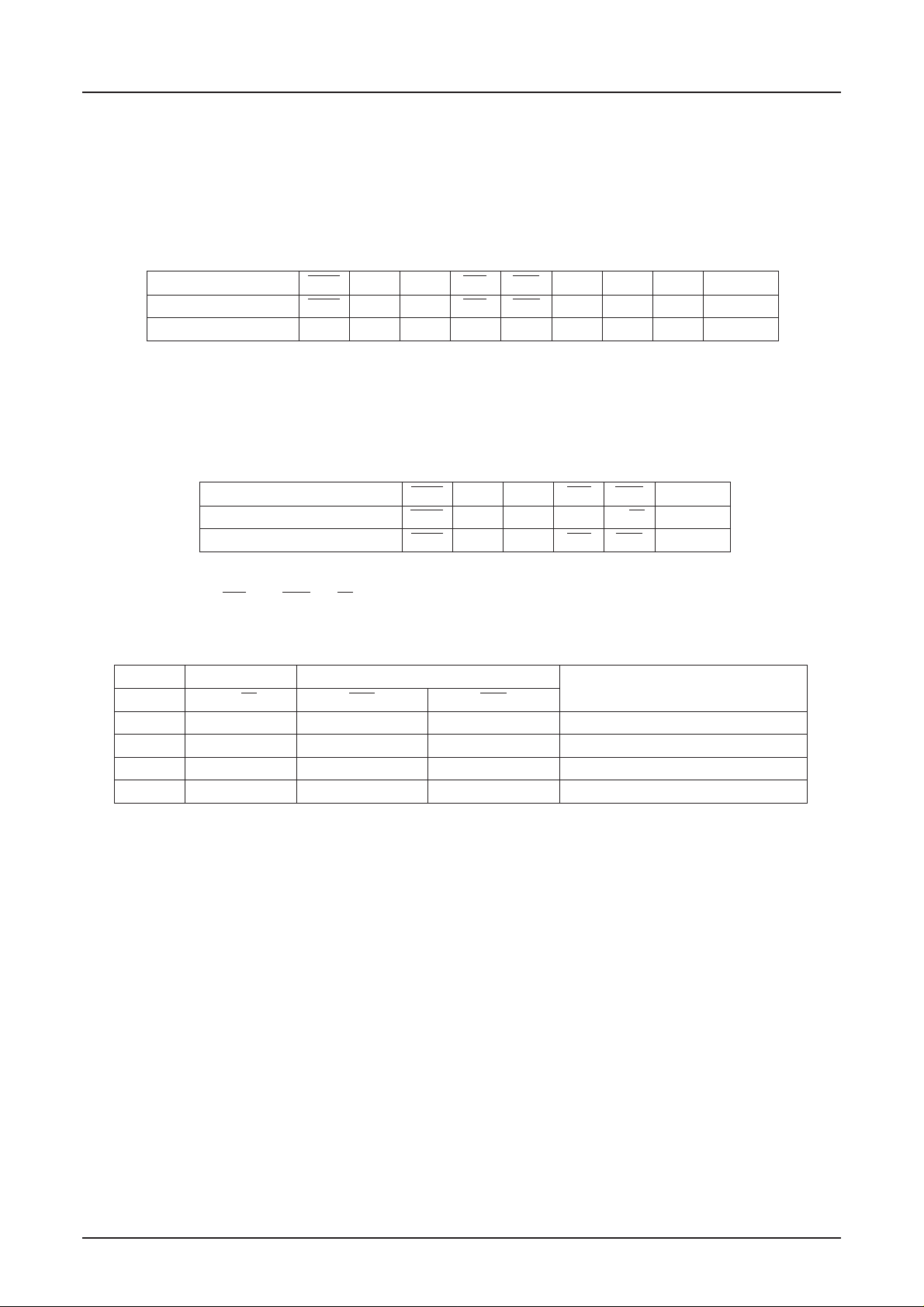
Series Specifications
Bare chip
Product Name Duty Bias SEG Dr COM Dr V
S1D15605D00B
S1D15605D11B
S1D15605D11E
S1D15605D01B
S1D15605D02B
S1D15606D00B
S1D15606D01B
S1D15606D02B
S1D15606D11B
S1D15607D00B
S1D15607D01B
S1D15607D02B
S1D15607D11B
S1D15608D00B
S1D15609D00B
TCP
*
*
*
*
*
*
*
*
*
*
*
*
*
*
*
1/65 1/9, 1/7 132 65 –0.05%/°C 625 µm
1/65 1/9, 1/7 132 65 –0.05%/°C 625 µm
1/65 1/9, 1/7 132 65 –0.05%/°C 300 µm
1/65 1/9, 1/7 132 65 –0.2%/°C 625 µm
1/65 1/9, 1/7 132 65 External Input 625 µm
1/49 1/8, 1/6 132 49 –0.05%/°C 625 µm
1/49 1/8, 1/6 132 49 –0.2%/°C 625 µm
1/49 1/8, 1/6 132 49 External Input 625 µm
1/49 1/8, 1/6 132 49 –0.05%/°C 625 µm
1/33 1/6, 1/5 132 33 –0.05%/°C 625 µm
1/33 1/6, 1/5 132 33 –0.2%/°C 625 µm
1/33 1/6, 1/5 132 33 External Input 625 µm
1/33 1/6, 1/5 132 33 –0.05%/°C 625 µm
1/55 1/8, 1/6 132 55 –0.05%/°C 625 µm
1/53 1/8, 1/6 132 53 –0.05%/°C 625 µm
REG Temperature Chip
Gradient Thickness
Product Name Duty Bias SEG Dr COM Dr VREG Temperature Gradient
S1D15605T00
S1D15606T00
S1D15607T00
Product name of custom TCP can be coped with specially.
**
**
**
1/65 1/9, 1/7 132 65 –0.05%/°C
1/49 1/8, 1/6 132 49 –0.05%/°C
1/33 1/6, 1/5 132 33 –0.05%/°C
8–2 EPSON Rev. 2.4a
Page 5
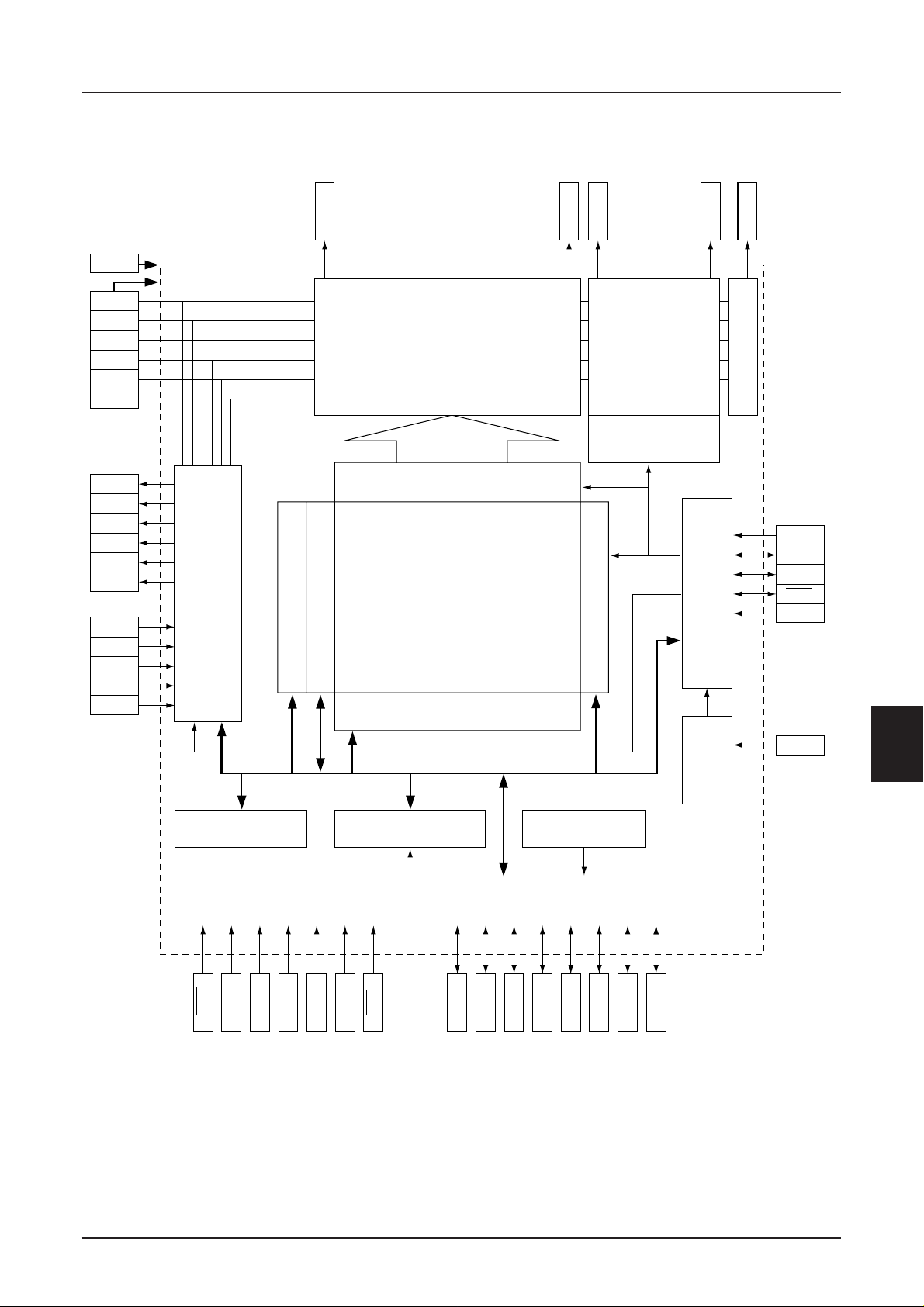
3. BLOCK DIAGRAM
Example: S1D15605
VSS
VDD
V1
V2
V3
V4
V5
*****
• • • • • • • • • • • • • • • • • • • • • • • • • • • • • • • • • • •
SEG0
COM0
SEG131
COM DriversSEG Drivers
Shift register
S1D15605 Series
COMS
COM63
COMS
CAP1+
CAP1–
CAP2+
CAP2–
CAP3+
VOUT
VSS2
VR
VRS
IRS
HPM
Power
supply
circuit
Bus holder
Display data latch circuit
I/O buffer
Page address circuit
Column address circuit
MPU interface
Display data RAM
132 x 65
Line address circuit
StatusCommand decoder
FRS
FR
CL
DOF
M/S
Display timing generation circuit
CLS
circuit
Oscillator
CS1
CS2
A0
RD (E)
P/S
WR (R/W)
RES
D7 (SI)
D5
D6 (SCL)
D4
D3
D2
D1
D0
Rev. 2.4a EPSON 8–3
Page 6

S1D15605 Series
4. PAD
Pad Layout
99 1
100
S1D15605 Series
(0, 0)
Die No.
D1565D
0B
309
134
275
135 274
Chip Size 10.82 mm × 2.81 mm
Chip Thickness 0.625 mm
Bump Pitch 71 µm (Min.)
Bump Size PAD No. 1~24 85 µm × 85 µm
PAD No. 25~82 64 µm × 85 µm
PAD No. 83~99 85 µm × 85 µm
PAD No. 100 85 µm × 73 µm
PAD No. 101~133 85 µm × 47 µm
PAD No. 134 85 µm × 73 µm
PAD No. 135 73 µm × 85 µm
PAD No. 136~273 47 µm × 85 µm
PAD No. 274 73 µm × 85 µm
PAD No. 275 86 µm × 73 µm
PAD No. 276~308 85 µm × 47 µm
PAD No. 309 85 µm × 73 µm
Bump Height 17 µm (Typ.)
8–4 EPSON Rev. 2.4a
Page 7
S1D15605 Series
S1D15605
PAD PIN
No. Name
Pad Center Coordinates
*****
XY
1 (NC) 4973 1246
2 FRS 4853
3 FR 4734
4 CL 4614
5 DOF 4494
6 TEST0 4375
7V
SS 4255
8 CS1 4136
9 CS2 4016
10 VDD 3896
11 RES 3777
12 A0 3657
13 V
SS 3538
14 WR, R/W 3418
15 RD, E 3298
16 V
DD 3179
17 D0 3059
18 D1 2940
19 D2 2820
20 D3 2700
21 D4 2581
22 D5 2461
23 D6, SCL 2342
24 D7, SI 2222
25 (NC) 2119
26 V
DD 2030
27 VDD 1941
28 VDD 1852
29 V
DD 1763
30 VSS 1674
31 VSS 1585
32 VSS 1496
33 V
SS2 1407
34 VSS2 1318
35 VSS2 1229
36 VSS2 1140
37 (NC) 1051
38 V
OUT 962
39 VOUT 873
40 CAP3– 784
PAD PIN
No. Name
XY
41 CAP3– 695 1246
42 (NC) 605
43 CAP1+ 516
44 CAP1+ 427
45 CAP1– 338
46 CAP1– 249
47 CAP2– 160
48 CAP2– 71
49 CAP2+ –18
50 CAP2+ –107
51 V
SS –196
52 VSS –285
53 V
RS –374
54 VRS –463
55 VDD –552
56 VDD –641
57 V1 –730
58 V
1 –819
59 V2 –908
60 V2 –997
61 (NC) –1086
62 V
3 –1176
63 V3 –1265
64 V4 –1354
65 V4 –1443
66 V
5 –1532
67 V5 –1621
68 (NC) –1710
69 VR –1799
70 VR –1888
71 V
DD –1977
72 VDD –2066
73 TEST1 –2155
74 TEST1 –2244
75 TEST2 –2333
76 TEST2 –2422
77 (NC) –2511
78 TEST3 –2600
79 TEST3 –2689
80 TEST4 –2778
Units: µm
PAD PIN
No. Name
XY
81 TEST4 –2867 1246
82 (NC) –2957
83 V
DD –3059
84 M/S –3179
85 CLS –3298
86 VSS –3418
87 C86 –3538
88 P/S –3657
89 V
DD –3777
90 HPM –3896
91 V
SS –4016
92 IRS –4136
93 VDD –4255
94 TEST5 –4375
95 TEST6 –4494
96 TEST7 –4614
97 TEST8 –4734
98 TEST9 –4853
99 (NC) –4973
100 (NC) –5252 1248
101 COM31 1163
102 COM30 1090
103 COM29 1017
104 COM28 945
105 COM27 872
106 COM26 799
107 COM25 727
108 COM24 654
109 COM23 581
110 COM22 509
111 COM21 436
112 COM20 363
113 COM19 291
114 COM18 218
115 COM17 145
116 COM16 73
117 COM15 0
118 COM14 –73
119 COM13 –145
120 COM12 –218
Rev. 2.4a EPSON 8–5
Page 8
S1D15605 Series
Units: µm
PAD PIN
No. Name
121 COM11 –5252 –291
122 COM10 –363
123 COM9 –436
124 COM8 –509
125 COM7 –581
126 COM6 –654
127 COM5 –727
128 COM4 –800
129 COM3 –872
130 COM2 –945
131 COM1 –1018
132 COM0 –1090
133 COMS –1163
134 (NC) –1248
135 (NC) –5009 –1246
136 (NC) –4924
137 (NC) –4853
138 (NC) –4781
139 SEG0 –4709
140 SEG1 –4637
141 SEG2 –4565
142 SEG3 –4493
143 SEG4 –4421
144 SEG5 –4349
145 SEG6 –4277
146 SEG7 –4206
147 SEG8 –4134
148 SEG9 –4062
149 SEG10 –3990
150 SEG11 –3918
151 SEG12 –3846
152 SEG13 –3774
153 SEG14 –3702
154 SEG15 –3630
155 SEG16 –3559
156 SEG17 –3487
157 SEG18 –3415
158 SEG19 –3343
159 SEG20 –3271
160 SEG21 –3199
XY
PAD PIN
No. Name
161 SEG22 –3127 –1246
162 SEG23 –3055
163 SEG24 –2983
164 SEG25 –2912
165 SEG26 –2840
166 SEG27 –2768
167 SEG28 –2696
168 SEG29 –2624
169 SEG30 –2552
170 SEG31 –2480
171 SEG32 –2408
172 SEG33 –2336
173 SEG34 –2265
174 SEG35 –2193
175 SEG36 –2121
176 SEG37 –2049
177 SEG38 –1977
178 SEG39 –1905
179 SEG40 –1833
180 SEG41 –1761
181 SEG42 –1689
182 SEG43 –1618
183 SEG44 –1546
184 SEG45 –1474
185 SEG46 –1402
186 SEG47 –1330
187 SEG48 –1258
188 SEG49 –1186
189 SEG50 –1114
190 SEG51 –1042
191 SEG52 –971
192 SEG53 –899
193 SEG54 –827
194 SEG55 –755
195 SEG56 –683
196 SEG57 –611
197 SEG58 –539
198 SEG59 –467
199 SEG60 –395
200 SEG61 –324
XY
PAD PIN
No. Name
201 SEG62 –252 –1246
202 SEG63 –180
203 SEG64 –108
204 SEG65 –36
205 SEG66 36
206 SEG67 108
207 SEG68 180
208 SEG69 252
209 SEG70 324
210 SEG71 395
211 SEG72 467
212 SEG73 539
213 SEG74 611
214 SEG75 683
215 SEG76 755
216 SEG77 827
217 SEG78 899
218 SEG79 971
219 SEG80 1042
220 SEG81 1114
221 SEG82 1186
222 SEG83 1258
223 SEG84 1330
224 SEG85 1402
225 SEG86 1474
226 SEG87 1546
227 SEG88 1618
228 SEG89 1689
229 SEG90 1761
230 SEG91 1833
231 SEG92 1905
232 SEG93 1977
233 SEG94 2049
234 SEG95 2121
235 SEG96 2193
236 SEG97 2265
237 SEG98 2336
238 SEG99 2408
239 SEG100 2480
240 SEG101 2552
XY
8–6 EPSON Rev. 2.4a
Page 9

S1D15605 Series
Units: µm
PAD PIN
No. Name
241 SEG102 2624 –1246
242 SEG103 2696
243 SEG104 2768
244 SEG105 2840
245 SEG106 2912
246 SEG107 2983
247 SEG108 3055
248 SEG109 3127
249 SEG110 3199
250 SEG111 3271
251 SEG112 3343
252 SEG113 3415
253 SEG114 3487
254 SEG115 3558
255 SEG116 3630
256 SEG117 3702
257 SEG118 3774
258 SEG119 3846
259 SEG120 3918
260 SEG121 3990
261 SEG122 4062
262 SEG123 4134
263 SEG124 4206
264 SEG125 4277
265 SEG126 4349
266 SEG127 4421
267 SEG128 4493
268 SEG129 4565
269 SEG130 4637
270 SEG131 4709
271 (NC) 4781
272 (NC) 4853
273 (NC) 4924
274 (NC) 5009
275 (NC) 5252 –1248
276 COM32 –1163
277 COM33 –1090
278 COM34 –1018
279 COM35 –945
280 COM36 –872
XY
PAD PIN
No. Name
281 COM37 5252 –800
282 COM38 –727
283 COM39 –654
284 COM40 –581
285 COM41 –509
286 COM42 –436
287 COM43 –363
288 COM44 –291
289 COM45 –218
290 COM46 –145
291 COM47 –73
292 COM48 0
293 COM49 73
294 COM50 145
295 COM51 218
296 COM52 291
297 COM53 363
298 COM54 436
299 COM55 509
300 COM56 581
301 COM57 654
302 COM58 727
303 COM59 799
304 COM60 872
305 COM61 945
306 COM62 1017
307 COM63 1090
308 COMS 1163
309 (NC) 1248
XY
Rev. 2.4a EPSON 8–7
Page 10
S1D15605 Series
S1D15606
PAD PIN
No. Name
Pad Center Coordinates
*****
XY
1 (NC) 4973 1246
2 FRS 4853
3 FR 4734
4 CL 4614
5 DOF 4494
6 TEST0 4375
7V
SS 4255
8 CS1 4136
9 CS2 4016
10 VDD 3896
11 RES 3777
12 A0 3657
13 V
SS 3538
14 WR, R/W 3418
15 RD, E 3298
16 V
DD 3179
17 D0 3059
18 D1 2940
19 D2 2820
20 D3 2700
21 D4 2581
22 D5 2461
23 D6, SCL 2342
24 D7, SI 2222
25 (NC) 2119
26 V
DD 2030
27 VDD 1941
28 VDD 1852
29 V
DD 1763
30 VSS 1674
31 VSS 1585
32 VSS 1496
33 V
SS2 1407
34 VSS2 1318
35 VSS2 1229
36 VSS2 1140
37 (NC) 1051
38 V
OUT 962
39 VOUT 873
40 CAP3– 784
PAD PIN
No. Name
XY
41 CAP3– 695 1246
42 (NC) 605
43 CAP1+ 516
44 CAP1+ 427
45 CAP1– 338
46 CAP1– 249
47 CAP2– 160
48 CAP2– 71
49 CAP2+ –18
50 CAP2+ –107
51 V
SS –196
52 VSS –285
53 V
RS –374
54 VRS –463
55 VDD –552
56 VDD –641
57 V1 –730
58 V
1 –819
59 V2 –908
60 V2 –997
61 (NC) –1086
62 V
3 –1176
63 V3 –1265
64 V4 –1354
65 V4 –1443
66 V
5 –1532
67 V5 –1621
68 (NC) –1710
69 VR –1799
70 VR –1888
71 V
DD –1977
72 VDD –2066
73 TEST1 –2155
74 TEST1 –2244
75 TEST2 –2333
76 TEST2 –2422
77 (NC) –2511
78 TEST3 –2600
79 TEST3 –2689
80 TEST4 –2778
Units: µm
PAD PIN
No. Name
XY
81 TEST4 –2867 1246
82 (NC) –2957
83 V
DD –3059
84 M/S –3179
85 CLS –3298
86 VSS –3418
87 C86 –3538
88 P/S –3657
89 V
DD –3777
90 HPM –3896
91 V
SS –4016
92 IRS –4136
93 VDD –4255
94 TEST5 –4375
95 TEST6 –4494
96 TEST7 –4614
97 TEST8 –4734
98 TEST9 –4853
99 (NC) –4973
100 (NC) –5252 1248
101 (NC) 1163
102 (NC) 1090
103 COM23 1017
104 (NC) 945
105 COM22 872
106 (NC) 799
107 COM21 727
108 COM20 654
109 COM19 581
110 COM18 509
111 COM17 436
112 COM16 363
113 COM15 291
114 COM14 218
115 COM13 145
116 COM12 73
117 COM11 0
118 COM10 –73
119 COM9 –145
120 COM8 –218
8–8 EPSON Rev. 2.4a
Page 11

S1D15605 Series
Units: µm
PAD PIN
No. Name
121 COM7 –5252 –291
122 COM6 –363
123 COM5 –436
124 COM4 –509
125 COM3 –581
126 COM2 –654
127 COM1 –727
128 (NC) –800
129 COM0 –872
130 (NC) –945
131 COMS –1018
132 (NC) –1090
133 (NC) –1163
134 (NC) –1248
135 (NC) –5009 –1246
136 (NC) –4924
137 (NC) –4853
138 (NC) –4781
139 SEG0 –4709
140 SEG1 –4637
141 SEG2 –4565
142 SEG3 –4493
143 SEG4 –4421
144 SEG5 –4349
145 SEG6 –4277
146 SEG7 –4206
147 SEG8 –4134
148 SEG9 –4062
149 SEG10 –3990
150 SEG11 –3918
151 SEG12 –3846
152 SEG13 –3774
153 SEG14 –3702
154 SEG15 –3630
155 SEG16 –3559
156 SEG17 –3487
157 SEG18 –3415
158 SEG19 –3343
159 SEG20 –3271
160 SEG21 –3199
XY
PAD PIN
No. Name
161 SEG22 –3127 –1246
162 SEG23 –3055
163 SEG24 –2983
164 SEG25 –2912
165 SEG26 –2840
166 SEG27 –2768
167 SEG28 –2696
168 SEG29 –2624
169 SEG30 –2552
170 SEG31 –2480
171 SEG32 –2408
172 SEG33 –2336
173 SEG34 –2265
174 SEG35 –2193
175 SEG36 –2121
176 SEG37 –2049
177 SEG38 –1977
178 SEG39 –1905
179 SEG40 –1833
180 SEG41 –1761
181 SEG42 –1689
182 SEG43 –1618
183 SEG44 –1546
184 SEG45 –1474
185 SEG46 –1402
186 SEG47 –1330
187 SEG48 –1258
188 SEG49 –1186
189 SEG50 –1114
190 SEG51 –1042
191 SEG52 –971
192 SEG53 –899
193 SEG54 –827
194 SEG55 –755
195 SEG56 –683
196 SEG57 –611
197 SEG58 –539
198 SEG59 –467
199 SEG60 –395
200 SEG61 –324
XY
PAD PIN
No. Name
201 SEG62 –252 –1246
202 SEG63 –180
203 SEG64 –108
204 SEG65 –36
205 SEG66 36
206 SEG67 108
207 SEG68 180
208 SEG69 252
209 SEG70 324
210 SEG71 395
211 SEG72 467
212 SEG73 539
213 SEG74 611
214 SEG75 683
215 SEG76 755
216 SEG77 827
217 SEG78 899
218 SEG79 971
219 SEG80 1042
220 SEG81 1114
221 SEG82 1186
222 SEG83 1258
223 SEG84 1330
224 SEG85 1402
225 SEG86 1474
226 SEG87 1546
227 SEG88 1618
228 SEG89 1689
229 SEG90 1761
230 SEG91 1833
231 SEG92 1905
232 SEG93 1977
233 SEG94 2049
234 SEG95 2121
235 SEG96 2193
236 SEG97 2265
237 SEG98 2336
238 SEG99 2408
239 SEG100 2480
240 SEG101 2552
XY
Rev. 2.4a EPSON 8–9
Page 12
S1D15605 Series
Units: µm
PAD PIN
No. Name
241 SEG102 2624 –1246
242 SEG103 2696
243 SEG104 2768
244 SEG105 2840
245 SEG106 2912
246 SEG107 2983
247 SEG108 3055
248 SEG109 3127
249 SEG110 3199
250 SEG111 3271
251 SEG112 3343
252 SEG113 3415
253 SEG114 3487
254 SEG115 3558
255 SEG116 3630
256 SEG117 3702
257 SEG118 3774
258 SEG119 3846
259 SEG120 3918
260 SEG121 3990
261 SEG122 4062
262 SEG123 4134
263 SEG124 4206
264 SEG125 4277
265 SEG126 4349
266 SEG127 4421
267 SEG128 4493
268 SEG129 4565
269 SEG130 4637
270 SEG131 4709
271 (NC) 4781
272 (NC) 4853
273 (NC) 4924
274 (NC) 5009
275 (NC) 5252 –1248
276 (NC) –1163
277 (NC) –1090
278 COM24 –1018
279 (NC) –945
280 COM25 –872
XY
PAD PIN
No. Name
281 (NC) 5252 –800
282 COM26 –727
283 COM27 –654
284 COM28 –581
285 COM29 –509
286 COM30 –436
287 COM31 –363
288 COM32 –291
289 COM33 –218
290 COM34 –145
291 COM35 –73
292 COM36 0
293 COM37 73
294 COM38 145
295 COM39 218
296 COM40 291
297 COM41 363
298 COM42 436
299 COM43 509
300 COM44 581
301 COM45 654
302 COM46 727
303 (NC) 799
304 COM47 872
305 (NC) 945
306 COMS 1017
307 (NC) 1090
308 (NC) 1163
309 (NC) 1248
XY
8–10 EPSON Rev. 2.4a
Page 13

S1D15605 Series
S1D15607
PAD PIN
No. Name
Pad Center Coordinates
*****
XY
1 (NC) 4973 1246
2 FRS 4853
3 FR 4734
4 CL 4614
5 DOF 4494
6 TEST0 4375
7V
SS 4255
8 CS1 4136
9 CS2 4016
10 V
DD 3896
11 RES 3777
12 A0 3657
13 V
SS 3538
14 WR, R/W 3418
15 RD, E 3298
16 V
DD 3179
17 D0 3059
18 D1 2940
19 D2 2820
20 D3 2700
21 D4 2581
22 D5 2461
23 D6, SCL 2342
24 D7, SI 2222
25 (NC) 2119
26 V
DD 2030
27 VDD 1941
28 VDD 1852
29 V
DD 1763
30 VSS 1674
31 VSS 1585
32 VSS 1496
33 VSS2 1407
34 V
SS2 1318
35 VSS2 1229
36 VSS2 1140
37 (NC) 1051
38 V
OUT 962
39 VOUT 873
40 CAP3– 784
PAD PIN
No. Name
XY
41 CAP3– 695 1246
42 (NC) 605
43 CAP1+ 516
44 CAP1+ 427
45 CAP1– 338
46 CAP1– 249
47 CAP2– 160
48 CAP2– 71
49 CAP2+ –18
50 CAP2+ –107
51 V
52 V
SS –196
SS –285
53 VRS –374
54 VRS –463
55 VDD –552
56 V
DD –641
57 V1 –730
58 V1 –819
59 V2 –908
60 V2 –997
61 (NC) –1086
62 V
3 –1176
63 V3 –1265
64 V4 –1354
65 V
4 –1443
66 V5 –1532
67 V5 –1621
68 (NC) –1710
69 V
R –1799
70 VR –1888
71 VDD –1977
72 VDD –2066
73 TEST1 –2155
74 TEST1 –2244
75 TEST2 –2333
76 TEST2 –2422
77 (NC) –2511
78 TEST3 –2600
79 TEST3 –2689
80 TEST4 –2778
Units: µm
PAD PIN
No. Name
XY
81 TEST4 –2867 1246
82 (NC) –2957
83 V
DD –3059
84 M/S –3179
85 CLS –3298
86 VSS –3418
87 C86 –3538
88 P/S –3657
89 V
DD –3777
90 HPM –3896
91 VSS –4016
92 IRS –4136
93 V
DD –4255
94 TEST5 –4375
95 TEST6 –4494
96 TEST7 –4614
97 TEST8 –4734
98 TEST9 –4853
99 (NC) –4973
100 (NC) –5252 1248
101 COM15 1163
102 COM15 1090
103 COM14 1017
104 COM14 945
105 COM13 872
106 COM13 799
107 COM12 727
108 COM12 654
109 COM11 581
110 COM11 509
111 COM10 436
112 COM10 363
113 COM9 291
114 COM9 218
115 COM8 145
116 COM8 73
117 COM7 0
118 COM7 –73
119 COM6 –145
120 COM6 –218
Rev. 2.4a EPSON 8–11
Page 14
S1D15605 Series
Units: µm
PAD PIN
No. Name
121 COM5 –5252 –291
122 COM5 –363
123 COM4 –436
124 COM4 –509
125 COM3 –581
126 COM3 –654
127 COM2 –727
128 COM2 –800
129 COM1 –872
130 COM1 –945
131 COM0 –1018
132 COM0 –1090
133 COMS –1163
134 (NC) –1248
135 (NC) –5009 –1246
136 (NC) –4924
137 (NC) –4853
138 (NC) –4781
139 SEG0 –4709
140 SEG1 –4637
141 SEG2 –4565
142 SEG3 –4493
143 SEG4 –4421
144 SEG5 –4349
145 SEG6 –4277
146 SEG7 –4206
147 SEG8 –4134
148 SEG9 –4062
149 SEG10 –3990
150 SEG11 –3918
151 SEG12 –3846
152 SEG13 –3774
153 SEG14 –3702
154 SEG15 –3630
155 SEG16 –3559
156 SEG17 –3487
157 SEG18 –3415
158 SEG19 –3343
159 SEG20 –3271
160 SEG21 –3199
XY
PAD PIN
No. Name
161 SEG22 –3127 –1246
162 SEG23 –3055
163 SEG24 –2983
164 SEG25 –2912
165 SEG26 –2840
166 SEG27 –2768
167 SEG28 –2696
168 SEG29 –2624
169 SEG30 –2552
170 SEG31 –2480
171 SEG32 –2408
172 SEG33 –2336
173 SEG34 –2265
174 SEG35 –2193
175 SEG36 –2121
176 SEG37 –2049
177 SEG38 –1977
178 SEG39 –1905
179 SEG40 –1833
180 SEG41 –1761
181 SEG42 –1689
182 SEG43 –1618
183 SEG44 –1546
184 SEG45 –1474
185 SEG46 –1402
186 SEG47 –1330
187 SEG48 –1258
188 SEG49 –1186
189 SEG50 –1114
190 SEG51 –1042
191 SEG52 –971
192 SEG53 –899
193 SEG54 –827
194 SEG55 –755
195 SEG56 –683
196 SEG57 –611
197 SEG58 –539
198 SEG59 –467
199 SEG60 –395
200 SEG61 –324
XY
PAD PIN
No. Name
201 SEG62 –252 –1246
202 SEG63 –180
203 SEG64 –108
204 SEG65 –36
205 SEG66 36
206 SEG67 108
207 SEG68 180
208 SEG69 252
209 SEG70 324
210 SEG71 395
211 SEG72 467
212 SEG73 539
213 SEG74 611
214 SEG75 683
215 SEG76 755
216 SEG77 827
217 SEG78 899
218 SEG79 971
219 SEG80 1042
220 SEG81 1114
221 SEG82 1186
222 SEG83 1258
223 SEG84 1330
224 SEG85 1402
225 SEG86 1474
226 SEG87 1546
227 SEG88 1618
228 SEG89 1689
229 SEG90 1761
230 SEG91 1833
231 SEG92 1905
232 SEG93 1977
233 SEG94 2049
234 SEG95 2121
235 SEG96 2193
236 SEG97 2265
237 SEG98 2336
238 SEG99 2408
239 SEG100 2480
240 SEG101 2552
XY
8–12 EPSON Rev. 2.4a
Page 15

S1D15605 Series
Units: µm
PAD PIN
No. Name
241 SEG102 2624 –1246
242 SEG103 2696
243 SEG104 2768
244 SEG105 2840
245 SEG106 2912
246 SEG107 2983
247 SEG108 3055
248 SEG109 3127
249 SEG110 3199
250 SEG111 3271
251 SEG112 3343
252 SEG113 3415
253 SEG114 3487
254 SEG115 3558
255 SEG116 3630
256 SEG117 3702
257 SEG118 3774
258 SEG119 3846
259 SEG120 3918
260 SEG121 3990
261 SEG122 4062
262 SEG123 4134
263 SEG124 4206
264 SEG125 4277
265 SEG126 4349
266 SEG127 4421
267 SEG128 4493
268 SEG129 4565
269 SEG130 4637
270 SEG131 4709
271 (NC) 4781
272 (NC) 4853
273 (NC) 4924
274 (NC) 5009
275 (NC) 5252 –1248
276 COM16 –1163
277 COM16 –1090
278 COM17 –1018
279 COM17 –945
280 COM18 –872
XY
PAD PIN
No. Name
281 COM18 5252 –800
282 COM19 –727
283 COM19 –654
284 COM20 –581
285 COM20 –509
286 COM21 –436
287 COM21 –363
288 COM22 –291
289 COM22 –218
290 COM23 –145
291 COM23 –73
292 COM24 0
293 COM24 73
294 COM25 145
295 COM25 218
296 COM26 291
297 COM26 363
298 COM27 436
299 COM27 509
300 COM28 581
301 COM28 654
302 COM29 727
303 COM29 799
304 COM30 872
305 COM30 945
306 COM31 1017
307 COM31 1090
308 COMS 1163
309 (NC) 1248
XY
Rev. 2.4a EPSON 8–13
Page 16
S1D15605 Series
S1D15608
PAD PIN
No. Name
Pad Center Coordinates
*****
XY
1 (NC) 4973 1246
2 FRS 4853
3 FR 4734
4 CL 4614
5 DOF 4494
6 TEST0 4375
7V
SS 4255
8 CS1 4136
9 CS2 4016
10 V
DD 3896
11 RES 3777
12 A0 3657
13 V
SS 3538
14 WR, R/W 3418
15 RD, E 3298
16 V
DD 3179
17 D0 3059
18 D1 2940
19 D2 2820
20 D3 2700
21 D4 2581
22 D5 2461
23 D6, SCL 2342
24 D7, SI 2222
25 (NC) 2119
26 V
DD 2030
27 VDD 1941
28 VDD 1852
29 V
DD 1763
30 VSS 1674
31 VSS 1585
32 VSS 1496
33 VSS2 1407
34 V
SS2 1318
35 VSS2 1229
36 VSS2 1140
37 (NC) 1051
38 V
OUT 962
39 VOUT 873
40 CAP3– 784
PAD PIN
No. Name
XY
41 CAP3– 695 1246
42 (NC) 605
43 CAP1+ 516
44 CAP1+ 427
45 CAP1– 338
46 CAP1– 249
47 CAP2– 160
48 CAP2– 71
49 CAP2+ –18
50 CAP2+ –107
51 V
SS –196
52 VSS –285
53 VRS –374
54 VRS –463
55 V
DD –552
56 VDD –641
57 V1 –730
58 V1 –819
59 V
2 –908
60 V2 –997
61 (NC) –1086
62 V3 –1176
63 V3 –1265
64 V
4 –1354
65 V4 –1443
66 V5 –1532
67 V5 –1621
68 (NC) –1710
69 V
R –1799
70 VR –1888
71 VDD –1977
72 V
DD –2066
73 TEST1 –2155
74 TEST1 –2244
75 TEST2 –2333
76 TEST2 –2422
77 (NC) –2511
78 TEST3 –2600
79 TEST3 –2689
80 TEST4 –2778
Units: µm
PAD PIN
No. Name
XY
81 TEST4 –2867 1246
82 (NC) –2957
83 V
DD –3059
84 M/S –3179
85 CLS –3298
86 V
SS –3418
87 C86 –3538
88 P/S –3657
89 VDD –3777
90 HPM –3896
91 V
SS –4016
92 IRS –4136
93 VDD –4255
94 TEST5 –4375
95 TEST6 –4494
96 TEST7 –4614
97 TEST8 –4734
98 TEST9 –4853
99 (NC) –4973
100 (NC) –5252 1248
101 (NC) 1163
102 COM26 1090
103 (NC) 1017
104 COM25 945
105 COM25 872
106 COM23 799
107 COM22 727
108 COM21 654
109 COM20 581
110 COM19 509
111 COM18 436
112 COM17 363
113 COM16 291
114 COM15 218
115 COM14 145
116 COM13 73
117 COM12 0
118 COM11 –73
119 COM10 –145
120 COM9 –218
8–14 EPSON Rev. 2.4a
Page 17

S1D15605 Series
Units: µm
PAD PIN
No. Name
121 COM8 –5252 –291
122 COM7 –363
123 COM6 –436
124 COM5 –509
125 COM4 –581
126 COM3 –654
127 COM2 –727
128 COM1 –800
129 (NC) –872
130 COM0 –945
131 (NC) –1018
132 COMS –1090
133 (NC) –1163
134 (NC) –1248
135 (NC) –5009 –1246
136 (NC) –4924
137 (NC) –4853
138 (NC) –4781
139 SEG0 –4709
140 SEG1 –4637
141 SEG2 –4565
142 SEG3 –4493
143 SEG4 –4421
144 SEG5 –4349
145 SEG6 –4277
146 SEG7 –4206
147 SEG8 –4134
148 SEG9 –4062
149 SEG10 –3990
150 SEG11 –3918
151 SEG12 –3846
152 SEG13 –3774
153 SEG14 –3702
154 SEG15 –3630
155 SEG16 –3559
156 SEG17 –3487
157 SEG18 –3415
158 SEG19 –3343
159 SEG20 –3271
160 SEG21 –3199
XY
PAD PIN
No. Name
161 SEG22 –3127 –1246
162 SEG23 –3055
163 SEG24 –2983
164 SEG25 –2912
165 SEG26 –2840
166 SEG27 –2768
167 SEG28 –2696
168 SEG29 –2624
169 SEG30 –2552
170 SEG31 –2480
171 SEG32 –2408
172 SEG33 –2336
173 SEG34 –2265
174 SEG35 –2193
175 SEG36 –2121
176 SEG37 –2049
177 SEG38 –1977
178 SEG39 –1905
179 SEG40 –1833
180 SEG41 –1761
181 SEG42 –1689
182 SEG43 –1618
183 SEG44 –1546
184 SEG45 –1474
185 SEG46 –1402
186 SEG47 –1330
187 SEG48 –1258
188 SEG49 –1186
189 SEG50 –1114
190 SEG51 –1042
191 SEG52 –971
192 SEG53 –899
193 SEG54 –827
194 SEG55 –755
195 SEG56 –683
196 SEG57 –611
197 SEG58 –539
198 SEG59 –467
199 SEG60 –395
200 SEG61 –324
XY
PAD PIN
No. Name
201 SEG62 –252 –1246
202 SEG63 –180
203 SEG64 –108
204 SEG65 –36
205 SEG66 36
206 SEG67 108
207 SEG68 180
208 SEG69 252
209 SEG70 324
210 SEG71 395
211 SEG72 467
212 SEG73 539
213 SEG74 611
214 SEG75 683
215 SEG76 755
216 SEG77 827
217 SEG78 899
218 SEG79 971
219 SEG80 1042
220 SEG81 1114
221 SEG82 1186
222 SEG83 1258
223 SEG84 1330
224 SEG85 1402
225 SEG86 1474
226 SEG87 1546
227 SEG88 1618
228 SEG89 1689
229 SEG90 1761
230 SEG91 1833
231 SEG92 1905
232 SEG93 1977
233 SEG94 2049
234 SEG95 2121
235 SEG96 2193
236 SEG97 2265
237 SEG98 2336
238 SEG99 2408
239 SEG100 2480
240 SEG101 2552
XY
Rev. 2.4a EPSON 8–15
Page 18
S1D15605 Series
Units: µm
PAD PIN
No. Name
241 SEG102 2624 –1246
242 SEG103 2696
243 SEG104 2768
244 SEG105 2840
245 SEG106 2912
246 SEG107 2983
247 SEG108 3055
248 SEG109 3127
249 SEG110 3199
250 SEG111 3271
251 SEG112 3343
252 SEG113 3415
253 SEG114 3487
254 SEG115 3558
255 SEG116 3630
256 SEG117 3702
257 SEG118 3774
258 SEG119 3846
259 SEG120 3918
260 SEG121 3990
261 SEG122 4062
262 SEG123 4134
263 SEG124 4206
264 SEG125 4277
265 SEG126 4349
266 SEG127 4421
267 SEG128 4493
268 SEG129 4565
269 SEG130 4637
270 SEG131 4709
271 (NC) 4781
272 (NC) 4853
273 (NC) 4924
274 (NC) 5009
275 (NC) 5252 –1248
276 (NC) –1163
277 COM27 –1090
278 (NC) –1018
279 COM28 –945
280 (NC) –872
XY
PAD PIN
No. Name
281 COM29 5252 –800
282 COM30 –727
283 COM31 –654
284 COM32 –581
285 COM33 –509
286 COM34 –436
287 COM35 –363
288 COM36 –291
289 COM37 –218
290 COM38 –145
291 COM39 –73
292 COM40 0
293 COM41 73
294 COM42 145
295 COM43 218
296 COM44 291
297 COM45 363
298 COM46 436
299 COM47 509
300 COM48 581
301 COM48 654
302 COM50 727
303 COM51 799
304 COM52 872
305 COM53 945
306 (NC) 1017
307 COMS 1090
308 (NC) 1163
309 (NC) 1248
XY
8–16 EPSON Rev. 2.4a
Page 19

S1D15605 Series
S1D15609
PAD PIN
No. Name
Pad Center Coordinates
*****
XY
1 (NC) 4973 1246
2 FRS 4853
3 FR 4734
4 CL 4614
5 DOF 4494
6 TEST0 4375
7V
SS 4255
8 CS1 4136
9 CS2 4016
10 V
DD 3896
11 RES 3777
12 A0 3657
13 V
SS 3538
14 WR, R/W 3418
15 RD, E 3298
16 V
DD 3179
17 D0 3059
18 D1 2940
19 D2 2820
20 D3 2700
21 D4 2581
22 D5 2461
23 D6, SCL 2342
24 D7, SI 2222
25 (NC) 2119
26 V
DD 2030
27 VDD 1941
28 VDD 1852
29 V
DD 1763
30 VSS 1674
31 VSS 1585
32 VSS 1496
33 VSS2 1407
34 V
SS2 1318
35 VSS2 1229
36 VSS2 1140
37 (NC) 1051
38 V
OUT 962
39 VOUT 873
40 CAP3– 784
PAD PIN
No. Name
XY
41 CAP3– 695 1246
42 (NC) 605
43 CAP1+ 516
44 CAP1+ 427
45 CAP1– 338
46 CAP1– 249
47 CAP2– 160
48 CAP2– 71
49 CAP2+ –18
50 CAP2+ –107
51 V
52 V
SS –196
SS –285
53 VRS –374
54 VRS –463
55 VDD –552
56 V
DD –641
57 V1 –730
58 V1 –819
59 V2 –908
60 V2 –997
61 (NC) –1086
62 V
3 –1176
63 V3 –1265
64 V4 –1354
65 V
4 –1443
66 V5 –1532
67 V5 –1621
68 (NC) –1710
69 V
R –1799
70 VR –1888
71 VDD –1977
72 VDD –2066
73 TEST1 –2155
74 TEST1 –2244
75 TEST2 –2333
76 TEST2 –2422
77 (NC) –2511
78 TEST3 –2600
79 TEST3 –2689
80 TEST4 –2778
Units: µm
PAD PIN
No. Name
XY
81 TEST4 –2867 1246
82 (NC) –2957
83 V
DD –3059
84 M/S –3179
85 CLS –3298
86 VSS –3418
87 C86 –3538
88 P/S –3657
89 V
DD –3777
90 HPM –3896
91 VSS –4016
92 IRS –4136
93 V
DD –4255
94 TEST5 –4375
95 TEST6 –4494
96 TEST7 –4614
97 TEST8 –4734
98 TEST9 –4853
99 (NC) –4973
100 (NC) –5252 1248
101 (NC) 1163
102 COM25 1090
103 (NC) 1017
104 COM24 945
105 (NC) 872
106 COM23 799
107 COM22 727
108 COM21 654
109 COM20 581
110 COM19 509
111 COM18 436
112 COM17 363
113 COM16 291
114 COM15 218
115 COM14 145
116 COM13 73
117 COM12 0
118 COM11 –73
119 COM10 –145
120 COM9 –218
Rev. 2.4a EPSON 8–17
Page 20

S1D15605 Series
Units: µm
PAD PIN
No. Name
121 COM8 –5252 –291
122 COM7 –363
123 COM6 –436
124 COM5 –509
125 COM4 –581
126 COM3 –654
127 COM2 –727
128 COM1 –800
129 (NC) –872
130 COM0 –945
131 (NC) –1018
132 COMS –1090
133 (NC) –1163
134 (NC) –1248
135 (NC) –5009 –1246
136 (NC) –4924
137 (NC) –4853
138 (NC) –4781
139 SEG0 –4709
140 SEG1 –4637
141 SEG2 –4565
142 SEG3 –4493
143 SEG4 –4421
144 SEG5 –4349
145 SEG6 –4277
146 SEG7 –4206
147 SEG8 –4134
148 SEG9 –4062
149 SEG10 –3990
150 SEG11 –3918
151 SEG12 –3846
152 SEG13 –3774
153 SEG14 –3702
154 SEG15 –3630
155 SEG16 –3559
156 SEG17 –3487
157 SEG18 –3415
158 SEG19 –3343
159 SEG20 –3271
160 SEG21 –3199
XY
PAD PIN
No. Name
161 SEG22 –3127 –1246
162 SEG23 –3055
163 SEG24 –2983
164 SEG25 –2912
165 SEG26 –2840
166 SEG27 –2768
167 SEG28 –2696
168 SEG29 –2624
169 SEG30 –2552
170 SEG31 –2480
171 SEG32 –2408
172 SEG33 –2336
173 SEG34 –2265
174 SEG35 –2193
175 SEG36 –2121
176 SEG37 –2049
177 SEG38 –1977
178 SEG39 –1905
179 SEG40 –1833
180 SEG41 –1761
181 SEG42 –1689
182 SEG43 –1618
183 SEG44 –1546
184 SEG45 –1474
185 SEG46 –1402
186 SEG47 –1330
187 SEG48 –1258
188 SEG49 –1186
189 SEG50 –1114
190 SEG51 –1042
191 SEG52 –971
192 SEG53 –899
193 SEG54 –827
194 SEG55 –755
195 SEG56 –683
196 SEG57 –611
197 SEG58 –539
198 SEG59 –467
199 SEG60 –395
200 SEG61 –324
XY
PAD PIN
No. Name
201 SEG62 –252 –1246
202 SEG63 –180
203 SEG64 –108
204 SEG65 –36
205 SEG66 36
206 SEG67 108
207 SEG68 180
208 SEG69 252
209 SEG70 324
210 SEG71 395
211 SEG72 467
212 SEG73 539
213 SEG74 611
214 SEG75 683
215 SEG76 755
216 SEG77 827
217 SEG78 899
218 SEG79 971
219 SEG80 1042
220 SEG81 1114
221 SEG82 1186
222 SEG83 1258
223 SEG84 1330
224 SEG85 1402
225 SEG86 1474
226 SEG87 1546
227 SEG88 1618
228 SEG89 1689
229 SEG90 1761
230 SEG91 1833
231 SEG92 1905
232 SEG93 1977
233 SEG94 2049
234 SEG95 2121
235 SEG96 2193
236 SEG97 2265
237 SEG98 2336
238 SEG99 2408
239 SEG100 2480
240 SEG101 2552
XY
8–18 EPSON Rev. 2.4a
Page 21

S1D15605 Series
Units: µm
PAD PIN
No. Name
241 SEG102 2624 –1246
242 SEG103 2696
243 SEG104 2768
244 SEG105 2840
245 SEG106 2912
246 SEG107 2983
247 SEG108 3055
248 SEG109 3127
249 SEG110 3199
250 SEG111 3271
251 SEG112 3343
252 SEG113 3415
253 SEG114 3487
254 SEG115 3558
255 SEG116 3630
256 SEG117 3702
257 SEG118 3774
258 SEG119 3846
259 SEG120 3918
260 SEG121 3990
261 SEG122 4062
262 SEG123 4134
263 SEG124 4206
264 SEG125 4277
265 SEG126 4349
266 SEG127 4421
267 SEG128 4493
268 SEG129 4565
269 SEG130 4637
270 SEG131 4709
271 (NC) 4781
272 (NC) 4853
273 (NC) 4924
274 (NC) 5009
275 (NC) 5252 –1248
276 (NC) –1163
277 COM26 –1090
278 (NC) –1018
279 COM27 –945
280 (NC) –872
XY
PAD PIN
No. Name
281 COM28 5252 –800
282 COM29 –727
283 COM30 –654
284 COM31 –581
285 COM32 –509
286 COM33 –436
287 COM34 –363
288 COM35 –291
289 COM36 –218
290 COM37 –145
291 COM38 –73
292 COM39 0
293 COM40 73
294 COM41 145
295 COM42 218
296 COM43 291
297 COM44 363
298 COM45 436
299 COM46 509
300 COM47 581
301 COM48 654
302 COM49 727
303 COM50 799
304 (NC) 872
305 COM51 945
306 (NC) 1017
307 COMS 1090
308 (NC) 1163
309 (NC) 1248
XY
Rev. 2.4a EPSON 8–19
Page 22

S1D15605 Series
5. PIN DESCRIPTIONS
Power Supply Pins
Pin Name I/O Function
DD Power Shared with the MPU power supply terminal VCC.13
V
No. of
Pins
Supply
SS Power This is a 0V terminal connected to the system GND. 9
V
Supply
SS2 Power This is the reference power supply for the step-up voltage circuit for the 4
V
Supply liquid crystal drive.
RS Power This is the externally-input VREG power supply for the LCD power supply 2
V
Supply voltage regulator.
These are only enabled for the models with the VREG external input option.
1, V2, Power This is a multi-level power supply for the liquid crystal drive. The voltage 10
V
V
3, V4, Supply applied is determined by the liquid crystal cell, and is changed through the
V
5 use of a resistive voltage divided or through changing the impedance using
an op. amp. Voltage levels are determined based on V
DD, and must
maintain the relative magnitudes shown below.
V
DD (= V0) ≥ V1 ≥ V2 ≥ V3 ≥ V4 ≥ V5
Master operation: When the power supply turns ON, the internal power
supply circuits produce the V1 to V4 voltages shown below. The voltage
settings are selected using the LCD bias set command.
S1D15605
*****
S1D15606
*****
S1D15607
*****
S1D15608
*****
S1D15609
*****
V1 1/9•V5 1/7•V5 1/8•V5 1/6•V5 1/6•V5 1/5•V5 1/8•V5 1/6•V5 1/8•V5 1/6•V5
V2 2/9•V5 2/7•V5 2/8•V5 2/6•V5 2/6•V5 2/5•V5 2/8•V5 2/6•V5 2/8•V5 2/6•V5
V3 7/9•V5 5/7•V5 6/8•V5 4/6•V5 4/6•V5 3/5•V5 6/8•V5 4/6•V5 6/8•V5 4/6•V5
V4 8/9•V5 6/7•V5 7/8•V5 5/6•V5 5/6•V5 4/5•V5 7/8•V5 5/6•V5 7/6•V5 5/6•V5
LCD Power Supply Circuit Terminals
Pin Name I/O Function
CAP1+ O DC/DC voltage converter. Connect a capacitor between this terminal and 2
the CAP1- terminal.
CAP1– O DC/DC voltage converter. Connect a capacitor between this terminal and 2
the CAP1+ terminal.
CAP2+ O DC/DC voltage converter. Connect a capacitor between this terminal and 2
the CAP2- terminal.
CAP2– O DC/DC voltage converter. Connect a capacitor between this terminal and 2
the CAP2+ terminal.
CAP3– O DC/DC voltage converter. Connect a capacitor between this terminal and 2
the CAP1+ terminal.
OUT I/O DC/DC voltage converter. Connect a capacitor between this terminal and 2
V
V
SS2.
R I Output voltage regulator terminal. Provides the voltage between VDD and 2
V
V5 through a resistive voltage divider.
These are only enabled when the V
5 voltage regulator internal resistors are
not used (IRS = LOW).
These cannot be used when the V
5 voltage regulator internal resistors are
used (IRS = HIGH).
No. of
Pins
8–20 EPSON Rev. 2.4a
Page 23
System Bus Connection Terminals
S1D15605 Series
Pin Name I/O Function
D7 to D0 I/O This is an 8-bit bi-directional data bus that connects to an 8-bit or 16-bit 8
standard MPU data bus.
(SI) When the serial interface is selected (P/S = LOW), then D7 serves as the
(SCL) serial data input terminal (SI) and D6 serves as the serial clock input
terminal (SCL). At this time, D0 to D5 are set to high impedance.
When the chip select is inactive, D0 to D7 are set to high impedance.
A0 I This is connect to the least significant bit of the normal MPU address bus, 1
and it determines whether the data bits are data or a command.
A0 = HIGH: Indicates that D0 to D7 are display data.
A0 = LOW: Indicates that D0 to D7 are display control data.
RES I When RES is set to LOW, the settings are initialized. 1
The reset operation is performed by the RES signal level.
CS1 I This is the chip select signal. When CS1 = LOW and CS2 = HIGH, then the 2
CS2 chip select becomes active, and data/command I/O is enabled.
RD I • When connected to an 8080 MPU, this is active LOW. 1
(E) This pin is connected to the RD signal of the 8080 MPU, and the
S1D15605 series data bus is in an output status when this signal is LOW.
• When connected to a 6800 Series MPU, this is active HIGH.
This is the 6800 Series MPU enable clock input terminal.
WR I • When connected to an 8080 MPU, this is active LOW. 1
(R/W) This terminal connects to the 8080 MPU WR signal. The signals on
the data bus are latched at the rising edge of the WR signal.
• When connected to a 6800 Series MPU:
This is the read/write control signal input terminal.
When R/W = HIGH: Read.
When R/W = LOW: Write.
C86 I This is the MPU interface switch terminal. 1
C86 = HIGH: 6800 Series MPU interface.
C86 = LOW: 8080 MPU interface.
P/S I This is the parallel data input/serial data input switch terminal. 1
P/S = HIGH: Parallel data input.
P/S = LOW: Serial data input.
The following applies depending on the P/S status:
No. of
Pins
P/S Data/Command Data Read/Write Serial Clock
HIGH A0 D0 to D7 RD, WR
LOW A0 SI (D7) Write only SCL (D6)
When P/S = LOW, D0 to D5 are HZ. D0 to D5 may be HIGH, LOW or Open.
RD (E) and WR (P/W) are fixed to either HGIH or LOW.
With serial data input, RAM display data reading is not supported.
CLS I Terminal to select whether or enable or disable the display clock internal 1
oscillator circuit.
CLS = HIGH: Internal oscillator circuit is enabled
CLS = LOW: Internal oscillator circuit is disabled (requires external input)
When CLS = LOW, input the display clock through the CL terminal.
When using the S1D15605 Series as a master or slave, set respective
CLS pins at the same level.
Display clock Master Slave
Built-in oscillator circuit used HIGH HIGH
External input LOW LOW
Rev. 2.4a EPSON 8–21
Page 24
S1D15605 Series
Pin Name I/O Function
No. of
Pins
M/S I This terminal selects the master/slave operation for the S1D15605 Series 1
chips. Master operation outputs the timing signals that are required for the
LCD display, while slave operation inputs the timing signals required for the
liquid crystal display, synchronizing the liquid crystal display system.
M/S = HIGH: Master operation
M/S = LOW: Slave operation
The following is true depending on the M/S and CLS status:
Power
Supply CL FR FRS DOF
Circuit
M/S CLS
HIGH HIGH
LOW
LOW HIGH
LOW
Oscillator
Circuit
Enabled Enabled Output Output Output Output
Disabled Enabled Input Output Output Output
Disabled Disabled Input Input Output Input
Disabled Disabled Input Input Output Input
CL I/O This is the display clock input terminal 1
The following is true depending on the M/S and CLS status.
M/S CLS CL
HIGH HIGH
LOW
LOW HIGH
LOW
Output
Input
Input
Input
When the S1D15605 Series chips are used in master/slave mode, the
various CL terminals must be connected.
FR I/O This is the liquid crystal alternating current signal I/O terminal. 1
M/S = HIGH: Output
M/S = LOW: Input
When the S1D15605 Series chip is used in master/slave mode, the various
FR terminals must be connected.
DOF I/O This is the liquid crystal display blanking control terminal. 1
M/S = HIGH: Output
M/S = LOW: Input
When the S1D15605 Series chip is used in master/slave mode, the various
DOF terminals must be connected.
FRS O This is the output terminal for the static drive. 1
This terminal is only enabled when the static indicator display is ON when
in master operation mode, and is used in conjunction with the FR terminal.
IRS I This terminal selects the resistors for the V
5 voltage level adjustment. 1
IRS = HIGH: Use the internal resistors
IRS = LOW: Do not use the internal resistors. The V
5 voltage level is
regulated by an external resistive voltage divider attached to the VR
terminal.
This pin is enabled only when the master operation mode is selected.
It is fixed to either HIGH or LOW when the slave operation mode is selected.
HPM I This is the power control terminal for the power supply circuit for liquid 1
crystal drive.
HPM = HIGH: Normal mode
HPM = LOW: High power mode
This pin is enabled only when the master operation mode is selected.
It is fixed to either HIGH or LOW when the slave operation mode is selected.
8–22 EPSON Rev. 2.4a
Page 25
Liquid Crystal Drive Terminals
S1D15605 Series
Pin Name I/O Function
SEG0 O These are the liquid crystal segment drive outputs. Through a combination 132
to of the contents of the display RAM and with the FR signal, a single level is
SEG131 selected from V
RAM DATA FR Output Voltage
HIGH HIGH VDD V2
HIGH LOW V5 V3
LOW HIGH V2 VDD
LOW LOW V3 V5
Power save — VDD
COM0 O These are the liquid crystal common drive outputs.
to
COMn
Part No. COM
S1D15605
S1D15606
S1D15607
S1D15608
S1D15609
Through a combination of the contents of the scan data and with the
FR signal, a single level is selected from V
DD, V2, V3, and V5.
*****
*****
*****
*****
*****
COM 0 ~ COM 63
COM 0 ~ COM 47
COM 0 ~ COM 31
COM 0 ~ COM 53
COM 0 ~ COM 51
Normal Display Reverse Display
Part No. No. of pins
S1D15605
S1D15606
S1D15607
S1D15608
S1D15609
DD, V1, V4, and V5.
*****
*****
*****
*****
*****
64
48
32
54
52
No. of
Pins
Scan Data FR Output Voltage
HIGH HIGH V5
HIGH LOW VDD
LOW HIGH V1
LOW LOW V4
Power Save — VDD
COMS O These are the COM output terminals for the indicator. Both terminals 2
output the same signal.
Leave these open if they are not used.
When in master/slave mode, the same signal is output by both master and
slave.
Test Terminals
Pin Name I/O Function
TEST0 to 9
I/O These are terminals for IC chip testing. 14
TEST0 to 4 and 7 to 9 should be open, TEST 5 and 6 should be fixed to
HIGH.
Total: 288 pins for the S1D15605
272 pins for the S1D15606
256 pins for the S1D15607
278 pins for the S1D15608
276 pins for the S1D15609
No. of
*****
*****
*****
*****
*****
Pins
.
.
.
.
.
Rev. 2.4a EPSON 8–23
Page 26
S1D15605 Series
6. DESCRIPTION OF FUNCTIONS
The MPU Interface
Selecting the Interface Type
With the S1D15605 Series chips, data transfers are done
through an 8-bit bi-directional data bus (D7 to D0) or
P/S CS1 CS2 A0 RD WR C86 D7 D6 D5~D0
HIGH: Parallel Input
LOW: Serial Input CS1 CS2 A0 — — — SI SCL (HZ)
“—” indicates fixed to either HIGH or to LOW. HZ is in the state of High Impedance.
The Parallel Interface
When the parallel interface has been selected (P/S =
HIGH), then it is possible to connect directly to either an
HIGH: 6800 Series MPU Bus
LOW: 8080 MPU Bus CS1 CS2 A0 RD WR D7~D0
CS1 CS2 A0 RD WR C86 D7 D6 D5~D0
P/S CS1 CS2 A0 RD WR D7~D0
CS1 CS2 A0 E R/W D7~D0
through a serial data input (SI). Through selecting the P/
S terminal polarity to the HIGH or LOW it is possible to
select either parallel data input or serial data input as
shown in Table 1.
Table 1
8080-system MPU or a 6800 Series MPU (as shown in
Table 2) by selecting the C86 terminal to either HIGH
or to LOW.
Table 2
Moreover, data bus signals are recognized by a
combination of A0, RD (E), WR (R/W) signals, as
shown in Table 3.
Shared 6800 Series 8080 Series
A0 R/W RD WR
1 1 0 1 Reads the display data
1 0 1 0 Writes the display data
0 1 0 1 Status read
0 0 1 0 Write control data (command)
Table 3
Function
8–24 EPSON Rev. 2.4a
Page 27
S1D15605 Series
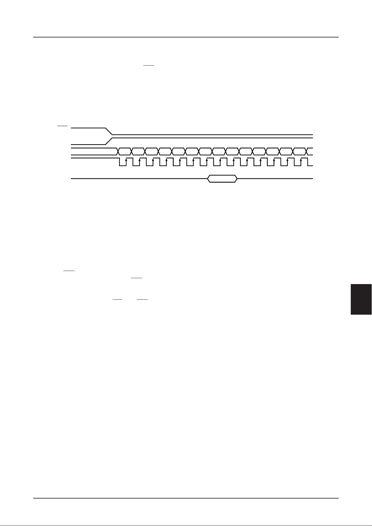
The Serial Interface
When the serial interface has been selected (P/S =
LOW) then when the chip is in active state (CS1 = LOW
and CS2 = HIGH) the serial data input (SI) and the serial
clock input (SCL) can be received. The serial data is
read from the serial data input pin in the rising edge of
the serial clocks D7, D6 through D0, in this order. This
data is converted to 8 bits parallel data in the rising edge
CS1
CS2
SI
SCL
A0
D7
D6 D5 D4 D3 D2 D7 D6 D5 D4 D3 D2D1 D0
1234567891011121314
of the eighth serial clock for the processing.
The A0 input is used to determine whether or the serial
data input is display data or command data; when A0 =
HIGH, the data is display data, and when A0 = LOW
then the data is command data. The A0 input is read and
used for detection every 8th rising edge of the serial
clock after the chip becomes active.
Figure 1 is a serial interface signal chart.
Figure 1
* When the chip is not active, the shift registers and the counter are reset to their initial states.
* Reading is not possible while in serial interface mode.
* Caution is required on the SCL signal when it comes to line-end reflections and external noise. We recommend that
operation be rechecked on the actual equipment.
The Chip Select
The S1D15605 Series chips have two chip select
terminals: CS1 and CS2. The MPU interface or the
serial interface is enabled only when CS1 = LOW and
CS2 = HIGH.
When the chip select is inactive, D0 to D7 enter a high
impedance state, and the A0, RD, and WR inputs are
inactive. When the serial interface is selected, the shift
register and the counter are reset.
Accessing the Display Data RAM and the
Internal Registers
Data transfer at a higher speed is ensured since the MPU
is required to satisfy the cycle time (
tCYC) requirement
alone in accessing the S1D15605 Series. Wait time may
not be considered.
And, in the S1D15605 Series chips, each time data is
sent from the MPU, a type of pipeline process between
LSIs is performed through the bus holder attached to the
internal data bus.
For example, when the MPU writes data to the display
data RAM, once the data is stored in the bus holder, then
it is written to the display data RAM before the next data
write cycle. Moreover, when the MPU reads the display
data RAM, the first data read cycle (dummy) stores the
read data in the bus holder, and then the data is read from
the bus holder to the system bus at the next data read
cycle.
There is a certain restriction in the read sequence of the
display data RAM. Please be advised that data of the
specified address is not generated by the read instruction
issued immediately after the address setup. This data is
generated in data read of the second time. Thus, a
dummy read is required whenever the address setup or
write cycle operation is conducted.
This relationship is shown in Figure 2.
Rev. 2.4a EPSON 8–25
Page 28

S1D15605 Series
The Busy Flag
When the busy flag is “1” it indicates that the S1D15605
Series chip is running internal processes, and at this
time no command aside from a status read will be
received. The busy flag is outputted to D7 pin with the
WR
MPU
DATA
BUS Holder
Write Signal
Internal Timing
WR
RD
MPU
DATA
N
Latch
N
N N n n+1
read instruction. If the cycle time (
it is not necessary to check for this flag before each
command. This makes vast improvements in MPU
processing capabilities possible.
Writing
N+1 N+2 N+3
N+1 N+2 N+3
Reading
tCYC) is maintained,
Address Preset
Read Signal
Column Address
Internal Timing
Bus Holder
Address Set
#n
N+2Increment N+1Preset N
N n n+1 n+2
Dummy
Read
Data Read
#n
Data Read
#n+1
Figure 2
8–26 EPSON Rev. 2.4a
Page 29

S1D15605 Series
Display Data RAM
Display Data RAM
The display data RAM is a RAM that stores the dot data
for the display. It has a 65 (8 page × 8 bit +1) × 132 bit
structure. It is possible to access the desired bit by
specifying the page address and the column address.
Because, as is shown in Figure 3, the D7 to D0 display
data from the MPU corresponds to the liquid crystal
display common direction, there are few constraints at
D0
0
D1
1
D2
0
D3
0
D4
1
—
Display data RAM
1
1
1
0
0
0
0
0
0
1
1
1
0
0
0
0
0
0
0
0
the time of display data transfer when multiple S1D15605
series chips are used, thus and display structures can be
created easily and with a high degree of freedom.
Moreover, reading from and writing to the display
RAM from the MPU side is performed through the I/O
buffer, which is an independent operation from signal
reading for the liquid crystal driver. Consequently, even
if the display data RAM is accessed asynchronously
during liquid crystal display, it will not cause adverse
effects on the display (such as flickering).
COM0
COM1
COM2
COM3
COM4
—
Liquid crystal display
Figure 3
The Page Address Circuit
As shown in Figure 6-4, page address of the display data
RAM is specified through the Page Address Set
Command. The page address must be specified again
when changing pages to perform access.
Page address 8 (D3, D2, D1, D0 = 1, 0, 0, 0) is the page
for the RAM region used only by the indicators, and
only display data D0 is used.
The Column Addresses
As is shown in Figure 4, the display data RAM column
address is specified by the Column Address Set
command. The specified column address is incremented
(+1) with each display data read/write command. This
allows the MPU display data to be accessed continuously.
Moreover, the incrementation of column addresses stops
with 83H. Because the column address is independent
of the page address, when moving, for example, from
page 0 column 83H to page 1 column 00H, it is necessary
to respecify both the page address and the column
address.
Furthermore, as is shown in Table 4, the ADC command
(segment driver direction select command) can be used
to reverse the relationship between the display data
RAM column address and the segment output. Because
of this, the constraints on the IC layout when the LCD
module is assembled can be minimized.
Table 4
SEG
Output
SEG0 SEG 131
ADC “0” 0 (H) → Column Address → 83 (H)
(D0) “1” 83 (H) ← Column Address ← 0 (H)
The Line Address Circuit
The line address circuit, as shown in Table 4, specifies
the line address relating to the COM output when the
contents of the display data RAM are displayed. Using
the display start line address set command, what is
normally the top line of the display can be specified (this
is the COM0 output when the common output mode is
normal, and the COM63 output for S1D15605 Series,
COM47 output for S1D15606 Series, COM31 output for
the S1D15607 Series, COM53 output for S1D15608
and COM51 output for S1D15609
output mode is reversed. The display area is a 65 line area
*****
) when the common
*****
for the S1D15605 Series, a 49 line are for the S1D15606,
a 33 line area for the S1D15607 Series , 55 line area for
the S1D15608
S1D15609
If the line addresses are changed dynamically using the
*****
*****
and 53 line area for the
from the display start line address.
display start line address set command, screen scrolling,
page swapping, etc. can be performed.
Rev. 2.4a EPSON 8–27
Page 30

S1D15605 Series
Page Address
D3 D2 D1 D0
Data
D0
D1
D2
0 0 0 0 Page 0
D3
D4
D5
D6
D7
D0
D1
D2
0 0 0 1 Page 1
D3
D4
D5
D6
D7
D0
D1
D2
0 0 1 0 Page 2
D3
D4
D5
D6
D7
D0
D1
D2
0 0 1 1 Page 3
D3
D4
D5
D6
D7
D0
D1
D2
0 1 0 0 Page 4
D3
D4
D5
D6
D7
D0
D1
D2
0 1 0 1 Page 5
D3
D4
D5
D6
D7
D0
D1
D2
0 1 1 0 Page 6
D3
D4
D5
D6
D7
D0
D1
D2
0 1 1 1 Page 7
D3
D4
D5
D6
1000
D7
D0
Page 8
Line
Address
00H
01H
02H
03H
04H
05H
06H
07H
08H
09H
0AH
0BH
0CH
0DH
0EH
0FH
11H
12H
13H
14H
15H
16H
17H
18H
18H
19H
1AH
1BH
1CH
1DH
1EH
1FH
20H
21H
22H
23H
24H
25H
26H
27H
28H
29H
2AH
2BH
2CH
2DH
2EH
2FH
30H
31H
32H
33H
34H
35H
36H
37H
38H
39H
3AH
3BH
3CH
3DH
3EH
3FH
When the
common output
mode is normal
48 lines
52 lines
54 lines
63 lines
Start
32 lines
COM
Output
COM0
COM1
COM2
COM3
COM4
COM5
COM6
COM7
COM8
COM9
COM10
COM11
COM12
COM13
COM14
COM15
COM16
COM17
COM18
COM19
COM20
COM21
COM22
COM23
COM24
COM25
COM26
COM27
COM28
COM29
COM30
COM31
COM32
COM33
COM34
COM35
COM36
COM37
COM38
COM39
COM40
COM41
COM42
COM43
COM44
COM45
COM46
COM47
COM48
COM49
COM50
COM51
COM52
COM53
COM54
COM55
COM56
COM57
COM58
COM59
COM60
COM61
COM62
COM63
COMS
00010203040506
838281
SEG0
SEG1
SEG2
80
7F
SEG3
SEG4
7E
7D
SEG5
SEG6
07
7C
SEG7
808182
7F
7E
7C
7D
07060504030201
SEG127
SEG125
SEG126
SEG127
SEG128
SEG129
SEG130
0
83
1
00
SEG131
D0
D0
LCD
ADC
Out
Regardless of the display
start line address, the
S1D15605 Series
Column
accesses 65th line, the
Address
S1D15606 Series
accesses 49th line and
the S1D15607 Series
accesses 33th line and
the S1D15608 Series
accesses 55th line, the
S1D15609 Series
accesses 53 lines.
Figure 4
8–28 EPSON Rev. 2.4a
Page 31

S1D15605 Series
The Display Data Latch Circuit
The display data latch circuit is a latch that temporarily
stores the display data that is output to the liquid crystal
driver circuit from the display data RAM.
Because the display normal/reverse status, display ON/
OFF status, and display all points ON/OFF commands
control only the data within the latch, they do not change
the data within the display data RAM itself.
Display Timing Generator Circuit
The display timing generator circuit generates the timing
signal to the line address circuit and the display data
latch circuit using the display clock. The display data is
latched into the display data latch circuit synchronized
with the display clock, and is output to the data driver
output terminal. Reading to the display data liquid
crystal driver circuits is completely independent of
accesses to the display data RAM by the MPU.
The Oscillator Circuit
This is a CR-type oscillator that produces the display
clock. The oscillator circuit is only enabled when M/S
= HIGH and CLS = HIGH.
When CLS = LOW the oscillation stops, and the display
clock is input through the CL terminal.
Consequently, even if the display data RAM is accessed
asynchronously during liquid crystal display, there is
absolutely no adverse effect (such as flickering) on the
display.
Moreover, the display timing generator circuit generates
the common timing and the liquid crystal alternating
current signal (FR) from the display clock. It generates
a drive wave form using a 2 frame alternating current
drive method, as is shown in Figure 5, for the liquid
crystal drive circuit.
Two-frame alternating current drive wave form (S1D15605
65 1 2 3 4 5 6 60 61 62 63 64 65 1 2 3 4 5 6
64
CL
*****
)
FR
COM0
COM1
RAM
DATA
SEGn
Figure 5
DD
V
V
1
V
4
V
5
V
DD
V
1
V
4
V
5
V
DD
V
2
V
3
V
5
Rev. 2.4a EPSON 8–29
Page 32

S1D15605 Series
When multiple S1D15605 Series chips are used, the
slave chips must be supplied the display timing signals
(FR, CL, DOF) from the master chip[s].
Table 5 shows the status of the FR, CL, and DOF
signals.
Table 5
Operating Mode FR CL DOF
Master (M/S = HIGH)The internal oscillator circuit is enabled (CLS = HIGH) Output Output Output
The internal oscillator circuit is disabled (CLS = LOW) Output Input Output
Slave (M/S = LOW) Set the CLS pin to the same level as with the master. Input Input Input
Input Input Input
The Common Output Status Select
Circuit
In the S1D15605 Series chips, the COM output scan
direction can be selected by the common output status
select command. (See Table 6.) Consequently, the
constraints in IC layout at the time of LCD module
assembly can be minimized.
Table 6
Status COM Scan Direction
S1D15605
Normal COM0 → COM63 COM0 → COM47 COM0 → COM31 COM0 → COM53 COM0 → COM51
Reverse COM63 → COM0 COM47 → COM0 COM31 → COM0 COM53 → COM0 COM51 → COM0
*****
S1D15606
*****
S1D15607
*****
S1D15608
*****
S1D15609
*****
The Liquid Crystal Driver Circuits
These are a 197-channel (S1D15605 Series), a 181channel (S1D15606 Series) multiplexers 165-channel
(S1D15607 Series), 187-channel (S1D15608 Series)
and a 185-channel (S1D15609 Series) that generate
four voltage levels for driving the liquid crystal. The
combination of the display data, the COM scan signal,
and the FR signal produces the liquid crystal drive
voltage output.
Figure 6 shows examples of the SEG and COM output
wave form.
8–30 EPSON Rev. 2.4a
Page 33

S1D15605 Series
COM0
COM1
COM2
COM3
COM4
COM5
COM6
COM7
COM8
COM9
COM10
COM11
COM12
COM13
COM14
COM15
FR
COM0
COM1
COM2
SEG0
SEG1
SEG2
V
DD
V
SS
V
DD
V
1
V
2
V
3
V
4
V
5
V
DD
V
1
V
2
V
3
V
4
V
5
V
DD
V
1
V
2
V
3
V
4
V
5
V
DD
V
1
V
2
V
3
V
4
V
5
V
DD
V
1
V
2
V
3
V
4
V
5
V
DD
V
1
V
2
V
3
V
4
V
5
COM0–SEG0
COM0–SEG1
Figure 6
V
V
V
V
V
V
–V
–V
–V
–V
–V
V
V
V
V
V
V
–V
–V
–V
–V
–V
5
4
3
2
1
∞
1
2
3
4
5
5
4
3
2
1
∞
1
2
3
4
5
Rev. 2.4a EPSON 8–31
Page 34

S1D15605 Series
operation.
The Power Supply Circuits
The power supply circuits are low-power consumption
power supply circuits that generate the voltage levels
required for the liquid crystal drivers. They comprise
Booster circuits, voltage regulator circuits, and voltage
follower circuits. They are only enabled in master
Table 7 The Control Details of Each Bit of the Power Control Set Command
Item
D2 Booster circuit control bit ON OFF
D1 Voltage regulator circuit (V regulator circuit) control bit ON OFF
D0 Voltage follower circuit (V/F circuit) control bit ON OFF
Table 8 Reference Combinations
Use Settings D2 D1 D0
1
Only the internal power supply is 1 1 1 O O O VSS2 Used
used
2
Only the V regulator circuit and 0 1 1 X O O VOUT, VSS2 Open
the V/F circuit are used
3
Only the V/F circuit is used 0 0 1 X X O V5, VSS2 Open
4
Only the external power supply is 0 0 0 X X X V1 to V5 Open
used
* The “step-up system terminals” refer CAP1+, CAP1–, CAP2+, CAP2–, and CAP3–.
* While other combinations, not shown above, are also possible, these combinations are not recommended
because they have no practical use.
The power supply circuits can turn the Booster circuits,
the voltage regulator circuits, and the voltage follower
circuits ON of OFF independently through the use of the
Power Control Set command. Consequently, it is possible
to make an external power supply and the internal
power supply function somewhat in parallel. Table 7
shows the Power Control Set Command 3-bit data
control function, and Table 8 shows reference
combinations.
Status
“1” “0”
Step-up
voltage
system
terminal
Step-up
circuit
V External
regulator
circuit
V/F
circuit
voltage
input
The Step-up Voltage Circuits
Using the step-up voltage circuits equipped within the
S1D15605 Series chips it is possible to product a Quad
step-up, a Triple step-up, and a Double step-up of the
V
DD – VSS2 voltage levels.
Quad step-up: Connect capacitor C1 between CAP1+
and CAP1–, between CAP2+ and CAP2–,
between CAP1+ and CAP3–, and between
V
SS2 and VOUT, to produce a voltage level
in the negative direction at the V
OUT
terminal that is 4 times the voltage level
between V
DD and VSS2.
Triple step-up: Connect capacitor C1 between CAP1+
and CAP1–, between CAP2+ and CAP2–
and between V
between CAP3– and V
SS2 and VOUT, and short
OUT to produce a
voltage level in the negative direction at the
V
OUT terminal that is 3 times the voltage
difference between V
DD and VSS2.
Double step-up: Connect capacitor C1 between
CAP1+ and CAP1–, and between V
V
OUT, leave CAP2+ open, and short
between CAP2–, CAP3– and V
SS2 and
OUT to
produce a voltage in the negative direction
at the V
OUT terminal that is twice the voltage
between V
DD and VSS2.
The step-up voltage relationships are shown in Figure 7.
8–32 EPSON Rev. 2.4a
Page 35

C1
S1D15605 Series
V
V
SS2
OUT
+
C1
+
V
SS2
V
OUT
+
C1
V
V
SS2
OUT
C1
+
C1
C1
+
4 x step-up voltage circuit 3 x step-up voltage circuit 2 x step-up voltage circuit
VDD = 0V
V
SS2 = –3V
V
OUT = 4 x VSS2 = –12V
4x step-up voltage relationships
CAP3–
CAP1+
CAP1–
CAP2–
CAP2+
S1D15605 Series
V
V
V
OUT = 3 x VSS2 = –9V
+
C1
C1
+
DD = 0V
SS2 = –3V
3x step-up voltage relationships
CAP3–
CAP1+
CAP1–
CAP2–
CAP2+
S1D15605 Series
DD = 0V
V
V
SS2 = –5V
V
OUT = 2 x VSS2 = –10V
2x step-up voltage relationships
C1
CAP3–
+
CAP1+
CAP1–
CAP2–
CAP2+OPEN
S1D15605 Series
* The V
SS2 voltage range must be set so that the VOUT terminal voltage does not exceed the absolute maximum rated
value.
The Voltage Regulator Circuit
The step-up voltage generated at V
liquid crystal driver voltage V
OUT outputs the
5 through the voltage
regulator circuit.
Because the S1D15605 Series chips have an internal
high-accuracy fixed voltage power supply with a 64level electronic volume function and internal resistors
for the V
5 voltage regulator, systems can be constructed
without having to include high-accuracy voltage
regulator circuit components.
Moreover, in the S1D15605 Series, three types of thermal
gradients have been prepared as V
REG options: (1)
approximately -0.05%/°C (2) approximately -0.2%/°C,
and (3) external input (supplied to the V
RS terminal).
Figure 7
(A) When the V5 Voltage Regulator Internal
Resistors Are Used
Through the use of the V
5 voltage regulator internal
resistors and the electronic volume function the liquid
crystal power supply voltage V
5 can be controlled by
commands alone (without adding any external resistors),
making it possible to adjust the liquid crystal display
brightness. The V
equation A-1 over the range where | V
5 voltage can be calculated using
5 | < | VOUT |.
Rev. 2.4a EPSON 8–33
Page 36

S1D15605 Series
Rb
V
=+
5
=+
Q
[]
1
11
∴
VV
⋅
V
EV
Ra
Rb
Ra
=−
()
EV REG
α
⋅
1
–
⋅
V
REG
162
α
⋅
162
VEV (constant voltage supply + electronic volume)
(Equation A-1)
V
DD
Internal Ra
Internal Rb
V
REG is the IC-internal fixed voltage supply, and its
voltage at Ta = 25°C is as shown in Table 9.
Equipment Type Thermal Gradient Units VREG Units
(1) Internal Power Supply –0.05 [%/°C ] –2.1 [V]
(2) Internal Power Supply –0.2 [%/°C ] –4.9 [V]
(3) External Input — — V
+
–
Figure 8
Table 9
V
5
RS [V]
α is set to 1 level of 64 possible levels by the electronic
volume function depending on the data set in the 6-bit
electronic volume register. Table 10 shows the value for
α depending on the electronic volume register settings.
Table 10
D5 D4 D3 D2 D1 D0 α
Rb/Ra is the V
5 voltage regulator internal resistor ratio,
and can be set to 8 different levels through the V
voltage regulator internal resistor ratio set command.
The (1 + Rb/Ra) ratio assumes the values shown in
Table 11 depending on the 3-bit data settings in the V
voltage regulator internal resistor ratio register.
00000063
00000162
00001061
..
..
..
111101 2
111110 1
111111 0
8–34 EPSON Rev. 2.4a
5
5
Page 37

S1D15605 Series
V5 voltage regulator internal resistance ratio register
value and (1 + Rb/Ra) ratio (Reference value)
Table 11
S1D15605
Register Equipment Type by Thermal Gradient [Units: %/
D2 D1 D0 (1) –0.05 (2) –0.2 (3) VREG External Input (1) –0.05 (2) –0.2 (3) VREG External Input
0 0 0 3.0 1.3 1.5 3.0 1.3 1.5
0 0 1 3.5 1.5 2.0 3.5 1.5 2.0
0 1 0 4.0 1.8 2.5 4.0 1.8 2.5
0 1 1 4.5 2.0 3.0 4.5 2.0 3.0
1 0 0 5.0 2.3 3.5 5.0 2.3 3.5
1 0 1 5.5 2.5 4.0 5.4 2.5 4.0
1 1 0 6.0 2.8 4.5 5.9 2.8 4.5
1 1 1 6.4 3.0 5.0 6.4 3.0 5.0
*****
°
C ] Equipment Type by Thermal Gradient [Units: %/
S1D15606
*****
°
C ]
S1D15607
Register Equipment Type by Thermal Gradient [Units: %/
D2 D1 D0 (1) –0.05 (2) –0.2 (3) VREG External Input –0.05
0 0 0 3.0 1.3 1.5 3
0 0 1 3.5 1.5 2.0 3.5
0 1 0 4.0 1.8 2.5 4
0 1 1 4.5 2.0 3.0 4.5
1 0 0 5.0 2.3 3.5 5
1 0 1 5.4 2.5 4.0 5.4
1 1 0 5.9 2.8 4.5 5.9
1 1 1 6.4 3.0 5.0 6.4
For the internal resistance ratio, a manufacturing
dispersion of up to ±7% should be taken into account.
When not within the tolerance, adjust the V
externally mounting Ra and Rb.
Figs. 9, 10, 11 (for S1D15605 Series), 12, 13, 14 (for
S1D15606 Series), 15, 16, 17 (for S1D15607 Series), 18
(for S1D15608D00B
S1D15609D00B
of the internal resistance ratio resistor for V
adjustment and electric volume resister for each
temperature grade model, when Ta = 25 °C.
) show V5 voltage measured by values
*
) and Figs. 19 (for
*
*****
5 voltage by
5 voltage
°
C ] Equipment Type by Thermal Gradient [Units: %/
S1D15608
*****
/S1D15609
*****
°
C ]
Rev. 2.4a EPSON 8–35
Page 38

S1D15605 Series
–16
–15
–14
–13
–12
–11
–10
V5 [v]
–9
–8
–7
–6
–5
–4
–3
–2
–1
S1D15605D00B*/S1D15605D11B
0
00H
18H
*
30H
Electric Volume
Resister
1 1 1
1 1 0
1 0 1
1 0 0
0 1 1
0 1 0
0 0 1
0 0 0
5
voltage
The V
regulator internal
resistance ratio
registers
(D2, D1, D0)
3FH
Figure 9: S1D15605D00B*/S1D15605D11B* (1) For Models Where the Thermal Gradient = -0.05%/°C
The V
5 voltage as a function of the V5 voltage regulator internal resistor ratio register and the electronic
volume register.
–16
–15
–14
–13
–12
–11
–10
V5 [v]
–9
–8
–7
–6
–5
–4
–3
–2
–1
S1D15605D01B
0
00H
18H
*
The V5 voltage
regulator internal
resistance ratio
registers
(D2, D1, D0)
Electric Volume
30H
Resister
3FH
Figure 10: S1D15605D01B* (2) For Models Where the Thermal Gradient = -0.2%/°C
1 1 1
1 1 0
1 0 1
1 0 0
0 1 1
0 1 0
0 0 1
0 0 0
The V
5 voltage as a function of the V5 voltage regulator internal resistor ratio register and the electronic
volume register.
8–36 EPSON Rev. 2.4a
Page 39

S1D15605 Series
–16
–15
–14
–13
–12
–11
–10
V5 [v]
–9
–8
–7
–6
–5
–4
–3
–2
–1
S1D15605D02B
0
00H
18H
*
The V5 voltage
regulator internal
resistance ratio
registers
(D2, D1, D0)
Electric Volume
30H
Resister
3FH
1 1 1
1 1 0
1 0 1
1 0 0
0 1 1
0 1 0
0 0 1
0 0 0
Figure 11: S1D15605D02B* (3) For models with External Input
The V
5 voltage as a function of the V5 voltage regulator internal resistor ratio register and the electronic
volume register.
–16
–15
–14
–13
–12
–11
–10
V5 [v]
–9
–8
–7
–6
–5
–4
–3
–2
–1
S1D15606D00B
0
00H
18H
/S1D15606D11B
*
*
30H
Electric Volume
Resister
The V5 voltage
regulator internal
resistance ratio
registers
(D2, D1, D0)
3FH
Figure 12: S1D15606D00B*/S1D15606D11B* (1) For Models Where the Thermal Gradient = -0.05%/°C
1 1 1
1 1 0
1 0 1
1 0 0
0 1 1
0 1 0
0 0 1
0 0 0
The V
5 voltage as a function of the V5 voltage regulator internal resistor ratio register and the electronic
volume register.
Rev. 2.4a EPSON 8–37
Page 40

S1D15605 Series
–16
–15
–14
–13
–12
–11
–10
V5 [v]
–9
–8
–7
–6
–5
–4
–3
–2
–1
S1D15606D01B
0
00H
18H
*
The V5 voltage
regulator internal
resistance ratio
registers
(D2, D1, D0)
Electric Volume
30H
Resister
3FH
1 1 1
1 1 0
1 0 1
1 0 0
0 1 1
0 1 0
0 0 1
0 0 0
Figure 13: S1D15606D01B* (2) For Models Where the Thermal Gradient = -0.2%/°C
The V
5 voltage as a function of the V5 voltage regulator internal resistor ratio register and the electronic
volume register.
–16
–15
–14
–13
–12
–11
–10
V5 [v]
–9
–8
–7
–6
–5
–4
–3
–2
–1
S1D15606D
0
00H
18H
02B
*
The V5 voltage
regulator internal
resistance ratio
registers
(D2, D1, D0)
Electric Volume
30H
Resister
3FH
1 1 1
1 1 0
1 0 1
1 0 0
0 1 1
0 1 0
0 0 1
0 0 0
Figure 14: S1D15606D02B
The V
5 voltage as a function of the V5 voltage regulator internal resistor ratio register and the electronic
(3) For models with External Input
*
volume register.
8–38 EPSON Rev. 2.4a
Page 41

S1D15605 Series
–16
–15
–14
–13
–12
–11
–10
V5 [v]
–9
–8
–7
–6
–5
–4
–3
–2
–1
S1D15607D00B*/S1D15607D11B
0
00H
18H
*
Electric Volume
30H
Resister
1 1 1
1 1 0
1 0 1
1 0 0
0 1 1
0 1 0
0 0 1
0 0 0
The V5 voltage
regulator internal
resistance ratio
registers
(D2, D1, D0)
3FH
Figure 15: S1D15607D00B*/S1D15607D11B* (1) For Models Where the Thermal Gradient = -0.05%/°C
The V
5 voltage as a function of the V5 voltage regulator internal resistor ratio register and the electronic
volume register.
–16
–15
–14
–13
–12
–11
–10
V5 [v]
–9
–8
–7
–6
–5
–4
–3
–2
–1
0
00H
S1D15607D01B
18H
*
The V5 voltage
regulator internal
resistance ratio
registers
(D2, D1, D0)
Electric Volume
30H
Resister
3FH
1 1 1
1 1 0
1 0 1
1 0 0
0 1 1
0 1 0
0 0 1
0 0 0
Figure 16: S1D15607D01B* (2) For Models Where the Thermal Gradient = -0.2%/°C
The V
5 voltage as a function of the V5 voltage regulator internal resistor ratio register and the electronic
volume register.
Rev. 2.4a EPSON 8–39
Page 42

S1D15605 Series
–16
–15
–14
–13
–12
–11
–10
V5 [v]
–9
–8
–7
–6
–5
–4
–3
–2
–1
S1D15607D02B
0
00H
18H
*
The V5 voltage
regulator internal
resistance ratio
registers
(D2, D1, D0)
Electric Volume
30H
Resister
3FH
1 1 1
1 1 0
1 0 1
1 0 0
0 1 1
0 1 0
0 0 1
0 0 0
Figure 17: S1D15607D02B* (3) For models with External Input
The V
5 voltage as a function of the V5 voltage regulator internal resistor ratio register and the electronic
volume register.
–16
–15
–14
–13
–12
–11
–10
V5 [v]
–9
–8
–7
–6
–5
–4
–3
–2
–1
0
00H
S1D15608D00B
18H
*
The V
regulator internal
resistance ratio
registers
(D2, D1, D0)
Electric Volume
30H
Resister
3FH
5
voltage
1 1 1
1 1 0
1 0 1
1 0 0
0 1 1
0 1 0
0 0 1
0 0 0
Figure 18: S1D15608D00B* (1) For Models Where the Thermal Gradient = –0.05%/°C
The V
5 voltage as a function of the V5 voltage regulator internal resistor ratio register and the electronic
volume register.
8–40 EPSON Rev. 2.4a
Page 43

S1D15605 Series
–16
–15
–14
–13
–12
–11
–10
–9
–8
V5 [v]
–7
–6
–5
–4
–3
–2
–1
S1D15609D00B
0
00H
18H
*
1 1 1
1 1 0
1 0 1
1 0 0
0 1 1
0 1 0
0 0 1
0 0 0
The V5 voltage
regulator internal
resistance ratio
registers
(D2, D1, D0)
Electric Volume
30H
Resister
3FH
Figure 19: S1D15609D00B* Temperature Gradient = –0.05%/°C Model
The V
5 voltage as a function of the V5 voltage regulator internal resistor ratio register and the electronic
volume register.
Setup example: When selecting Ta = 25°C and V5 = 7
V for an S1D15607 model on which Temperature
gradient = –0.05%/°C.
At this time, the variable range and the notch width of
the V
5 voltage is, as shown Table 13, as dependent on
the electronic volume.
Using Figure 15 and the equation A-1, the following
setup is enabled.
Table 12
Contents
5 voltage — — — 0 1 0
For V
D5 D4 D3 D2 D1 D0
Register
regulator
Electronic Volume 1 0 0 1 0 1
Table 13
V5 Min. Typ. Max. Units
Variable Range –8.4 (63 levels) –6.8 (central value) –5.1 (0 level) [V]
Notch width 51 [mV]
Rev. 2.4a EPSON 8–41
Page 44

S1D15605 Series
(B) When an External Resistance is Used
(i.e., The V5 Voltage Regulator Internal
Resistors Are Not Used) (1)
The liquid crystal power supply voltage V
set without using the V
5 voltage regulator internal
5 can also be
resistors (IRS terminal = LOW) by adding resistors Ra’
and Rb’ between V
DD and VR, and between VR and V5,
'
Rb
V
=+
5
=+
Q
[]
External
resistor Ra'
1
11
∴
VV
EV REG
V
⋅
EV
'
Ra
'
Rb
'
Ra
1
=−
()
α
⋅
α
–
162
162
V
⋅
REG
⋅
VEV (fixed voltage power supply + electronic volume)
+
–
respectively. When this is done, the use of the electronic
volume function makes it possible to adjust the brightness
of the liquid crystal display by controlling the liquid
crystal power supply voltage V
In the range where | V
be calculated using equation B-1 based on the external
resistances Ra’ and Rb’.
( Equation B-1)
5 through commands.
5 | < | VOUT |, the V5 voltage can
V
DD
V
5
External
resistor Rb'
Setup example: When selecting Ta = 25°C and V
5 = –
7 V for an S1D15607 Series model where the temperature
gradient = –0.05%/°C.
When the central value of the electron volume register
is (D5, D4, D3, D2, D1, D0) = (1, 0, 0, 0, 0, 0), then α
= 31 and V
REG = –2.1 V so, according to equation B-1,
'
Rb
V
11
=+
'
Ra
'
Rb
11 1 1
−=+
V
'
Ra
⋅−
⋅−
α
162
31
162
⋅
V
REG5
.
21
⋅−
()
(Equation B-2)
Moreover, when the value of the current running through
Ra’ and Rb’ is set to 5 µA,
Ra Rb M''.+=14 Ω
(Equation B-3)
V5 Min. Typ. Max. Units
Variable Range –8.6 (63 levels) –7.0 (central value) –5.3 (0 level) [V]
Notch width 52 [mV]
Figure 20
Table 14
Consequently, by equations B-2 and B-3,
Rb
'
.
=
312
Ra
'
Ra k
'
=Ω
340
Rb k
'
=Ω
1060
At this time, the V5 voltage variable range and notch
width, based on the electron volume function, is as
given in Table 14.
8–42 EPSON Rev. 2.4a
Page 45

S1D15605 Series
Rk
Rk
Rk
1
2
3
264
211
925
=Ω
=Ω
=Ω
(C) When External Resistors are Used
(i.e. The V
5 Voltage Regulator Internal
Resistors Are Not Used). (2)
When the external resistor described above are used,
adding a variable resistor as well makes it possible to
perform fine adjustments on Ra’ and Rb’, to set the
liquid crystal drive voltage V
V
=+
5
=+
Q
[]
Ra'
5. In this case, the use of
RR R
+−
32 2
1
RR
11
∴
VV
EV REG
+∆
12
RR R
+−∆
32 2
RR
+∆
12
α
1
=−
()
External
resistor R
External
resistor R
162
∆
V
⋅
EV
α
⋅
⋅
1
2
–
∆R
V
R
162
2
V
⋅
the electronic volume function makes it possible to
control the liquid crystal power supply voltage V
commands to adjust the liquid crystal display brightness.
In the range where | V
5 | < | VOUT | the V5 voltage can
be calculated by equation C-1 below based on the R
and R2 (variable resistor) and R3 settings, where R2 can
be subjected to fine adjustments (∆ R
REG
(Equation C-1)
V
DD
VEV (fixed voltage supply + electronic volume)
+
V
5
–
5 by
1
2).
Rb'
Setup example: When selecting Ta = 25°C and V
External
resistor R
3
5 = –
5 to –9 V (using R2) for an S1D15607 model where the
temperature gradient = –0.05%/°C.
When the central value for the electronic volume register
is set at (D5, D4, D3, D2, D1, D0) = (1, 0, 0, 0, 0, 0),
α
==−31
.
REG
21VV
so, according to equation C-1, when ∆ R2 = 0 Ω, in order
to make V
5 = –9 V,
RR
−=+
91 1
V
+
32
⋅−
R
1
31
162
⋅−
21
.
()
(Equation C-2)
Figure 21
When ∆ R
2 = R2, in order to make V = –5 V,
−=+
51 1
V
R
3
+
RR
12
⋅−
162
31
⋅−
21
.
()
(Equation C-3)
Moreover, when the current flowing V
DD and V5 is set
to 5 µA,
RRR M
123
14++= Ω.
(Equation C-4)
With this, according to equation C-2, C-3 and C-4,
At this time, the V5 voltage variable range and notch
width based on the electron volume function is as shown
in Table 15.
Rev. 2.4a EPSON 8–43
Table 15
V5 Min. Typ. Max. Units
Variable Range –8.7 (63 levels) –7.0 (central value) –5.3 (0 level) [V]
Notch width 53 [mV]
Page 46

S1D15605 Series
* When the V5 voltage regulator internal resistors or
the electronic volume function is used, it is necessary
to at least set the voltage regulator circuit and the
voltage follower circuit to an operating mode using
the power control set commands. Moreover, it is
necessary to provide a voltage from V
OUT when the
Booster circuit is OFF.
* The V
R terminal is enabled only when the V5 voltage
regulator internal resistors are not uesd (i.e. the IRS
terminal = LOW). When the V
5 voltage regulator
internal resistors are uesd (i.e. when the IRS terminal
= HIGH), then the V
* Because the input impedance of the V
R terminal is left open.
R terminal is
high, it is necessary to take into consideration short
leads, shield cables, etc. to handle noise.
The Liquid Crystal Voltage Generator Circuit
5 voltage is produced by a resistive voltage
The V
divider within the IC, and can be produced at the V
V
3, and V4 voltage levels required for liquid crystal
1, V2,
driving. Moreover, when the voltage follower changes
the impedance, it provides V
1, V2, V3 and V4 to the
liquid crystal drive circuit. 1/9 bias or 1/7 bias for
S1D15605 Series, 1/8 bias or 1/6 bias for S1D15606
Series, 1/6 bias or 1/5 bias for the S1D15607 Series, 1/
8 bias or 1/6 bias for S1D15608 Series and 1/8 bias or
1/6 bias for S1D15609 Series can be selected.
High Power Mode
The power supply circuit equipped in the S1D15605
Series chips has very low power consumption (normal
mode: HPM = HIGH). However, for LCDs or panels
with large loads, this low-power power supply may
cause display quality to degrade. When this occurs,
setting the HPM terminal to LOW (high power mode)
can improve the quality of the display. We recommend
that the display be checked on actual equipment to
determine whether or not to use this mode.
Moreover, if the improvement to the display is inadequate
even after high power mode has been set, then it is
necessary to add a liquid crystal drive power supply
externally.
The Internal Power Supply Shutdown
Command Sequence
The sequence shown in Figure 22 is recommended for
shutting down the internal power supply, first placing
the power supply in power saver mode and then turning
the power supply OFF.
Sequence
Step1
Step2
End
Details
(Command, status)
Display OFF
Display all points ON
Internal power supply OFF
Command address
D7
D6
D5
1
0
1
1
0
1
Figure 22
D4
0
0
D3
1
0
D2
1
1
D1
1
0
D0
0
1
Power saver
commands
(compound)
8–44 EPSON Rev. 2.4a
Page 47

Reference Circuit Examples
Figure 22 shows reference circuit examples.
➀ When used all of the step-up circuit, voltage regulating circuit and V/F circuit
(1) When the voltage regulator internal resistor
is used.
SS2
(Example where V
V
DD
= VSS, with 4x step-up)
(2) When the voltage regulator internal resistor
is not used.
(Example where V
S1D15605 Series
SS2
= VSS, with 4x step-up)
V
DD
IRS M/S
V
SS2
C
1
V
V
SS
V
DD
C
2
C
2
C
2
C
2
C
2
OUT
CAP3–
C
1
CAP1+
1
C
CAP1–
CAP2+
C
1
CAP2–
5
V
V
R
V
DD
V
1
V
2
V
3
V
4
V
5
S1D15605 Series
➁ When the voltage regulator circuit and V/F
circuit alone are used
5
(1) When the V
voltage regulator internal resistor
is not used.
V
SS
R
R
V
DD
R
(2) When the V
is used.
IRS M/S
V
SS2
C
1
V
OUT
CAP3–
C
1
CAP1+
1
C
CAP1–
CAP2+
C
1
3
2
1
C
2
C
2
C
2
C
2
C
2
5
voltage regulator internal resistor
CAP2–
5
V
V
R
V
DD
V
1
V
2
V
3
V
4
V
5
S1D15605 Series
V
V
V
DD
SS
DD
External
power
supply
C
C
C
C
C
IRS M/S
V
SS2
V
OUT
CAP3–
CAP1+
CAP1–
CAP2+
CAP2–
5
V
V
R
V
DD
2
2
2
2
2
V
1
V
2
V
3
V
4
V
5
S1D15605 Series
V
DD
IRS M/S
V
SS2
V
V
SS
External
power
supply
OUT
CAP3–
CAP1+
CAP1–
CAP2+
CAP2–
3
R
R
2
V
DD
R
1
C
2
C
2
C
2
C
2
C
2
5
V
V
R
V
DD
V
1
V
2
V
3
V
4
V
5
S1D15605 Series
Rev. 2.4a EPSON 8–45
Page 48

S1D15605 Series
➂ When the V/F circuit alone is used
V
DD
IRS M/S
SS2
V
V
V
SS
External
power
supply
OUT
CAP3–
CAP1+
CAP1–
CAP2+
CAP2–
V
5
V
V
DD
C
2
C
2
C
2
C
2
C
2
R
V
DD
V
1
V
2
V
3
V
4
V
5
S1D15605 Series
5 When the built-in power circuit is used to drive a
liquid crystal panel heavily loaded with AC or DC, it
is recommended to connect an external resistor to
stabilize potentials of V
1, V2, V3 and V4 which are
output from the built-in voltage follower.
➃ When the built-in power is not used
SS
V
V
IRS M/S
V
SS2
V
OUT
CAP3–
CAP1+
CAP1–
CAP2+
CAP2–
V
5
V
V
DD
External
power
supply
R
V
DD
V
1
V
2
V
3
V
4
V
5
S1D15605 Series
Examples of shared reference settings
When V5 can vary between –8 and 12 V
Item Set value Units
1 1.0 to 4.7 µF
C
C2 0.01 to 1.0 µF
DD
VDD, V
0
R
4
C
2
R
4
V
1
V
2
V
3
S1D15605 Series
V
4
Reference set value R4: 100kΩ ~ 1MΩ
R
4
R
4
It is recommended to set an optimum
resistance value R4 taking the liquid crystal
display and the drive waveform.
V
5
Figure 23
* 1 Because the V
R terminal input impedance is high, use short leads and shielded lines.
* 2 C1 and C2 are determined by the size of the LCD being driven. Select a value that will stabilize the liquid crystal
drive voltage.
Example of the Process by which to Determine the Settings:
• Turn the voltage regulator circuit and voltage follower circuit ON and supply a voltage to V
OUT from the outside.
• Determine C2 by displaying an LCD pattern with a heavy load (such as horizontal stripes) and selecting a C2 that
stabilizes the liquid crystal drive voltages (V
1 to V5). Note that all C2 capacitors must have the same capacitance
value.
• Next turn all the power supplies ON and determine C1.
8–46 EPSON Rev. 2.4a
Page 49

S1D15605 Series
* Precautions when installing the COG
When installing the COG, it is necessary to duly consider
the fact that there exists a resistance of the ITO wiring
occurring between the driver chip and the externally
connected parts (such as capacitors and resistors). By the
influence of this resistance, non-conformity may occur
with the indications on the liquid crystal display.
Therefore, when installing the COG design the module
paying sufficient considerations to the following three
points.
1. Suppress the resistance occurring between the driver
chip pin to the externally connected parts as much as
possible.
2. Suppress the resistance connecting to the power
supply pin of the driver chip.
3. Make various COG module samples with different
ITO sheet resistance to select the module with the
sheet resistance with sufficient operation margin.
Also, as for this driver IC, pay sufficient attention to the
following points when connecting to external parts for
the characteristics of the circuit.
1. Connection to the boosting capacitors The boosting
capacitors (the capacitors connecting to respective
CAP pins and capacitor being inserted between
V
OUT and VSS2) of this IC are being switched over
by use of the transistor with very low ON-resistance
of about 10Ω. However, when installing the COG,
the resistance of ITO wiring is being inserted in
series with the switching transistor, thus dominating
the boosting ability.
Consequently, the boosting ability will be hindered
as a result and pay sufficient attention to the wiring
to respective boosting capacitors.
2. Connection of the smoothing capacitors for the
liquid crystal drive
The smoothing capacitors for the liquid crystal
driving potentials (V
1. V2, V3 and V4) are
indispensable for liquid crystal drives not only for
the purpose of mere stabilization of the voltage
levels. If the ITO wiring resistance which occurs
pursuant to installation of the COG is supplemented
to these smoothing capacitors, the liquid crystal
driving potentials become unstable to cause nonconformity with the indications of the liquid crystal
display. Therefore, when using the COG module,
we definitely recommend to connect reinforcing
resistors externally.
Reference value of the resistance is 100kΩ to 1MΩ.
Meanwhile, because of the existence of these
reinforcing resistors, current consumption will
increase.
Indicated below is an exemplary connection diagram of
external resistors.
Please make sufficient evaluation work for the display
statuses with any connection tests.
Exemplary connection diagram 1. Exemplary connection diagram 2.
VDD
C2
C2
C2
C2
C2
VDD
R4
V1
V2
V3
S1D15605 Series
V4
R4R4R4
V5
VDD
C2
C2
C2
C2
C2
VDD
V1
R4
V2
V3
R4
V4
V5
S1D15605 Series
Rev. 2.4a EPSON 8–47
Page 50

S1D15605 Series
The Reset Circuit
When the RES input comes to the LOW level, these
LSIs return to the default state. Their default states are
as follows:
1. Display OFF
2. Normal display
3. ADC select: Normal (ADC command D0 = LOW)
4. Power control register: (D2, D1, D0) = (0, 0, 0)
5. Serial interface internal register data clear
6. LCD power supply bias rate:
S1D15605
S1D15606
................................................................ 1/8 bias
S1D15607
7. All-indicator lamps-on OFF (All-indicator lamps
ON/OFF command D0 = LOW)
8. Power saving clear
9. V
5 voltage regulator internal resistors Ra and Rb
separation
(In case of S1D15605D11B
S1D15607D11B
S1D15609D11B
while RES is LOW.)
10. Output conditions of SEG and COM terminals
SEG : V
(In case of S1D15605D11B*, S1D15606D11B*,
S1D15607D11B
S1D15609D11B
COM terminal output the VDA level while RES is
LOW. In case of other models, the SEG terminal
outputs V
RES is LOW.)
11. Read modify write OFF
12. Static indicator OFF
Static indicator register : (D1, D2) = (0, 0)
13. Display start line set to first line
14. Column address set to Address 0
15. Page address set to Page 0
16. Common output status normal
17. V
5 voltage regulator internal resistor ratio set mode
clear
18. Electronic volume register set mode clear
Electronic volume register : (D5, D4, D3, D2, D1,
D0) = (1, 0. 0, 0, 0, 0)
19. Test mode clear
*****
*****
*********
2/V3, COM : V1/V4
2 and the COM terminal outputs V1 while
........................
, 15608
*****
................
, S1D15606D11B*,
*
, S1D15608D11B* and
*
, internal resistors are connected
*
, S1D15608D11B* and
*
, both the SEG terminal and the
*
, 15609
1/9 bias
*****
1/6 bias
On the other hand, when the reset command is used, the
above default settings from 11 to 19 are only executed.
When the power is turned on, the IC internal state
becomes unstable, and it is necessary to initialize it
using the RES terminal. After the initialization, each
input terminal should be controlled normally.
Moreover, when the control signal from the MPU is in
the high impedance, an overcurrent may flow to the IC.
After applying a current, it is necessary to take proper
measures to prevent the input terminal from getting into
the high impedance state.
If the internal liquid crystal power supply circuit is not
used on S1D15605D11B
S1D15607D11B
S1D15609D11B
when the external liquid crystal power supply is turned
on. This IC has the function to discharge V
is LOW, and the external power supply short-circuits to
V
DD when RES is LOW.
While RES is LOW, the oscillator and the display
timing generator stop, and the CL, FR, FRS and DOF
terminals are fixed to HIGH. The terminals D0 to D7
are not affected. The V
and COM output terminals. This means that an internal
resistor is connected between V
When the internal liquid crystal power supply circuit is
not used on other models of S1D15605 series, it is
necessary that RE is LOWwhen the external liquid
crystal power supply is turned on.
While RES is LOW, the oscillator works but the display
timing generator stops, and the CL, FR, FRS and DOF
terminals are fixed to HIGH. The terminals D0 to D7
are not affected.
, S1D15608D11B* and
*
, it is necessary that RES is HIGH
*
DD level is output from the SEG
, S1D15606D11B*,
*
5 when RES
DD and V5.
8–48 EPSON Rev. 2.4a
Page 51

S1D15605 Series
7. COMMANDS
The S1D15605 Series chips identify the data bus signals by a combination of A0, RD (E), WR (R/W) signals. Command
interpretation and execution does not depend on the external clock, but rather is performed through internal timing only,
and thus the processing is fast enough that normally a busy check is not required.
In the 8080 MPU interface, commands are launched by inputting a low pulse to the RD terminal for reading, and
inputting a low pulse to the WR terminal for writing. In the 6800 Series MPU interface, the interface is placed in a read
mode when an HIGH signal is input to the R/W terminal and placed in a write mode when a LOW signal is input to the
R/W terminal and then the command is launched by inputting a high pulse to the E terminal. (See “10. Timing
Characteristics” regarding the timing.) Consequently, the 6800 Series MPU interface is different than the 80x86 Series
MPU interface in that in the explanation of commands and the display commands the status read and display data read
RD (E) becomes “1(H)”. In the explanations below the commands are explained using the 8080 Series MPU interface
as the example.
When the serial interface is selected, the data is input in sequence starting with D7.
<Explanation of Commands>
(1) Display ON/OFF
This command turns the display ON and OFF.
E R/W
A0 RD WR D7 D6 D5 D4 D3 D2 D1 D0 Setting
0 1 010101111 Display ON
0 Display OFF
When the display OFF command is executed when in the display all points ON mode, power saver mode is entered. See
the section on the power saver for details.
(2) Display Start Line Set
This command is used to specify the display start line address of the display data RAM shown in Figure 4. For further
details see the explanation of this function in “The Line Address Circuit”.
E R/W
A0 RD WR D7 D6 D5 D4 D3 D2 D1 D0 Line address
0 1 001000000 0
000001 1
000010 2
↓↓
111110 62
111111 63
(3) Page Address Set
This command specifies the page address corresponding to the low address when the MPU accesses the display data
RAM (see Figure 4). Specifying the page address and column address enables to access a desired bit of the display data
RAM. Changing the page address does not accompany a change in the status display. See the page address circuit in
the Function Description (page 1–20) for the detail.
E R/W
A0 RD WR D7 D6 D5 D4 D3 D2 D1 D0 Page address
0 1 010110000 0
0001 1
0010 2
↓↓
0111 7
1000 8
Rev. 2.4a EPSON 8–49
Page 52

S1D15605 Series
(4) Column Address Set
This command specifies the column address of the display data RAM shown in Figure 4. The column address is split
into two sections (the higher 4 bits and the lower 4 bits) when it is set (fundamentally, set continuously). Each time the
display data RAM is accessed, the column address automatically increments (+1), making it possible for the MPU to
continuously read from/write to the display data. The column address increment is topped at 83H. This does not change
the page address continuously. See the function explanation in “The Column Address Circuit,” for details.
E R/W Column
A0 RD WR D7 D6 D5 D4 D3 D2 D1 D0 A7 A6 A5 A4 A3 A2 A1 A0 address
HIGH bits →
LOW bits →
(5) Status Read
E R/W
A0 RD WR D7 D6 D5 D4 D3 D2 D1 D0
0 0 1 BUSY ADC ON/OFF RESET 0 0 0 0
01 0 0001A7A6A5A400000000 0
0A3A2A1A000000001 1
00000010 2
↓↓
10000010 130
10000011 131
BUSY When BUSY = 1, it indicates that either processing is occurring internally or a reset condition
is in process. While the chip does not accept commands until BUSY = 0, if the cycle time can
be satisfied, there is no need to check for BUSY conditions.
ADC This shows the relationship between the column address and the segment driver.
0: Reverse (column address 131-n ↔ SEG n)
1: Normal (column address n ↔ SEG n)
(The ADC command switches the polarity.)
ON/OFF ON/OFF: indicates the display ON/OFF state.
0: Display ON
1: Display OFF
(This display ON/OFF command switches the polarity.)
RESET This indicates that the chip is in the process of initialization either because of a RES signal or
because of a reset command.
0: Operating state
1: Reset in progress
(6) Display Data Write
This command writes 8-bit data to the specified display data RAM address. Since the column address is automatically
incremented by “1” after the write, the MPU can write the display data.
E R/W
A0 RD WR D7 D6 D5 D4 D3 D2 D1 D0
1 1 0 Write data
(7) Display Data Read
This command reads 8-bit data from the specified display data RAM address. Since the column address is automatically
incremented by “1” after the read, the CPU can continuously read multiple-word data. One dummy read is required
immediately after the column address has been set. See the function explanation in “Display Data RAM” for the
explanation of accessing the internal registers. When the serial interface is used, reading of the display data becomes
unavailable.
E R/W
A0 RD WR D7 D6 D5 D4 D3 D2 D1 D0
1 0 1 Read Data
8–50 EPSON Rev. 2.4a
Page 53

S1D15605 Series
(8) ADC Select (Segment Driver Direction Select)
This command can reverse the correspondence between the display RAM data column address and the segment driver
output. Thus, sequence of the segment driver output pins may be reversed by the command. See the column address
circuit (page 1–20) for the detail. Increment of the column address (by “1”) accompanying the reading or writing the
display data is done according to the column address indicated in Figure 4.
E R/W
A0 RD WR D7 D6 D5 D4 D3 D2 D1 D0 Setting
0 1 0 10100000Normal
1 Reverse
(9) Display Normal/Reverse
This command can reverse the lit and unlit display without overwriting the contents of the display data RAM. When
this is done the display data RAM contents are maintained.
E R/W
A0 RD WR D7 D6 D5 D4 D3 D2 D1 D0 Setting
0 1 0 10100110RAM Data HIGH
LCD ON voltage (normal)
1 RAM Data LOW
LCD ON voltage (reverse)
(10) Display All Points ON/OFF
This command makes it possible to force all display points ON regardless of the content of the display data RAM. The
contents of the display data RAM are maintained when this is done. This command takes priority over the display
normal/reverse command.
E R/W
A0 RD WR D7 D6 D5 D4 D3 D2 D1 D0 Setting
0 1 0 10100100Normal display mode
1 Display all points ON
When the display is in an OFF mode, executing the display all points ON command will place the display in power save
mode. For details, see the (20) Power Save section.
(11) LCD Bias Set
This command selects the voltage bias ratio required for the liquid crystal display. This command can be valid while
the V/F circuit of Power Supply circuit is in operation.
E R/W Select Status
A0 RD WR D7 D6 D5 D4 D3 D2 D1 D0
0 1 0 10100010 1/9 bias 1/8 bias 1/6 bias 1/8 bias 1/8 bias
(12) Read/Modify/Write
This command is used paired with the “END” command. Once this command has been input, the display data read
command does not change the column address, but only the display data write command increments (+1) the column
address. This mode is maintained until the END command is input. When the END command is input, the column
address returns to the address it was at when the read/modify/write command was entered. This function makes it
possible to reduce the load on the MPU when there are repeating data changes in a specified display region, such as when
there is a blanking cursor.
S1D15605
1 1/7 bias 1/6 bias 1/5 bias 1/6 bias 1/6 bias
*****
S1D15606
*****
S1D15607
*****
S1D15608
*****
S1D15609
*****
E R/W
A0 RD WR D7 D6 D5 D4 D3 D2 D1 D0
0 1 0 11100000
* Even in read/modify/write mode, other commands aside from display data read/write commands can also be used.
However, the column address set command cannot be used.
Rev. 2.4a EPSON 8–51
Page 54

S1D15605 Series
• The sequence for cursor display
Page address set
Column address set
Read/modify/write
Dummy read
Data read
Data write
No
Change complete?
Data process
Yes
End
Figure 24
(13) End
This command releases the read/modify/write mode, and returns the column address to the address it was at when the
mode was entered.
E R/W
A0 RD WR D7 D6 D5 D4 D3 D2 D1 D0
0 1 0 11101110
Return
Column address
Read/modify/write mode set End
NN+m• • •N+3N+2N+1N
Figure 25
(14) Reset
This command initializes the display start line, the column address, the page address, the common output mode, the V
voltage regulator internal resistor ratio, the electronic volume, and the static indicator are reset, and the read/modify/
write mode and test mode are released. There is no impact on the display data RAM. See the function explanation in
“Reset” for details.
The reset operation is performed after the reset command is entered.
5
E R/W
A0 RD WR D7 D6 D5 D4 D3 D2 D1 D0
0 1 0 11100010
The initialization when the power supply is applied must be done through applying a reset signal to the RES terminal.
The reset command must not be used instead.
8–52 EPSON Rev. 2.4a
Page 55

S1D15605 Series
(15) Common Output Mode Select
This command can select the scan direction of the COM output terminal. For details, see the function explanation in
“Common Output Mode Select Circuit.”
E R/W Selected Mode
A0 RD WR D7 D6 D5 D4 D3 D2 D1 D0
0 1 0 11000***
1
(16) Power Controller Set
This command sets the power supply circuit functions. See the function explanation in “The Power Supply Circuit,”
for details
E R/W
A0 RD WR D7 D6 D5 D4 D3 D2 D1 D0 Selected Mode
0 1 0 001010 Booster circuit: OFF
[Translator’s Note: the abbreviations explained within these parentheses for V
and V/F have been written out in the English translation and are therefore no
longer necessary.]
Normal COM0→COM63COM0→COM47 COM0→COM31COM0→COM53COM0→COM51
Reverse COM63→COM0COM47→COM0 COM31→COM0COM53→COM0COM51→COM0
S1D15605
1 Booster circuit: ON
0 Voltage regulator circuit: OFF
1 Voltage regulator circuit: ON
0 Voltage follower circuit: OFF
1 Voltage follower circuit: ON
*****
S1D15606
*****
S1D15607
*****
S1D15608
*****
S1D15609
* Disabled bit
*****
(17) V
This command sets the V
Power Supply Circuits.”
(18) The Electronic Volume (Double Byte Command)
This command makes it possible to adjust the brightness of the liquid crystal display by controlling the liquid crystal
drive voltage V
This command is a two byte command used as a pair with the electronic volume mode set command and the electronic
volume register set command, and both commands must be issued one after the other.
• The Electronic Volume Mode Set
When this command is input, the electronic volume register set command becomes enabled. Once the electronic volume
mode has been set, no other command except for the electronic volume register command can be used. Once the
electronic volume register set command has been used to set data into the register, then the electronic volume mode is
released.
5 Voltage Regulator Internal Resistor Ratio Set
5 voltage regulator internal resistor ratio. For details, see the function explanation is “The
E R/W
A0 RD WR D7 D6 D5 D4 D3 D2 D1 D0 Rb/Ra Ratio
0 1 0 00100000 Small
001
010
↓↓
110
1 1 1 Large
5 through the output from the voltage regulator circuits of the internal liquid crystal power supply.
E R/W
A0 RD WR D7 D6 D5 D4 D3 D2 D1 D0
0 1 0 10000001
Rev. 2.4a EPSON 8–53
Page 56

S1D15605 Series
• Electronic Volume Register Set
By using this command to set six bits of data to the electronic volume register, the liquid crystal drive voltage V
5 assumes
one of the 64 voltage levels.
When this command is input, the electronic volume mode is released after the electronic volume register has been set.
E R/W
A0 RD WR D7 D6 D5 D4 D3 D2 D1 D0 | V5 |
0 1 0 **000001 Small
0 1 0 **000010
0 1 0 **000011
↓↓
0 1 0 **111110
0 1 0 **111111 Large
* Inactive bit
When the electronic volume function is not used, set this to (1, 0, 0, 0, 0, 0)
• The Electronic Volume Register Set Sequence
Electronic volume mode set
Electronic volume register set
No
Changes complete?
Electronic volume mode clear
Yes
Figure 26
(19) Static Indicator (Double Byte Command)
This command controls the static drive system indicator display. The static indicator display is controlled by this
command only, and is independent of other display control commands.
This is used when one of the static indicator liquid crystal drive electrodes is connected to the FR terminal, and the other
is connected to the FRS terminal. A different pattern is recommended for the static indicator electrodes than for the
dynamic drive electrodes. If the pattern is too close, it can result in deterioration of the liquid crystal and of the
electrodes.
The static indicator ON command is a double byte command paired with the static indicator register set command, and
thus one
must execute one after the other. (The static indicator OFF command is a single byte command.)
• Static Indicator ON/OFF
When the static indicator ON command is entered, the static indicator register set command is enabled. Once the static
indicator ON command has been entered, no other command aside from the static indicator register set command can
be used. This mode is cleared when data is set in the register by the static indicator register set command.
E R/W
A0 RD WR D7 D6 D5 D4 D3 D2 D1 D0 Static Indicator
0 1 0 10101100 OFF
1ON
8–54 EPSON Rev. 2.4a
Page 57

S1D15605 Series
• Static Indicator Register Set
This command sets two bits of data into the static indicator register, and is used to set the static indicator into a blinking
mode.
E R/W
A0 RD WR D7 D6 D5 D4 D3 D2 D1 D0 Indicator Display State
01 0 ******00OFF
0 1 ON (blinking at approximately one second intervals)
1 0 ON (blinking at approximately 0.5 second intervals)
1 1 ON (constantly on)
* Disabled bit
• Static Indicator Register Set Sequence
Static indicator mode set
Static indicator register set
Static indicator
mode clear
No
Changes complete?
Yes
Figure 27
(20) Power Save (Compound Command)
When the display all points ON is performed while the display is in the OFF mode, the power saver mode is entered,
thus greatly reducing power consumption.
The power saver mode has two different modes: the sleep mode and the standby mode. When the static indicator is OFF,
it is the sleep mode that is entered. When the static indicator is ON, it is the standby mode that is entered.
In the sleep mode and in the standby mode, the display data is saved as is the operating mode that was in effect before
the power saver mode was initiated, and the MPU is still able to access the display data RAM.
Refer to figure 28 for power save off sequence.
Static indicator OFF
Power saver (compound command)
Sleep mode
Power save OFF (compound command)
Display all points OFF command
Static indicator ON
(2 bytes command)
(Display all points OFF command)
Static indicator ON
Standby mode
Power save OFF
Sleep mode cancel
Standby mode cancel
Figure 28
Rev. 2.4a EPSON 8–55
Page 58

S1D15605 Series
• Sleep Mode
This stops all operations in the LCD display system, and as long as there are no accesses from the MPU, the consumption
current is reduced to a value near the static current. The internal modes during sleep mode are as follows:
1 The oscillator circuit and the LCD power supply circuit are halted.
2 All liquid crystal drive circuits are halted, and the segment in common drive outputs output a V
• Standby Mode
The duty LCD display system operations are halted and only the static drive system for the indicator continues to
operate, providing the minimum required consumption current for the static drive. The internal modes are in the
following states during standby mode.
1 The LCD power supply circuits are halted. The oscillator circuit continues to operate.
2 The duty drive system liquid crystal drive circuits are halted and the segment and common driver outputs output
a V
DD level. The static drive system does not operate.
When a reset command is performed while in standby mode, the system enters sleep mode.
* When an external power supply is used, it is recommended that the functions of the external power supply circuit
be stopped when the power saver mode is started. For example, when the various levels of liquid crystal drive voltage
are provided by external resistive voltage dividers, it is recommended that a circuit be added in order to cut the
electrical current flowing through the resistive voltage divider circuit when the power saver mode is in effect. The
S1D15605 series chips have a liquid crystal display blanking control terminal DOF. This terminal enters an LOW
state when the power saver mode is launched. Using the output of DOF, it is possible to stop the function of an external
power supply circuit.
* When the master is turned on, the oscillator circuit is operable immediately after the powering on.
DD level.
(21) NOP
Non-OPeration Command
E R/W
A0 RD WR D7 D6 D5 D4 D3 D2 D1 D0
0 1 0 11100011
(22) Test
This is a command for IC chip testing. Please do not use it. If the test command is used by accident, it can be cleared
by applying a LOW signal to the RES input by the reset command or by using an NOP.
E R/W
A0 RD WR D7 D6 D5 D4 D3 D2 D1 D0
0 1 0 1111****
* Inactive bit
Note: The S1D15605 Series chips maintain their operating modes until something happens to change them.
Consequently, excessive external noise, etc., can change the internal modes of the S1D15605 Series chip. Thus
in the packaging and system design it is necessary to suppress the noise or take measure to prevent the noise
from influencing the chip. Moreover, it is recommended that the operating modes be refreshed periodically to
prevent the effects of unanticipated noise.
8–56 EPSON Rev. 2.4a
Page 59

S1D15605 Series
Table 16 Table of S1D15605 Series Commands
Command Code
Command A0 RD WR D7 D6 D5 D4 D3 D2 D1 D0 Function
(1) Display ON/OFF 0 1 0 1 0 1 0 1 1 1 0 LCD display ON/OFF
1 0: OFF, 1: ON
(2) Display start line set 0 1 0 0 1 Display start address Sets the display RAM display
start line address
(3) Page address set 0 1 0 1 0 1 1 Page address Sets the display RAM page
address
(4) Column address 0 1 0 0 0 0 1 Most significant Sets the most significant 4 bits
set upper bit column address of the display RAM column
address.
Column address 0 1 0 0 0 0 0 Least significant Sets the least significant 4 bits of
set lower bit column address the display RAM column address.
(5) Status read 0 0 1 Status 0 0 0 0 Reads the status data
(6) Display data write 1 1 0 Write data Writes to the display RAM
(7) Display data read 1 0 1 Read data Reads from the display RAM
(8) ADC select 0 1 0 1 0 1 0 0 0 0 0 Sets the display RAM address
1 SEG output correspondence
0: normal, 1: reverse
(9) Display normal/ 0 1 0 1 0 1 0 0 1 1 0 Sets the LCD display normal/
reverse 1 reverse
0: normal, 1: reverse
(10) Display all points 0 1 0 1 0 1 0 0 1 0 0 Display all points
ON/OFF 1 0: normal display
(11) LCD bias set 0 1 0 1 0 1 0 0 0 1 0 Sets the LCD drive voltage
(12) Read/modify/write 0 1 0 1 1 1 0 0 0 0 0 Column address increment
(13) End 0 1 0 1 1 1 0 1 1 1 0 Clear read/modify/write
(14) Reset 0 1 0 1 1 1 0 0 0 1 0 Internal reset
(15) Common output 0 1 0 1 1 0 0 0 * * * Select COM output scan
mode select 1 direction
(16) Power control set 0 1 0 0 0 1 0 1 Operating Select internal power
mode supply operating mode
5 voltage 0 1 0 0 0 1 0 0 Resistor ratio Select internal resistor ratio
(17) V
regulator internal (Rb/Ra) mode
resistor ratio set
(18) Electronic volume 0 1 0 1 0 0 0 0 0 0 1
mode set
Electronic volume 0 1 0 * * Electronic volume value Set the V5 output voltage
register set electronic volume register
(19) Static indicator 0 1 0 1 0 1 0 1 1 0 0 0: OFF, 1: ON
ON/OFF 1
Static indicator 0 1 0 * * * * * * Mode Set the flashing mode
register set
(20) Power saver Display OFF and display all
(21) NOP 0 1 0 1 1 1 0 0 0 1 1 Command for non-operation
(22) Test 0 1 0 1 1 1 1 * * * * Command for IC test. Do not
1: all points ON
1 bias ratio
S1D15605
S1D15606
/S1D15608
/S1D15609
S1D15607
At write: +1
At read: 0
0: normal direction,
1: reverse direction
points ON compound command
use this command
(Note) *: disabled data
*****
*****
*****
*****
*****
.. 0: 1/9, 1: 1/7
.0: 1/8, 1: 1/6
.. 0: 1/6, 1: 1/5
Rev. 2.4a EPSON 8–57
Page 60

S1D15605 Series
8. COMMAND DESCRIPTION
Instruction Setup: Reference (reference)
(1) Initialization
Note: With this IC, when the power is applied, LCD driving non-selective potentials V
2 and V3 (SEG pin) and V1
and V4 (COM pin) are output through the LCD driving output pins SEG and COM. When electric charge is
remaining in the smoothing capacitor connecting between the LCD driving voltage output pins (V
V
DD pin, the picture on the display may become totally dark instantaneously when the power is turned on. To
1 ~ V5) and the
avoid occurrence of such a failure, we recommend the following flow when turning on the power.
1
When the built-in power is being used immediately after turning on the power:
Turn ON the VDD-VSS power keeping the
RES pin = LOW.
When the power is stabilized
Release the reset state. (RES pin = HIGH)
Initialized state (Default) *1
Function setup by command input (User setup)
(11) LCD bias setting *2
(8) ADC selection *3
(15) Common output state selection *4
Function setup by command input (User setup)
(17) Setting the built-in resistance radio
5
for regulation of the V
(18) Electronic volume control *6
voltage *5
(In case of S1D15605D11B*,
S1D15606D11B
S1D15608D11B
Arrange to execute all the procedures
from releasing the reset state through
setting the power control within 5ms.
(In case of other models) execute the
procedures from turning on the power
to setting the power control in 5ms.
, S1D15607D11B*,
*
and S1D15609D11B*)
*
Function setup by command input (User setup)
(16) Power control setting *7
This concludes the initialization
* The target time of 5ms will result to vary depending on the panel characteristics and the capacitance of the smoothing
capacitor. Therefore, we suggest you to conduct an operation check using the actual equipment.
Notes: Refer to respective sections or paragraphs listed below.
*1: 6. Description of functions; “Resetting circuit” (If takes not more than 2 ms from Power Supply ON to
the stability of internal oscillating circuit.)
*2: 7. Command description; “(11) LCD bias setting”
*3: 7. Command description; “(8) ADC selection”
*4: 7. Command description; “(15) Common output state selection”
*5: 6. Description of functions; “Power circuit” & Command description; “(17) Setting the built-in
resistance radio for regulation of the V
5 voltage”
*6: 6. Description of functions; “Power circuit” & Command description; “(18) Electronic volume control”
*7: 6. Description of functions; “Power circuit” & Command description; “(16) Power control setting”
8–58 EPSON Rev. 2.4a
Page 61

2
When the built-in power is not being used immediately after turning on the power:
Turn ON the VDD-VSS power keeping the
RES pin = LOW.
When the power is stabilized
S1D15605 Series
Release the reset state. (RES pin = HIGH)
Initialized state (Default) *1
Power saver START (multiple commands) *8
Function setup by command input (User setup)
(11) LCD bias setting *2
(8) ADC selection *3
(15) Common output state selection *4
Function setup by command input (User setup)
(17) Setting the built-in resistance radio
for regulation of the V
(18) Electronic volume control *6
Power saver OFF *8
Function setup by command input (User setup)
(16) Power control setting *7
This concludes the initialization
5
voltage *5
(In case of S1D15605D11B*,
S1D15606D11B
S1D15608D11B
Arrange to start the power saver within
5ms after releasing the reset state.
(In case of other models) execute the
procedures from turning on the power
to setting the power control in 5ms.
Arrange to start power control
setting within 5ms after turning
OFF the power saver.
, S1D15607D11B*,
*
and S1D15609D11B*)
*
* The target time of 5ms will result to vary depending on the panel characteristics and the capacitance of the smoothing
capacitor. Therefore, we suggest you to conduct an operation check using the actual equipment.
Notes: Refer to respective sections or paragraphs listed below.
*1: 6. Description of functions; “Resetting circuit” (The contents of DDRAM can be variable even in the
initial setting (Default) at the reset state.)
*2: 7. Command description; “(11) LCD bias setting”
*3: 7. Command description; “(8) ADC selection”
*4: 7. Command description; “(15) Common output state selection”
*5: 6. Description of functions; “Power circuit” & “(17) Command description; Setting the built-in
resistance radio for regulation of the V
5 voltage”
*6: 6. Description of functions; “Power circuit” & “(18) Command description; Electronic volume control”
*7: 6. Description of functions; “Power circuit” & “(16) Command description; Power control setting”
*8: 7. The power saver ON state can either be in sleep state or stand-by state.
Command description; “Power saver START (multiple commands)”
Rev. 2.4a EPSON 8–59
Page 62

S1D15605 Series
(2) Data Display
Function setup by command input (User setup)
(2) Display start line set *9
(3) Page address set *10
(4) Column address set *11
End of initialization
Function setup by command input (User setup)
(6) Display data write *12
Function setup by command input (User setup)
(1) Display ON/OFF *13
End of data display
(3) Power OFF *14
• In case of S1D15605D11B
Function setup by command input (User setup)
(20) Power save *15
Reset active (RES pin = LOW)
VDD – VSS power OFF
• In case of other models,
Function setup by command input (User setup)
(20) Power save *15
VDD – VSS power OFF
, S1D15606D11B*, S1D15607D11B*, S1D15608D11B* and S1D15609D11B*,
*
Optional status
Optional status
Notes: Reference items
*9: Command Description; Display start line set
*10: Command Description; Page address set
*11: Command Description; Column address set
*12: Command Description; Display data write
*13: Command Description; Display ON/OFF
Avoid displaying all the data at the data
display start (when the display is ON) in
white.
Set the time (
DD
the V
than the time (
becomes below the threshold voltage
(approximately 1 V) of the LCD panel.
t
H
, refer to the <Reference Data> of this
For
event. When
between V
Set the time (tL) from power save to turning off
DD - VSS power (VDD - VSS = 1.8 V) longer
the V
than the time (
becomes below the threshold voltage
(approximately 1V) of the LCD panel.
•
tH is determined depending on the voltage
regulator external resistors Ra and Rb and the
time constant of V
• When an internal resistor is used, it is
recommended to insert a resistor R between
DD and V5 to reduce tH.
V
t
L
) from reset active to turning off
- VSS power (VDD - VSS = 1.8 V) longer
t
H
) when the potential of V5 ~ V1
t
H
is too long, insert a resistor
5
and VDD to reduce it.
tH) when the potential of V5 ~ V1
5 ~ V1 smoothing capacity C2.
Notes: Reference items
*14: The logic circuit of this IC’s power supply V
V
DD - V5. So, if the power supply VDD - VSS is cut off when the LCD power supply VDD - V5 has
DD - VSS controls the driver of the LCD power supply
still any residual voltage, the driver (COM. SEG) may output any uncontrolled voltage. When turning
off the power, observe the following basic procedures:
• After turning off the internal power supply, make sure that the potential V
the threshold voltage of the LCD panel, and then turn off this IC’s power supply (V
5 ~ V1 has become below
DD - VSS).
6. Description of Function, 6.7 Power Circuit
*15: After inputting the power save command, be sure to reset the function using the RES terminal until the
power supply V
DD - VSS is turned off. 7. Command Description (20) Power Save
*16: After inputting the power save command, do not reset the function using the RES terminal until the
power supply V
DD - VSS is turned off. 7. Command Description (20) Power Save
8–60 EPSON Rev. 2.4a
Page 63

S1D15605 Series
(4) Refresh
It is recommended that the operating modes and display contents be refreshed periodically to prevent the effect of
unexpected noise.
Refresh sequence
NOP command
Set all commands to the ready state
(Including default state setting.)
Refreshing of DRAM
Precautions on Turning off the power
• In case of S1D15605D11B*, S1D15606D11B*, S1D15607D11B*, S1D15608D11B* and S1D15609D11B*,
Observe Paragraph 1) as the basic rule.
<Turning the power (V
DD - VSS) off>
1) Power Save (The LCD powers (V
• Observe
• When
Set
capacity of V
tL > tH.
tL < tH, an irregular display may occur.
tL on the MPU according to the software. tH is determined according to the external capacity C2 (smoothing
5 ~ V1) and the driver’s discharging capacity.
Power
save Power OffReset
DD
V
RES
SEG
COM
1
V
V
2
V
3
V
4
V
5
DD - V5) are off.) → Reset input → Power (VDD - VSS) OFF
t
L
1.8 V
V
DD
V
DD
About 1 V: Below Vth of the LCD panel
t
H
For
t
H
, see Figure 29.
Since the power (V
cut off, the output comes not
to be fixed.
DD-VSS
) is
Rev. 2.4a EPSON 8–61
Page 64

S1D15605 Series
<Turning the power (VDD - VSS) off : When command control is not possible.>
2) Reset (The LCD powers (V
• Observe
• When
For
tL > tH.
tL < tH, an irregular display may occur.
tL, make the power (VDD - VSS) falling characteristics longer or consider any other method. tH is
determined according to the external capacity C
capacity.
V
DD
RES
DD - VSS) are off.) → Power (VDD - VSS) OFF
2 (smoothing capacity of V5 to V1) and the driver’s discharging
Power OffReset
t
L
1.8 V
SEG
COM
V
1
V2
V3
V4
V5
VDD
VDD
Since the power (V
cut off, the output comes not
be fixed.
About 1 V: Below Vth of the LCD panel
t
H For tH, see Figure 29.
<Reference Data>
V
5 voltage falling (discharge) time (tH) after the process of operation → power save → reset.
V
5 voltage falling (discharge) time (tH) after the process of operation → reset.
100
50
DD-VSS) is
V
DD-VSS
1.8
2.4
3.0
(V)
voltage falling time (mSec)
5
V
0 0.5
1
to V5 capacity (uF)
C2: V
4.0
5.0
1.0
Figure 29
8–62 EPSON Rev. 2.4a
Page 65

• In case of other models than the above
<Turning the power (V
Power save (The LCD powers (V
• Observe
• When
Set
tL > tH.
tL < tH, an irregular display may occur.
tL on the MPU according to the software. tH is determined according to the external capacity C (smoothing
capacity of V
DD - VSS) off>
DD - VSS) are off.) -> Power (VDD - VSS) OFF
5 to V1) and the external resisters Ra + Rb (for V5 voltage regulation)
S1D15605 Series
DD
V
SEG
COM
1
V
V
2
V
3
V
4
V
5
Power
save
Power
Off
t
L
1.8 V
Since the power (V
cut off, the output comes not
be fixed.
About 1 V: Below Vth of the LCD panel
t
H
t
H
is determined depending on the time
constant of (Ra + Rb) C.
DD-VSS
) is
Rev. 2.4a EPSON 8–63
Page 66

S1D15605 Series
9. ABSOLUTE MAXIMUM RATINGS
Unless otherwise noted, VSS = 0 V
Table 17
Parameter Symbol Conditions Unit
Power Supply Voltage VDD –0.3 to +7.0 V
Power supply voltage (2) V
(V
DD standard)
With Triple step-up
With Quad step-up
Power supply voltage (3) (VDD standard) V5, V OUT –18.0 to +0.3 V
Power supply voltage (4) (VDD standard) V1, V2, V3, V4 V5 to +0.3 V
Input voltage VIN –0.3 to VDD + 0.3 V
Output voltage VO –0.3 to VDD + 0.3 V
Operating temperature TOPR –40 to +85 °C
Storage temperature TCP T
Bare chip –55 to +125 °C
SS2 –7.0 to +0.3 V
–6.0 to +0.3
–4.5 to +0.3
STR –55 to +100
V
CC
GND
DD
SS
V
S1D15605 Series chip sideSystem (MPU) side
V
DD
V
SS2
V5, V
, V1 to V
OUT
4
V
Figure 30
Notes and Cautions
1. The V
2. Insure that the voltage levels of V
SS2, V1 to V5 and VOUT are relative to the VDD = 0V reference.
1, V2, V3, and V4 are always such that VDD ≥ V1 ≥ V2 ≥ V3 ≥ V4 ≥ V5.
3. Permanent damage to the LSI may result if the LSI is used outside of the absolute maximum ratings. Moreover,
it is recommended that in normal operation the chip be used at the electrical characteristic conditions, and use of
the LSI outside of these conditions may not only result in malfunctions of the LSI, but may have a negative
impact on the LSI reliability as well.
8–64 EPSON Rev. 2.4a
Page 67

10. DC CHARACTERISTICS
Unless otherwise specified, VSS = 0 V, VDD = 3.0 V ± 10%, Ta = –40 to 85°C
Table 18
S1D15605 Series
Item Symbol Condition
Operating
Voltage (1)
Operating
Voltage (2)
Operating
Voltage (3)
High-level Input VIHC 0.8 × VDD —VDD V*3
Voltage
Low-level Input V
Voltage
High-level Output V
Voltage
Low-level Output V
Voltage
Input leakage I
current
Output leakage I
current
Liquid Crystal Driver R
ON Resistance (Relative To VDD)V5 = –8.0 V — 3.2 5.4 kΩ COMn *7
Static Consumption I
Current
Output Leakage I
Current (Relative To VDD)
Input Terminal C
Capacitance
Oscillator
Frequency
Recommended
Voltage
Possible
Operating
Voltage
Recommended
Voltage
Possible
Operating
Voltage
Possible
Operating
Voltage
Possible
Operating
Voltage
Possible
Operating
Voltage
Internal
Oscillator
External
Input
Internal
Oscillator
External
Input
VDD 2.7 — 3.3 V VDD*
VSS2 (Relative to VDD) –3.3 — –2.7 V VSS2
VSS2 (Relative to VDD) –6.0 — –1.8 V VSS2
V5 (Relative to VDD) –16.0 — –4.5 V V5 *2
V1, V2 (Relative to VDD) 0.4 × V5 —VDD VV1, V2
V3, V4 (Relative to VDD)V5 — 0.6 × V5 VV3, V4
ILC VSS — 0.2 × VDD V*3
OHC IOH = –0.5 mA 0.8 × VDD —VDD V*4
OLC IOL = 0.5 mA VSS — 0.2 × VDD V*4
LI VIN = VDD or VSS –1.0 — 1.0 µA*5
LO –3.0 — 3.0 µA*6
ON Ta = 25°CV5 = –14.0 V — 2.0 3.5 kΩ SEGn
SSQ — 0.01 5 µAVSS, VSS2
5Q V5 = –18.0 V — 0.01 15 µAV5
IN Ta = 25°C f = 1 MHz — 5.0 8.0 pF
fOSC Ta = 25°C 18 22 26 kHz *8
fCL
S1D15605
*****
/15607
*****
fOSC Ta = 25°C 27 33 39 kHz *8
fCL
S1D15606
15609
*****
*****
/15608
*****
Min. Typ. Max. Pin
1.8 — 5.5 V VDD*
18 22 26 kHz CL
/
14 17 20 kHz CL
Rating
Units
Applicable
1
1
Rev. 2.4a EPSON 8–65
Page 68

S1D15605 Series
Table 19
Item Symbol Condition
Input voltage V
SS2 With Triple –6.0 — –1.8 V VSS2
(Relative To VDD)
V
SS2 With Quad –4.5 — –1.8 V VSS2
(Relative To VDD)
Supply Step-up
VOUT (Relative to VDD) –18.0 — — V VOUT
output voltage
Circuit
Voltage regulator
VOUT (Relative to VDD) –18.0 — –6.0 V VOUT
Circuit Operating
Voltage
Internal Power
Voltage Follower
V5 (Relative to VDD) –16.0 — –4.5 V V5 *9
Circuit Operating
Voltage
Base Voltage VREG0 Ta = 25°C
V
REG1 (Relative to VDD)
–0.05%/°C
–0.2%/°C
Rating
Units
Applicable
Min. Typ. Max. Pin
–2.04 –2.10 –2.16 V *10
–4.65 –4.9 –5.15 V *10
8–66 EPSON Rev. 2.4a
Page 69

• Dynamic Consumption Current (1), During Display, with the Internal Power Supply OFF
Current consumed by total ICs when an external power supply is used.
Table 20 Display Pattern OFF
Item Symbol Condition
S1D15605
S1D15606
S1D15607
S1D15608
S1D15609
S1D15605
S1D15606
S1D15607
S1D15608
S1D15609
• Dynamic Consumption Current (2), During Display, with the Internal Power Supply ON
The values of curret consumed in all the IC including internal power supply circuit.
*****
*****
*****
/VDD = 5.0 V, V5 – VDD = –8.0 V — 12 20
*****
*****
Item Symbol Condition
*****
*****
*****
/VDD = 5.0 V, V5 – VDD = –8.0 V — 15 25
*****
*****
IDD (1) VDD = 5.0 V, V5 – VDD = –11.0 V — 18 30 µA *11
VDD = 3.0 V, V5 – VDD = –11.0 V — 16 27
VDD = 3.0 V, V5 – VDD = –11.0 V — 13 22
VDD = 5.0 V, V5 – VDD = –8.0 V — 11 19
VDD = 3.0 V, V5 – VDD = –8.0 V — 9 15
VDD = 5.0 V, V5 – VDD = –8.0 V — 8 13
VDD = 3.0 V, V5 – VDD = –8.0 V — 7 12
VDD = 3.0 V, V5 – VDD = –8.0 V — 10 17
Table 21 Display Pattern Checker
IDD (1) VDD = 5.0 V, V5 – VDD = –11.0 V — 23 38 µA *11
VDD = 3.0 V, V5 – VDD = –11.0 V — 21 35
VDD = 3.0 V, V5 – VDD = –11.0 V — 17 29
VDD = 5.0 V, V5 – VDD = –8.0 V — 14 24
VDD = 3.0 V, V5 – VDD = –8.0 V — 12 20
VDD = 5.0 V, V5 – VDD = –8.0 V — 11 18
VDD = 3.0 V, V5 – VDD = –8.0 V — 10 17
VDD = 3.0 V, V5 – VDD = –8.0 V — 13 22
Rating
Min. Typ. Max.
Rating
Min. Typ. Max.
S1D15605 Series
Ta = 25°C
Units Notes
Ta = 25°C
Units Notes
Item
S1D15605
S1D15606
S1D15607
S1D15608
S1D15609
*****
*****
*****
*****
*****
Table 22 Display Pattern OFF
Ta = 25°C
Symbol
IDD (2)
/
VDD = 5.0 V, Triple step-up voltage.
V5 – VDD = –11.0 V
VDD = 3.0 V, Quad step-up voltage.
V5 – VDD = –11.0 V
VDD = 5.0 V, Double step-up voltage.
V5 – VDD = –8.0 V
VDD = 3.0 V, Triple step-up voltage.
V5 – VDD = –8.0 V
VDD = 3.0 V, Quad step-up voltage.
V5 – VDD = –11.0 V
VDD = 5.0 V, Double step-up voltage.
V5 – VDD = –8.0 V
VDD = 3.0 V, Triple step-up voltage.
V5 – VDD = –8.0 V
VDD = 5.0 V, Double step-up voltage.
V5 – VDD = –8.0 V
VDD = 3.0 V, Triple step-up voltage.
V5 – VDD = –8.0 V
Condition
Normal Mode
High-Power Mode
Normal Mode
High-Power Mode
Normal Mode
High-Power Mode
Normal Mode
High-Power Mode
Normal Mode
High-Power Mode
Normal Mode
High-Power Mode
Normal Mode
High-Power Mode
Normal Mode
High-Power Mode
Normal Mode
High-Power Mode
Rating
Min. Typ. Max.
— 67 112 µA *12
— 114 190
— 81 135
— 138 230
—3559
— 64 107
—4372
— 84 140
— 72 121
— 128 214
—2644
— 60 100
—2949
— 73 122
—3762
— 67 112
—4677
— 87 145
Units Notes
Rev. 2.4a EPSON 8–67
Page 70

S1D15605 Series
Item
S1D15605
S1D15606
S1D15607
S1D15608
S1D15609
*****
*****
*****
*****
*****
/
Symbol
IDD (2)
Table 23 Display Pattern Checker
Condition
VDD = 5.0 V, Triple step-up voltage.
V5 – VDD = –11.0 V
VDD = 3.0 V, Quad step-up voltage.
V5 – VDD = –11.0 V
VDD = 5.0 V, Double step-up voltage.
V5 – VDD = –8.0 V
VDD = 3.0 V, Triple step-up voltage.
V5 – VDD = –8.0 V
VDD = 3.0 V, Quad step-up voltage.
V5 – VDD = –11.0 V
VDD = 5.0 V, Double step-up voltage.
V5 – VDD = –8.0 V
VDD = 3.0 V, Triple step-up voltage.
V5 – VDD = –8.0 V
VDD = 5.0 V, Double step-up voltage.
V5 – VDD = –8.0 V
VDD = 3.0 V, Triple step-up voltage.
V5 – VDD = –8.0 V
Normal Mode
High-Power Mode
Normal Mode
High-Power Mode
Normal Mode
High-Power Mode
Normal Mode
High-Power Mode
Normal Mode
High-Power Mode
Normal Mode
High-Power Mode
Normal Mode
High-Power Mode
Normal Mode
High-Power Mode
Normal Mode
High-Power Mode
Ta = 25°C
Rating
Min. Typ. Max.
— 81 135 µA *12
— 127 212
— 96 160
— 153 255
—4169
— 71 119
—5185
— 92 154
— 85 142
— 142 237
—3253
— 62 103
—4473
— 89 148
—4474
— 74 127
—5490
— 95 159
Units Notes
• Consumption Current at Time of Power Saver Mode, VSS = 0 V, V DD = 3.0 V ± 10%
Table 24
Item Symbol Condition
Sleep mode S1D15605
Standby Mode S1D15605
Sleep mode S1D15606
Standby Mode S1D15606
Sleep mode S1D15607
Standby Mode S1D15607
Sleep mode S1D15608
S1D15609
Standby Mode S1D15608
S1D15609
TBD: To Be Determined
*****
*****
*****
*****
*****
*****
*****
IDDS1 — 0.01 5 µA
IDDS2 —48µA
IDDS1 — 0.01 5 µA
IDDS2 —48µA
IDDS1 — 0.01 5 µA
IDDS2 —36µA
/IDDS1 — 0.01 5 µA
*****
/IDDS2 —48µA
*****
*****
Rating
Min. Typ. Max.
Ta = 25°C
Units Notes
8–68 EPSON Rev. 2.4a
Page 71

Reference Data 1
• Dynamic Consumption Current (1) During LCD Display Using an External Power Supply
S1D15605 Series
40
30
20
S1D15605
S1D15606 (–11.0V)
S1D15608/S1D15609 (–8.0V)
IDD (1) (ISS + I5) [µA]
10
S1D15606 (–8.0V)
S1D15607
0
02468
DD [V]
V
Figure 31
40
30
) [µA]
5
+ I
20
SS
(1) (I
DD
I
10
S1D15605
S1D15606 (–11.0V)
S1D15608/S1D15609 (–8.0V)
S1D15606 (–8.0V)
S1D15607
Conditions: Internal power supply OFF
External power supply in use
S1D15605/S1D15606 (–11.0V):
5 – VDD = –11.0 V
V
S1D15606 (–8.0V)/S1D15607/
S1D15608/S1D15609:
V
5 – VDD = –8.0 V
Display pattern: OFF
Ta = 25°C
Note: *11
Conditions:
Internal power supply OFF
External power supply in use
S1D15605/S1D15606 (–11.0V):
V
5
– VDD = –11.0 V
S1D15606 (–8.0V)/S1D15607/
S1D15608/S1D15609:
V
5
– VDD = –8.0 V
Display pattern: Checker
Ta = 25°C
Note: *11
0
02468
V
DD
[V]
Figure 32
Rev. 2.4a EPSON 8–69
Page 72

S1D15605 Series
Reference Data 2
• Dynamic Consumption Current (2) During LCD display using the internal power supply
Conditions: Internal power supply ON
140
120
100
S1D15605
S1D15608/15609 (x4, –11.0V)
S1D15606 (x4, –11.0V)
S1D15608/S1D15609 (x3, –8.0V)
S1D15606 (x3, –8.0V)
S1D15607
(2) [µA]
DD
I
80
60
40
20
0
02468
V
DD
[V]
Note: *12
S1D15605/S1D15606 (×4, –11.0V)/
S1D15608/S1D15609 (×4, –11.0V):
4× step-up voltage: V
S1D15606 (×3, –8.0V)/S1D15607/
S1D15608/S1D15609 (×3, –8.0V):
3× step-up voltage: V
Normal mode
Display pattern: OFF
Ta = 25°C
5
– VDD = –11.0 V
5
– VDD = –8.0 V
Figure 33
120
S1D15605
100
S1D15608/15609 (x4, –11.0V)
S1D15606 (x4, –11.0V)
80
S1D15608/S1D15609 (x3, –8.0V)
S1D15606 (x3, –8.0V)
S1D15607
(2) [µA]
DD
I
60
40
20
0
02468
DD
[V]
V
Figure 34
Conditions:
Note: *12
Internal power supply ON
S1D15605/S1D15606 (×4, –11.0V)/
S1D15608/S1D15609 (×4, –11.0V):
4× step-up voltage: V5 – VDD = –11.0 V
S1D15606 (×3, –8.0V)/S1D15607/
S1D15608/S1D15609 (×3, –8.0V):
5
3× step-up voltage: V
– VDD = –8.0 V
Normal mode
Display pattern: Checker
Ta = 25°C
8–70 EPSON Rev. 2.4a
Page 73

Reference Data 3
• Dynamic Consumption Current (3) During access
S1D15605 Series
10
1
(3)[mA]
DD
I
0.1
0.01
0.001 0.01 0.1
f
CYC
[MHz]
This figure indicates the consumption
current while the checker pattern is
constantly written through f
If there is no access, then only (1) remains.
Conditions: Internal power supply OFF,
S1D15605
S1D15606
S1D15607
S1D15608/S1D15609
110
Figure 35
CYC
.
external power supply used
S1D15605:
DD
– VSS = 3.0 V, V5=–11.0 V
V
S1D15606/S1D15607/
S1D15608/S1D15609:
DD
– VSS = 3.0 V, V5=–8.0 V
V
Ta = 25°C
Reference Data 4
• Operating voltage range of V
–20
–16
–15
[V]
DD
–10
-V
5
V
–7.2
–5
–4.5
SS and V5 systems
S1D15605 Series Note: *2
Operating range
0
02
1.8 3.0 5.5
468
V
DD
[V]
Figure 36
Rev. 2.4a EPSON 8–71
Page 74

S1D15605 Series
• The Relationship Between Oscillator Frequency fOSC, Display Clock Frequency fCL and the Liquid Crystal Frame
Rate Frequency f
S1D15605
S1D15606
S1D15607
S1D15608
S1D15609
(f
FR is the liquid crystal alternating current period, and not the FR signal period.)
*****
*****
*****
*****
*****
FR
Table 25
Item fCL fFR
When the internal oscillator circuit is used fOSC fOSC
When the internal oscillator circuit is not used External input (f
____ _____
44
CL)fCL
×
65
____
260
When the internal oscillator circuit is used fOSC fOSC
When the internal oscillator circuit is not used External input (f
____ _____
88
CL)fCL
×
49
____
196
When the internal oscillator circuit is used fOSC fOSC
When the internal oscillator circuit is not used External input (f
____ _____
88
CL)fCL
×
33
____
264
When the internal oscillator circuit is used fOSC fOSC
When the internal oscillator circuit is not used External input (f
____ _____
88
CL)fCL
×
55
____
220
When the internal oscillator circuit is used fOSC fOSC
When the internal oscillator circuit is not used External input (f
____ _____
88
CL)fCL
×
53
____
212
References for items market with *
*1 While a broad range of operating voltages is guaranteed, performance cannot be guaranteed if there are
sudden fluctuations to the voltage while the MPU is being accessed.
*2 The operating voltage range for the V
DD system and the V5 system is as shown in Figure 36. This applies
when the external power supply is being used.
*3 The A0, D0 to D5, D6 (SCL), D7 (SI), RD (E), WR (R/W), CS1, CS2, CLS, CL, FR, M/S, C86, P/S, DOF,
RES, IRS, and HPM terminals.
*4 The D0 to D7, FR, FRS, DOF, and CL terminals.
*5 The A0, RD (E), WR (R/W), CS1, CS2, CLS, M/S, C86, P/S, RES, IRS, and HPM terminals.
*6 Applies when the D0 to D5, D6 (SCL), D7 (SI), CL, FR, and DOF terminals are in a high impedance state.
*7 These are the resistance values for when a 0.1 V voltage is applied between the output terminal SEGn or
COMn and the various power supply terminals (V
1, V2, V3, and V4). These are specified for the operating
voltage (3) range.
R
ON = 0.1 V/∆ I (Where ∆ I is the current that flows when 0.1 V is applied while the power supply is ON.)
*8 See Table 9-7 for the relationship between the oscillator frequency and the frame rate frequency.
*9 The V
*10 This is the internal voltage reference supply for the V
5 voltage regulator circuit regulates within the operating voltage range of the voltage follower.
5 voltage regulator circuit. In the S1D15605/S1D15606/
S1D15607 chips, the temperature range can come in three types as V
REG options: (1) approximately–0.05%/°C,
(2) –0.2%/°C, and (3) external input.
*11, 12 It indicates the current consumed on ICs alone when the internal oscillator circuit and display are turned
on.
The S1D15605 is 1/9 biased, S1D15606/S1D15608/S1D15609 is 1/8 biased and S1D15607 is 1/6 biased.
Does not include the current due to the LCD panel capacity and wiring capacity.
Applicable only when there is no access from the MPU.
*12 It is the value on a model having the V
REG option temperature gradient is –0.05%/°C when the V5 voltage
regulator internal resistor is used.
8–72 EPSON Rev. 2.4a
Page 75

11. TIMING CHARACTERISTICS
(1) System Bus Read/Write Characteristics 1 (For the 8080 Series MPU)
A0
t
*1
*2
CS1
(CS2="1")
WR, RD
CS1
(CS2="1")
WR, RD
D0 to D7
(Write)
t
AW8
t
CCLR, tCCLW
t
f
t
DS8
t
t
r
AH8
CYC8
t
CCHR, tCCHW
t
DH8
S1D15605 Series
t
ACC8
D0 to D7
(Read)
t
OH8
Figure 37
Table 26
(V
DD = 4.5 V to 5.5 V, Ta = –40 to 85°C )
Item Signal Symbol Condition
Rating
Units
Min. Max.
Address hold time A0
tAH8 0—ns
Address setup time tAW8 0—ns
System cycle time A0 tCYC8 166 — ns
Control LOW pulse width (WR)
Control LOW pulse width (RD)
Control HIGH pulse width (WR)
Control HIGH pulse width (RD)
Data setup time D0 to D7
WR tCCLW 30 — ns
RD tCCLR 70 — ns
WR tCCHW 30 — ns
RD tCCHR 30 — ns
tDS8 30 — ns
Address hold time tDH8 10 — ns
RD access time
Output disable time
tACC8 CL = 100 pF — 70 ns
tOH8 550ns
Rev. 2.4a EPSON 8–73
Page 76

S1D15605 Series
Table 27
(VDD = 2.7 V to 4.5 V, Ta = –40 to 85°C )
Item Signal Symbol Condition
Address hold time A0
Address setup time tAW8 0—ns
System cycle time A0 tCYC8 300 — ns
Control LOW pulse width (WR)
Control LOW pulse width (RD)
Control HIGH pulse width (WR)
Control HIGH pulse width (RD)
Data setup time D0 to D7
Address hold time tDH8 15 — ns
RD access time
Output disable time
Item Signal Symbol Condition
Address hold time A0
Address setup time tAW8 0—ns
System cycle time A0 tCYC8 1000 — ns
Control LOW pulse width (WR)
Control LOW pulse width (RD)
Control HIGH pulse width (WR)
Control HIGH pulse width (RD)
Data setup time D0 to D7
Address hold time tDH8 30 — ns
RD access time
Output disable time
WR tCCLW 60 — ns
RD tCCLR 120 — ns
WR tCCHW 60 — ns
RD tCCHR 60 — ns
WR tCCLW 120 — ns
RD tCCLR 240 — ns
WR tCCHW 120 — ns
RD tCCHR 120 — ns
tAH8 0—ns
tDS8 40 — ns
tACC8 CL = 100 pF — 140 ns
tOH8 10 100 ns
Table 28
DD = 1.8 V to 2.7 V, Ta = –40 to 85°C )
(V
tAH8 0—ns
tDS8 80 — ns
tACC8 CL = 100 pF — 280 ns
tOH8 10 200 ns
Rating
Min. Max.
Rating
Min. Max.
Units
Units
*1 This is in the case of making the access by WR and RD,setting the CS1=LOW.
*2 This is the case of making the accese by CS1,setting the WR,RD=LOW.
*3 The rise and fall times (
system cycle time at high speed, they are specified for (
*4 All timings are specified based on the 20 and 80% of V
*5
tCCLW and tCCLR are specified for the overlap period when CS1 is at LOW (CS2=HIGH) level and
WR,RD are at the LOW level.
tr and tf) of the input signal are specified for less than 15 ns.When using the
tr + tf) ≤ (tCYC8-tCCLR-tCCHR).
DD.
8–74 EPSON Rev. 2.4a
Page 77

(2) System Bus Read/Write Characteristics 2 (6800 Series MPU)
A0
R/W
t
AW6
CS1
(CS2="1")
*1
E
CS1
(CS2="1")
*2
E
D0 to D7
(Write)
t
r
t
EWHR
,
t
EWHW
t
DS6
t
t
CYC6
t
f
AH6
t
EWLR
t
DH6
,
t
EWLWW
S1D15605 Series
t
ACC6
D0 to D7
(Read)
t
OH6
Figure 38
Table 29
(VDD = 4.5 V to 5.5 V, Ta = –40 to 85°C )
Item Signal Symbol Condition
Rating
Units
Min. Max.
Address hold time A0
tAH6 0—ns
Address setup time tAW6 0—ns
System cycle time A0 tCYC6 166 — ns
Data setup time D0 to D7
tDS6 30 — ns
Data hold time tDH6 10 — ns
Access time
tACC6 CL = 100 pF — 70 ns
Output disable time tOH6 10 50 ns
Enable HIGH pulse Read E
tEWHR 70 — ns
time Write tEWHW 30 — ns
Enable LOW pulse Read E
tEWLR 30 — ns
time Write tEWLW 30 — ns
Rev. 2.4a EPSON 8–75
Page 78

S1D15605 Series
Table 30
(VDD = 2.7 V to 4.5 V, Ta = –40 to 85°C )
Item Signal Symbol Condition
Address hold time A0
Address setup time tAW6 0—ns
System cycle time A0 tCYC6 300 — ns
Data setup time D0 to D7
Data hold time tDH6 15 — ns
Access time
Output disable time tOH6 10 100 ns
Enable HIGH pulse Read E
time Write tEWHW 60 — ns
Enable LOW pulse Read E
time Write tEWLW 60 — ns
Item Signal Symbol Condition
Address hold time A0
Address setup time tAW6 0—ns
System cycle time A0 tCYC6 1000 — ns
Data setup time D0 to D7
Data hold time tDH6 30 — ns
Access time
Output disable time tOH6 10 200 ns
Enable HIGH pulse Read E
time Write tEWHW 120 — ns
Enable LOW pulse Read E
time Write tEWLW 120 — ns
tAH6 0—ns
tDS6 40 — ns
tACC6 CL = 100 pF — 140 ns
tEWHR 120 — ns
tEWLR 60 — ns
Table 31
(VDD = 1.8 V to 2.7 V, Ta = –40 to 85°C )
tAH6 0—ns
tDS6 80 — ns
tACC6 CL = 100 pF — 280 ns
tEWHR 240 — ns
tEWLR 120 — ns
Rating
Min. Max.
Rating
Min. Max.
Units
Units
*1 This is in the case of making the access by E, setting the CS1=LOW.
*2 This is the case of making the accese by CS1,setting the E=HIGH.
*3 The rise and fall times ((
system cycle time at high speed, they are specified for (
(
tCYC6-tEWLR-tEWHR).
*4 All timings are specified based on the 20 and 80% of V
*5
tEWLW and tEWLR are specified for the overlap period when CS1 is at LOW (CS2=HIGH) level and E
is at the HIGH level.
tr and tf) of the input signal are specified for less than 15 ns.When using the
tr + tf) ≤ (tCYC6-tEWLW-tEWHW) or (tr + tf) ≤
DD.
8–76 EPSON Rev. 2.4a
Page 79

(3) The Serial Interface
CS1
(CS2="1")
A0
SCL
SI
S1D15605 Series
t
CSS
t
SAS
t
SLW
t
f
t
t
SDS
r
t
SAH
t
t
SCYC
SDH
t
SHW
t
CSH
Figure 39
Table 32
(VDD = 4.5 V to 5.5 V, Ta = –40 to 85°C )
Item Signal Symbol Condition
Rating
Units
Min. Max.
Serial Clock Period SCL
SCL HIGH pulse width
tSCYC 200 — ns
tSHW 75 — ns
SCL LOW pulse width tSLW 75 — ns
Address setup time A0
tSAS 50 — ns
Address hold time tSAH 100 — ns
Data setup time SI
tSDS 50 — ns
Data hold time tSDH 50 — ns
CS-SCL time CS
tCSS 100 — ns
tCSH 100 — ns
Rev. 2.4a EPSON 8–77
Page 80

S1D15605 Series
Table 33
(VDD = 2.7 V to 4.5 V, Ta = –40 to 85°C )
Item Signal Symbol Condition
Serial Clock Period SCL
SCL HIGH pulse width
SCL LOW pulse width tSLW 100 — ns
Address setup time A0
Address hold time tSAH 150 — ns
Data setup time SI
Data hold time tSDH 100 — ns
CS-SCL time CS
tSCYC 250 — ns
tSHW 100 — ns
tSAS 150 — ns
tSDS 100 — ns
tCSS 150 — ns
Rating
Min. Max.
Units
tCSH 150 — ns
Table 34
DD = 1.8 V to 2.7 V, Ta = –40 to 85°C )
(V
Item Signal Symbol Condition
Serial Clock Period SCL
SCL HIGH pulse width
SCL LOW pulse width tSLW 150 — ns
Address setup time A0
Address hold time tSAH 250 — ns
Data setup time SI
Data hold time tSDH 150 — ns
CS-SCL time CS
tSCYC 400 — ns
tSHW 150 — ns
tSAS 250 — ns
tSDS 150 — ns
tCSS 250 — ns
Rating
Min. Max.
Units
tCSH 250 — ns
*1 The input signal rise and fall time (
*2 All timing is specified using 20% and 80% of V
tr, tf) are specified at 15 ns or less.
DD as the standard.
8–78 EPSON Rev. 2.4a
Page 81

(4) Display Control Output Timing
CL
(OUT)
FR
Item Signal Symbol Condition
FR delay time FR
S1D15605 Series
t
DFR
Figure 40
Table 35
DD = 4.5 V to 5.5 V, Ta = –40 to 85°C)
(V
Rating
Units
Min. Typ. Max.
tDFR CL = 50 pF — 10 40 ns
Table 36
Item Signal Symbol Condition
FR delay time FR
tDFR CL = 50 pF — 20 80 ns
Table 37
Item Signal Symbol Condition
FR delay time FR
tDFR CL = 50 pF — 50 200 ns
*1 Valid only when the master mode is selected.
*2 All timing is based on 20% and 80% of V
DD.
(V
DD = 2.7 V to 4.5 V, Ta = –40 to 85°C)
Rating
Units
Min. Typ. Max.
(V
DD = 1.8 V to 2.7 V, Ta = –40 to 85°C)
Rating
Units
Min. Typ. Max.
Rev. 2.4a EPSON 8–79
Page 82

S1D15605 Series
Reset Timing
tRW
RES
tR
Internal
status
Figure 41
Table 38
(VDD = 4.5 V to 5.5 V, Ta = –40 to 85°C)
Item Signal Symbol Condition
Reset time tR — — 0.5 µs
Reset LOW pulse width RES
tRW 0.5 — — µs
Reset completeDuring reset
Rating
Min. Typ. Max.
Units
Table 39
(V
DD = 2.7 V to 4.5 V, Ta = –40 to 85°C)
Item Signal Symbol Condition
Rating
Units
Min. Typ. Max.
Reset time tR —— 1µs
Reset LOW pulse width RES
tRW 1——µs
Table 40
(V
DD = 1.8 V to 2.7 V, Ta = –40 to 85°C)
Item Signal Symbol Condition
Rating
Units
Min. Typ. Max.
Reset time tR — — 1.5 µs
Reset LOW pulse width RES
tRW 1.5 — — µs
*1 All timing is specified with 20% and 80% of VDD as the standard.
8–80 EPSON Rev. 2.4a
Page 83

S1D15605 Series
12. THE MPU INTERFACE (REFERENCE EXAMPLES)
The S1D15605 Series can be connected to either 80 × 86 Series MPUs or to 6800 Series MPUs. Moreover, using the
serial interface it is possible to operate the S1D15605 series chips with fewer signal lines.
The display area can be enlarged by using multiple S1D15605 Series chips. When this is done, the chip select signal
can be used to select the individual ICs to access.
(1) 8080 Series MPUs
V
DD
V
V
CC
A0
A1 to A7
IORQ
Decoder
A0
CS1
CS2
DD
C86
MPU
GND
(2) 6800 Series MPUs
V
CC
MPU
GND
D0 to D7
RD
WR
RES
A0
A1 to A15
VMA
D0 to D7
R/W
RES
D0 to D7
RD
RESET
WR
RES
SS
V
S1D15605 Series
P/S
V
SS
Figure 42-1
V
DD
V
DD
SS
C86
S1D15605 Series
P/S
V
SS
A0
Decoder
CS1
CS2
D0 to D7
E
E
R/W
RES
RESET
V
Figure 42-2
(3) Using the Serial Interface
V
DD or
SS
V
VDDVCC
A0
A1 to A7
Decoder
A0
CS1
CS2
C86
MPU
GND
Port 1
Port 2
RES
RESET
SI
SCL
RES
S1D15605 Series
P/S
SS
V
VSS
Figure 42-3
Rev. 2.4a EPSON 8–81
Page 84

S1D15605 Series
13. CONNECTIONS BETWEEN LCD DRIVERS (REFERENCE EXAMPLE)
The liquid crystal display area can be enlarged with ease through the use of multiple S1D15605 Series chips. Use a same
equipment type.
(1) S1D15605 (master) ↔ S1D15605 (slave)
V
DD
M/S
M/S
FR
CL
Master
DOF
S1D15605 Series
Output Input
Figure 43
FR
CL
DOF
Slave
S1D15605 Series
V
SS
8–82 EPSON Rev. 2.4a
Page 85

S1D15605 Series
14. CONNECTIONS BETWEEN LCD DRIVERS (REFERENCE EXAMPLES)
The liquid crystal display area can be enlarged with ease through the use of multiple S1D15605 Series chips.
Use a same equipment type, in the composition of these chips.
(1) Single-chip Structure
132 x 65 Dots
COM SEG COM
S1D15605 Series
Master
Figure 44-1
(2) Double-chip Structure, #1
COM COMSEG SEG
S1D15605 Series
Master
264 x 65 Dots
S1D15605 Series
Slave
Figure 44-2
Rev. 2.4a EPSON 8–83
Page 86

S1D15605 Series
15. A SAMPLE TCP PIN ASSIGNMENT
S1D15605T00B* TCP Pin Layout
Note: The following does not specify dimensions of the TCP pins.
FR
CL
DOF
CS1
CS2
RES
A0
WR,R/W
RD, E
D0
D1
D2
D3
D4
D5
D6, SCL
D7, SI
V
DD
V
SS
V
SS2
V
OUT
CAP3-
CAP1+
CAP1CAP2-
CAP2+
VRS
V
DD
V
V
V
V
V
VR
V
DD
M/S
CLS
C86
P/S
HPM
IRS
1
2
3
4
5
CHIP TOP VIEW
An example
FR
FRS
COM S
COM 63
•
•
•
•
•
COM 33
COM 32
SEG 131
SEG 130
•
•
•
•
•
SEG 1
SEG 0
COM S
COM 0
•
•
•
•
•
COM 30
COM 31
8–84 EPSON Rev. 2.4a
Page 87

16. EXTERNAL VIEW OF TCP PINS
Section A
S1D15605 Series
Section A
(Mold, marking area)
(Mold, marking area)
Specifications
• Base: U-rexS, 75µm
• Copper foil: Electrolytic copper foil, 25µm
• Sn plating
• Product pitch: 41P (19.0mm)
Section B
• Solder resist positional tolerance: ±0.3
Test pat detailed view
(Mold, marking area) (Mold, marking area)
Section A
Output terminal pattern shape
Rev. 2.4a EPSON 8–85
 Loading...