

Page 1
MQ162-03
Application Manua
Real Time Clock Module
RTC-72421/72423
Model Product Number
RTC-72421 A Q4272421x000100
RTC-72421 B Q4272421x000200
RTC-72423 A Q4272423x000600
l
RTC-72423 Q4272423x000700
Page 2

s
I
E
NOTICE
• The material is subject to change without notice.
• Any part of this material may not be reproduced or duplicated in any form or any means without the
written permission of Seiko Epson.
n pursuit of "Saving" Technology ,Epson electronic device.
Our Lineup of semiconductors, Liquid crystal displays and quartz devices
assists in creating the products of our customers' dreams.
pson IS energy savings.
• The information, applied circuit, program, using way etc., written in this material is just for reference.
Seiko Epson does not assume any liability for the occurrence of infringing any patent or copyright of third
party. This material does not authorize the licence for any patent or intellectual property rights.
• Any product described in this material may contain technology or the subject relating to strategic
products under the control of the Foreign Exchange and Foreign Trade Law of Japan and may require an
export licence from the Ministry of International Trade and industry or other approval from another
government agency.
• The products (except for some product for automotive applications) listed up on this material are designed
to be u
ed with ordinary electronic equipment (OA equipment, AV equipment, communications equipment,
measuring instruments etc). Seiko Epson does not assume any liability for the case using the products with
the appoication required high reliability or safety extremely (such as aerospace equipment etc).
When intending to use any our product with automotive application and the other application than
ordinary electronic equipments as above, please contact our sales representatives in advance.
Page 3

RTC - 72421 / 72423
CONTENTS
Overview............................................................................................. 1
Block diagram..................................................................................... 1
Terminal connections.......................................................................... 2
Terminal functions............................................................................... 3
Characteristics.................................................................................... 4
1. Absolute maximum ratings........................................................................................4
2. Recommended operating conditions......................................................................... 4
3. Frequency characteristics and current consumption characteristics..........................4
4. Electrical characteristics ( DC characteristics ) .........................................................4
Switching characteristics
1. When ALE is used....................................................................................................5
2. When ALE is fixed at VDD.........................................................................................6
(AC characteristics)
........................................... 5
Registers............................................................................................. 7
1. Register table............................................................................................................7
2. Notes........................................................................................................................7
3. Functions of register bits (overview)..........................................................................7
4. Setting the fixed-period pulse output mode and fixed-period interrupt mode.............8
5. Resetting the fixed-period pulse output mode and fixed-period interrupt mode......... 8
Register description............................................................................ 9
1. Timing registers........................................................................................................9
2. CD register (control register D)............................................................................... 10
3. CE register (control register E)................................................................................11
4. CF register (control register F)................................................................................13
Using the RTC-72421/RTC-72423.....................................................14
1. Power-on procedure (initialization)..........................................................................14
2. Read/write of S1 to W registers.............................................................................. 16
3. Write to 30-second ADJ bit..................................................................................... 16
4. Using the CS1 pin................................................................................................... 17
Power supply circuit example.............................................................17
Examples of connection to general-purpose microprocessor.............18
External dimensions...........................................................................19
Marking layout....................................................................................19
Reference data ..................................................................................20
Application notes................................................................................21
1. Notes on handling...................................................................................................21
2. Notes on packaging................................................................................................21
Page 4
RTC - 72421 / 72423
4-BIT PARALLEL INTERFACE REAL TIME CLOCK MODULE
RTC - 72421 / 72423
•
Built-in crystal unit removes need for adjustment and reduces installation costs
•
Microprocessor bus compatible ( tWW, t
•
Use of C-MOS IC enables low current consumption ( 5 µA Max., at V
•
Compatibility with Intel CPU bus
•
Address latch enable (ALE) pin compatible with multiplex bus CPUs
•
Time (hours, minutes, seconds) and calendar (year, month, day) counter
•
24-hour/12-hour switchover and automatic leap-year correction functions
•
Fixed-period interrupt function
•
30-seconds correction (adjustment) function
•
Stop, start, and reset functions
•
Battery back-up function
•
Same mounting conditions as general-purpose SMD ICs possible (RTC-72423)
∗ Pins and functions compatible with the SMC-5242 series
Overview
The RTC-72421/RTC-72423 module is a real time clock that c an be c onnect ed direct ly to a microprocessor's bus. Its built -in crys tal
unit enables highly accurate time-keeping with no physical acces s required for adjustment and, since there is no need to connec t
external components, m ount i ng and other costs can be reduced.
In addition to its tim e and calendar functions, the RTC-72421/RTC-72423 enables the use of 30-seconds correction and fixedperiod interrupt functions.
The RTC-72421/RTC-72423 module is ideally sui ted for applications requiri ng timing managem ent, such as personal comput ers,
dedicated word-processors, fax machines, multi-function telephones , and sequencers.
Block diagram
RD
= 120 ns )
DD
= 2.0 V )
WR
RD
CS0
ALE
CS1
OSC
D3
D2
D1
D0
A3
A2
A1
A0
Gate
Gate
Latch
Decoder
RESET
bit
30sec ADJ
bit
S1 to CF
Counter
STOP
bit
S1 S10 MI1 MI10 H1 H10 W
D1 D10 MO1 MO10 Y1 Y10
CD CE CF
HOLD
bit
BUSY
bit
24/12
64 Hz
1 Second carry
1 Minute carry
1 Hour carry
bit
Output Selector
STD.P
RTC-72421/72 423
Page - 1 MQ - 162 - 03
Page 5
RTC - 72421 / 72423
Terminal connections
RTC-72421
STD.P
CS
0
ALE
A
0
1
A
A
2
A
3
RD
GND
V
1
2
3
4
5
6
7
8
9
18
17
16
15
14
13
12
11
10
DD
()
V
DD
(
)
V
DD
CS
1
D
0
D
1
D
2
D
3
WR
STD.P
CS
N.C.
ALE
A
N.C.
A
N.C.
A
A
RD
GND
1
0
2
3
4
0
5
6
1
7
8
2
9
3
10
11
12
The (VDD) pins are at the same elec trical level as VDD. Do not connect these pins externally. The N.C. pins are not connected
internally. Ground them in order to prevent noise.
RTC-72423
24
23
22
21
20
19
18
17
16
15
14
13
DD
V
()
DD
V
()
DD
V
N.C.
1
CS
0
D
N.C.
N.C.
1
D
2
D
3
D
WR
Page - 2 MQ - 162 - 03
Page 6
RTC - 72421 / 72423
Terminal functions
Signal
D0-D3
(Data bus)
A0-A3
(Address bus)
ALE
(Address Latch Enable)
WR
(WRite)
RD
(ReaD)
CS1,
CS
0
(Chip Select)
STD.P
(STanDard Pulse)
RTC-72421 RTC-72423
11−14 14−16, 19
4−7
3 4 Input
10 13 Input
8 11 Input
15,2 20,2 Input
1 1 Output
Pin No.
5, 7, 9, 10 Input
Input/ou
tput
Bi-
direction
Function
Connect these pines to a bi-directional data bus or CPU data bus. Use this bus
to read to and write from the internal counter and registers.
CS
H L L H Output mode (read mode)
H L H L Input mode (write mode)
H L L L Do not use
L H or L High impedance (back-up mode)
H H H or L High impedance (RTC not selected)
Address input pins used for connection to CPU address, etc. Used to select the
RTC’s internal counter and registers (address selection).
When the RTC is connected to a multiplexed-bus type of CPU, these pines can
also be used in combination with the ALE described below
Reads in address data and
When the ALE is high, the address data and
When the (through-mode) ALE falls, the address data and
point are held. The held address data and
the ALE is low.
ALE
If the RTC is connected to a CPU that does not have an ALE pin and thus there
is no need to use this ALE pin, fix it to V
Writes the data on D0 to D3 into the register of the address specified by A
A
at the leading edge of
3,
Make sure that
Output data to D0 to D3 from the register at the address specified by A
while RD is low.
Make sure that
When CS1 is high and
read and write are enabled.
When the RTC is connected to a multiplexed-bus type of CPU,
the operation of the ALE (see the description of the ALE).
Use CS
1
RTC is enabled; when it is low, the RTC is on standby.
When CS
cleared to 0.
This is an N-channel open drain output pin.
Depending on the setting of the C
pulse signal are output.
The output from this pin cannot be inhibited by the CS
Use a load voltage that is less than or equal to V
open-circuit.
An example of STD.P connection is shown below.
RD WR Mode of D
1CS0
state for internal latching.
CS0
Address data and CS0 status
Read into the RTC to set address data
H
Held in the RTC (latched at the trailing edge of the ALE)
L
.
DD
WR .
and WR are never low at the same time.
RD
and WR are never low at the same time.
RD
is low, the RTC’s chip-select function is valid and
0
CS
connected to a power voltage detection circuit. When CS1 is high, the
goes low, the HOLD and RESET bits in the RTC registers are
1
register, a fixed-period interrupt signal and a
E
+5 V or V
RTC
At least 2.2 k
STD.P
0 to D3
state is read into the RTC.
0
CS
state at that
0
CS
status are maintained while
0
CS
CS
and
1
. If not using this pin, keep it
DD
DD
signals.
0
CS
Ω
0 to A3,
requires
0
0 to
If the STD.P output is not be used during standby operation, connecting the pullup resister to +5 V provides a reduction in current consumption. If the STD.P
output is to be used even during standby, connect the pull-up resistor to the
RTC’s V
DD
amount of current flowing through the pull-up resistor.
VDD 18 24
GND 9 12
(VDD) 16, 17 22,23
N.C.
−
3, 6, 8,
17, 18, 21
Connect this pin to power source. Supply to 5 V ± 10 % to this pin during normal
operation; at least 2 V during battery back-up operation.
Connect this pin to ground.
These pins are connected internally to VDD. Leave them open circuit.
These pins are not connected internally. Ground them.
. In this case, the current consumption w ill be increased by the
Page - 3 MQ - 162 - 03
Page 7
RTC - 72421 / 72423
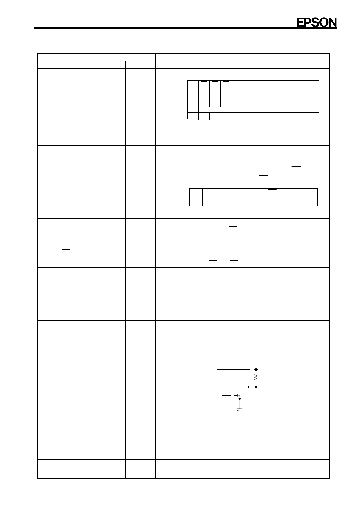
Characteristics
1. Absolute maximum ratings
Item Symbol Condition Specification Unit
Supply voltage VDD
Input voltage VI
Output voltage VO
Storage temperature T
2. Recommended operating conditions
Item Symbol Condition Specification Unit
Supply voltage VDD 4.5 to 5.5 V
Operating temperature T
Data hold voltage VDH 2.0 to 5.5 V
CS1 data hold time t
Operation recovery time tr
3. Frequency characteristics and current consumption characteristics
Item Symbol Condition Specification Unit
Frequency tolerance
Operation temperature
Frequency voltage
characteristics
Aging fa
Shock resistance S.R.
Current consumption
4. Electrical characteristics ( DC character ist ics )
Item Symbol Condition Applicable pins Min. Typ. Max. Unit
High input voltage 1 VIH1 2.2 V
Low input voltage 1 VIL1
High input voltage 2 VIH2
Low input voltage 2 VIL2
Input leakage current 1 ILK1
Input leakage current 2 ILK2
Low output voltage 1 VOL1 IOL=2.5 mA 0.4
High output voltage VOH
Low output voltage 2 VOL2 IOL=2.5 mA 0.4
Off-state leakage current I
Input capacitance CI
Input-output capacitanc e CI/O
Ta=+25 °C
Ta=+25 °C GND−0.3 to V
Ta=+25 °C GND−0.3 to V
STG
No condensation
OPR
CDR
RTC-72421
RTC-72423
See the section on data
hold timing
RTC-72421A
∆
f/f0
Ta=+25 °C
=5.0 V
V
DD
RTC-72421B
RTC-72423A
RTC-72423
RTC-72421 : −10 °C to +70 °C
(+25 °C reference)
RTC-72423 : −40 °C to +85 °C
(+25 °C reference)
Ta=+25 °C
=2.0 V to 5.5 V
V
DD
=5.0 V, Ta=+25 °C
V
DD
Drop test 3 times on a hard board from
0.75 m height, or 29400 m/ s2 × 0.2 ms ×
1/2 sin wave × 3 directions
IDD1 VDD=5.0 V 1.0 Typ. 10 Max.
I
DD
Ta=+25 °C, CS
I/O currents excluded
2
=0 V
1
V
=2.0 V 0.9 Typ. 5 Max.
DD
−
0.3 to 7.0
+0.3
DD
+0.3
DD
−55 to +85
−55 to +125
RTC-72421 ; −10 to +70
RTC-72423 ; −40 to +85
2.0 Min.
±
10
±
50
±
20
±
50
+10 / −120
+10 / −220
±
5
Max.
±
5 Max. × 10-6 / year
±
10 Max. × 10
All input pins except for
CS
OFFLK
V
DD
V
I=VDD
I
OH
VI = V
frequency
1 MHz
=2.0 V to
5.5 V
/0 V
=-400 µA
/ 0 V
DD
Input
Input pins except for
D
D
Input pins except for
D
D0 to D3 and STD.P
1
CS
1
to D3
0
to D3
0
STD.P
to D3
0
0.8
4/5VDD
1/5VDD
1/-1
10/-10
2.4
10/-10
10
20
× 10
×
10
°
°
µ
µ
V
V
V
°
C
°
C
C
C
s
-6
A
V
µ
V
µ
pF
A
A
-6
/ V
-6
Page - 4 MQ - 162 - 03
Page 8
RTC - 72421 / 72423
Switching characteristics (AC characteristics)
1. When ALE is used
Write mode ( V
Item Symbol Condition Min. Max. Unit
CS1 set-up time tSU(CS1) 1000
Address set-up time before ALE tSU(A-ALE) 50
Address hold time af ter ALE th(ALE-A) 50
ALE pulse width tw(ALE) 80
ALE set-up time bef ore write tSU(ALE-W) 0
Write pulse width tw(W) 120 ns
ALE set-up time af ter write tSU(W-ALE) 50
Data input set-up tim e before write tSU(D-W) 80
Data input hold time after write th(W-D) 10
CS1 hold time th(CS1) 1000
Write recovery t i me trec(W) 200
Read mode ( V
Item Symbol Condition Min. Max. Unit
CS1 set-up time tSU(CS1) 1000
Address set-up time before ALE tSU(A-ALE) 50
Address hold time af ter ALE th(ALE-A) 50
ALE pulse width tw(ALE) 80
ALE set-up time bef ore read tSU(ALE-R) 0 ns
ALE set-up time af ter read tSU(R-ALE) 50
Data output transfer time after read t
Data output floating transfer time after read t
CS1 hold time th(CS1) 1000
Read recovery time trec(W) 200
(1) Write mode
CS1
A0 to A3
CS0
ALE
WR
D0 to D3
(Input)
tsu(CS1)
VIH1
(2) Read mode
CS1
A0 to A3
CS0
ALE
RD
D0 to D3
(Input)
tsu(CS1)
VIH1
VIH2
tsu(A-ALE)
VIH1
VIL1
tw(ALE)
VIH2
tsu(A-ALE)
VIH1
VIL1
tw(ALE)
DD
=5 V ± 0.5 V, RTC-72421;Ta=−10 °C to +70 °C, RTC-72423;Ta=−40 °C to +85 °C )
DD
=5 V ± 0.5 V, RTC-72421;Ta=−10 °C to +70 °C, RTC-72423;Ta=−40 °C to +85 °C )
(R-Q) CL=150 pF 120
PZV
(R-Q) 0 70
PVZ
th(ALE-A)
VIH1
VIL1
VIH1
VIL1
tsu(ALE-W) tw(W)
VIH1
VIL1 VIL1
VIH1
VIL1
th(ALE-A)
VIH1
VIL1
VIH1
VIL1
tsu(ALE-R)
VIH1
VIL1 VIL1
tsu(D-W)
tpzv(R-Q)
VIH1
VIL1
th(CS1)
VIH1
th(W-D)
th(CS1)
VIH1
tpvz(R-Q)
VIH1
VIL1
tsu(W-ALE)
VIH1
VIL1
tsu(R-ALE)
VIH2
VIL1
VIH2
VIL1
Page - 5 MQ - 162 - 03
Page 9

RTC - 72421 / 72423
2. When ALE is fixed at V
Write mode ( V
Item Symbol Condition Min. Max. Unit
CS1 set-up time tSU(CS1) 1000
CS1 hold time th(CS1) 1000
Address set-up time before write tSU(A-W) 50
Address hold time af ter write th(W-A) 10 ns
Write pulse width tw(W) 120
Data input set-up tim e before write tSU(D-W) 80
Data input hold time after write th(W-D) 10
Write recovery t i me trec(W) 200
Read mode ( V
Item Symbol Condition Min. Max. Unit
CS1 set-up time tSU(CS1) 1000
CS1 hold time th(CS1) 1000
Address set-up time before read tSU(A-R) 50
Address hold time af ter read th(R-A) 10 ns
Data output transfer time after read t pzv(R-Q) CL=150 pF 120
Data output floating trans f e r t i me after read tpvz(R-Q) 0 70
Read recovery time trec(R) 200
(1) Write mode
CS1
A0 to A3
CS0
WR
D0 to D3
(Input)
(2) Read mode
CS1
A0 to A3
CS0
RD
D0 to D3
(Output)
(3) Read/write recovery mode
RD,WR
DD
VIH2
tsu(CS1)
VIH2
tsu(CS1)
DD
=5 V ± 0.5 V, RTC-72421;Ta=−10 °C to +70 °C, RTC-72423;Ta=−40 °C to +85 °C )
DD
=5 V ± 0.5 V, RTC-72421;Ta=−10 °C to +70 °C, RTC-72423;Ta=−40 °C to +85 °C )
VIH2
VIH1
VIL1
th(CS1)
VIH1
VIL1
VIH2
th(CS1)
VIH1
VIL1
VIH1VIH1
VIH1
VIL1
VIH1
VIL1
tsu(A-W)
VIH1
VIL1 VIL1
VIH1
VIL1
tsu(A-R)
VIH1
VIL1 VIL1
tpzv(R-Q)
tsu(D-W)
VOH
VOL
tw(W)
th(W-A)
VIH1
th(W-D)
th(R-A)
VIH1
tpvz(R-Q)
VOH
VOL
trec(R/W)
Page - 6 MQ - 162 - 03
Page 10

RTC - 72421 / 72423
Registers
1. Register table
Address
(Hex)
0 0 0 0 0 S1 s8 s4 s2 s1 0 to 9 1-second digit register
1 0 0 0 1 S10 * s40 s20 s10 0 to 5 10-seconds digit register
2 0 0 1 0 MI1 mi8 mi4 mi2 mi1 0 to 9 1-minute digit register
3 0 0 1 1 MI10 * mi40 mi20 mi10 0 to 5 10-minute digit register
4 0 1 0 0 H1 h8 h4 h2 h1 0 to 9 1-hour digit register
5 0 1 0 1 H10 * PM/AM h20 h10 0 to1 or 2 10-hours digit register
6 0 1 1 0 D1 d8 d4 d2 d1 0 to 9 1-day digit register
7 0 1 1 1 D10 * * d20 d10 0 to 3 10-days digit register
8 1 0 0 0 MO1 mo8 mo4 mo2 mo1 0 to 9 1-month digit register
9 1 0 0 1 MO10 * * * mo10 0 to 1 10-months digit register
A 1 0 1 0 Y1 y8 y4 y2 y1 0 to 9 1-year digit register
B 1 0 1 1 Y10 y80 y40 y20 y10 0 to 9 10-years digit register
C 1 1 0 0 W * w4 w2 w1 0 to 6 Day-of-the-week register
D 1 1 0 1 CD 30s ADJ IRQ FLAG BUSY HOLD Control register D
E 1 1 1 0 CE t1 t0
F 1 1 1 1 CF TEST 24/12 STOP RESET Control register F
A3 A2 A1 A0
Register
name
D3 D2 D1 D0
Data
ITRPT/
MASK Control register E
2. Notes
The count s at address es 0 t o C are all pos it ive logic . Theref ore, a regi st er bit t hat is 1 appears as a high-level s ignal on the dat a bus.
Data representation is BCD.
Do not set an impossi bl e date or time in the RTC. If such a value is set, the effect is unpredictable.
When the power is turned on (bef ore the RTC is initialized), the stat e of all bits i s undefined. Therefore, write to all registers after
power-on, to set initial values. For details of the initialization procedure, see "Using the RTC-72421/RTC-72423".
The TEST bit of cont rol register F is us ed by EPSON for test ing. Operation cannot be guaranteed if 1 is written to this bit, so m ake
sure that it is set to 0 during power-on initialization.
3. Functions of register bits ( overview)
Bit name Function
* mark Not used. Writing to this bit has no effect; reading it always returns 0.
Seconds to year digit All written BCD code.
This is special (base 7) counter that increments each time the day digits are incremented. It counts from 0 to 6. Since the value in the
counter bears no relationship to the day of the week, the user can choose the coding that relates the counter value to the day of the
Day-of-the-week digit
PM/AM
30-seconds ADJ Writing 1 to this bit executes a 30-seconds correction.
IRQ FLAG
BUSY
HOLD
t1,t0 These bits set the timing for fixed-period pulse output and interrupts (1/64 seconds, 1 second, 1minute or 1 hour).
ITRPT/STND
MASK
TEST
24/12
STOP
RESET
week. The following is just one example of this relationship.
Count 0 1 2 3 4 5 6
Day Sunday Monday Tuesday Wednesday Thursday Friday Saturday
The PM/AM bit is 1 for p.m. times; 0 for a.m. times. This bit is valid only for 12-hour-clock mode (when the 24/12 bit is 0); in 24-hourclock mode (when the 24/12 bit is 1), this bit is always 0.
The IRQ FLAG bit is set to 1 when an interrupt request is generated in fixed-period interrupt mode. Writing 0 to this bit clears it. Note
that it is possible to write 1 to this bit, but this will have no effect.
In fixed-period pulse output mode, this bit is at 1 while the pulse output is active(While the STD.P pin output is low), and is
automatically cleared when pulse output ends. Writing 0 to this bit while pulse output is active forcibly cancels the pulse output.
Use the BUSY bit when accessing data in the S
registers, and is set to 0 otherwise. When the BUSY bit is 1, access to the S
Note that the HOLD bit must also be used when accessing the S
There is no need to check the BUSY bit when accessing the control registers (C
When 1 has been written to the HOLD bit, the status of the BUSY bit can be checked. While the HOLD bit is 1, any incrementation of
the digits is held just once. (The incrementation is held only once, even if the HOLD bit remains at 1 for two or more seconds.)
Clear the HOLD bit to 0 by forcing the CS1 pin low.
The ITRPT/STND bit sets fixed-period pulse output mode and fixed-period interrupt mode. Write 1 to this bit to set interrupt(INRPT)
mode; when write 0 to it to set pulse output(STND) mode.
The MASK bit disables fixed-period pulse output and fixed-period interrupts. Write 1 to this bit to mask and inhibit these modes; write
0 to it to enable these modes.
The TEST bit is used by EPSON for test purposes. Operation cannot be guaranteed if 1 is written to this bit, so make sure that it is
set to 0 during power-on initialization.
The 24/12 bit switches between 24-hour clock and 12-hour clock. Write 1 to this bit to set 24-hour mode; write 0 to it to set 12-hour
mode. When the 24/12 bit is set, both the timer registers and the timer mode must be reset to match. Note that the h20 bit of the H10
register is always in 12-hour-clock mode.
The STOP bit sets an inhibition on clock operation in 8192 Hz steps which are divisions of the 1 second signal from the RTC’s
internal 32768 Hz oscillation source. The clock is inhibited when the STOP bit is 1, and released again when it becomes 0. The
internal oscillation circuit continues to operate even when the STOP bit is 1.
The RESET bit resets the part of the counter that is below one second. Write 1 to this bit to reset; 0 to release the reset.
The RESET bit set to 0 when the CS1 pin goes low.
to W registers. This bit is set to 1 during the incrementation cycle of the S1 to W
1
to W registers. The BUSY bit is always 1 when the HOLD bit is 0.
1
to W registers is inhibited.
1
, CE and CF).
D
Count
(BCD)
Remarks
Page - 7 MQ - 162 - 03
Page 11

RTC - 72421 / 72423
4. Setting the fixed-period pulse output mode and fixed-period interrupt mode
Mode
Fixed-period pulse output mode 0 0 t1 bit 0 0 1 1
Fixed-period interrupt mode 0 1
Fixed-period pulse output
inhibited
MASK ITRPT/STND ITRPT/STND STD.P
Set to 1 when
active
1 0 or 1 "0" Open-circuit Output period 1/64 s 1 s 1 min. 1 hour
Set low when
active
5. Resetting the fixed-period pulse output mode and fixed-period interrupt mode
Mode
Fixed-period pulse output mode
MASK=0
ITRPT/STND=0
Fixed-period interrupt mode
MASK=0
ITRPT/STND=1
IRQ FLAG IRQ FLAG STD.P
write 0
No write
write 0
No write The interrupt request continues, with no reset. Subsequent interrupt are ignored.
Reset immediately after the write
Automatically returned by the set period
Reset immediately after write
Setting of fixed-period output timing
pin
t0 bit 0 1 0 1
pin
Reset immediately after the write
("1" → "0")
Automatically returned by the set period
("1" → "0")
("1" → "0")
("L" → "OPEN")
("L" → "OPEN")
Reset immediately after the write
("L" → "OPEN")
Page - 8 MQ - 162 - 03
Page 12

RTC - 72421 / 72423
Register description
1. Timing registers
(1) S1 to Y10 registers
These registers are 4-bit, pos itive logic registers in which the digi ts of the year, month, day, hour, minute, and second are
continuously written in BCD code.
For example, when(1, 0, 0, 1) has been written to the bit s of the S1 register, the current value in the S1 register is 9. As
described previously, data is handled by 4-bit BCD codes. Therefore, the S 1 to Y10 registers consis t of units registers and
tens registers.
When seconds are read, for example, the values in the S1 and S 10 registers are both read out to give the t otal number of
seconds.
(2) W register
The W register is a counter that increment s eac h ti m e the day digi ts are inc rem ented. It c ounts f rom 0 to 6. S inc e the value i n
the counter bears no relationship to t he day of the week, t he user can choos e the codi ng that relat es the count er value to the
day of the week. The following is just one exampl e of this relationship;
(3) H10 register (PM/AM, h20, h10)
The H10 register contains a combination of the 10-hours digit bits and the PM/AM bit. Therefore, the cont ents of this register
will depend on whether the 12-hour clock or 24-hour clock is selec ted. If the 12-hour c lock is s elected, the us er must bear in
mind that this register will contain two types of data: 10-hour data in the h10 bit and a.m ./p.m. data in the PM/AM bit. The
PM/AM bit is 0 for a.m . and 1 for p.m.
For example, if a value of 48 is obtained f rom t he H10 and H1 registers when the H10, H1, M10, and M1 regist ers are read,
remember that the inclusion of a set PM/AM bit (PM/AM=1) will make the tens digit appear to be 4. Since this bit is 1, the t im e
is p.m. If t he val ue read from the M10 and M1 registers is 00, the actual ti me should be read as 8:00 p.m.
Similarly, if the value read from the H10 and H1 registers is 11, the P M/AM bit is 0, and so thi s time is theref ore a.m. If the
value read from the M10 and M1 registers is 30, this time should be read as 11:30 a.m .
When the 12-hour cloc k is used, the h20 bi t s hould never be 1, but it is nonet heles s physi call y pos si ble to write a 1 in thi s bit.
The user should be careful to write a 0, t o avoid unpredictable consequenc es. Note that, if a m istake in the PM/AM val ue is
made while in 12-hour-clock mode, the date digit s will be half a day out. Correct setting is needed.
If the 24-hour clock is selec ted, the PM/AM bit will always be 0.
For details of how to set 12-hour or 24-hour cloc k, see the section on the 24/12 bit.
12-hour clock 12:00 to 11:59, a.m. and p.m.
24-hour clock 00:00 to 23:59
(4) Y1 and Y10 registers
The Y1 and Y10 registers can handle the l ast two digits of the year in the Gregorian calendar.
Leap years are automatically identified, and this affect s the handling of the mont h and day digits
for February 29.
[ Leap years ]
In general, a year contains 365 days. However, the Earth takes slightly longer than exactly 365
days to rotate around the sun, so we need to set leap years in compensat ion. A leap year oc curs
once every four years, in years in the Gregorian calendar that are divisibl e by four. However, a
further small correction is neces sary in that years that are divisible by 100 are ordinary years , but
years that are further divisi bl e by 400 are l eap years.
The main leap and ordinary years since 1900 and i nto the future are listed on the right.
[ Leap years in the RTC-72421/72423 ]
To identify leap years, the RTC-72421/RTC-72423 checks whether or not the year digits are
divisible by four. As implied above, 2000 will be a leap year, and so no further correction will be
necessary in that cas e.
This process identifi es the following years as leap years:
96, (20)00, (20)04, (20)08, (20)12...
The turn-of-the-century years for which the RTC-72421/RTC-72423 will require a correction are
shown shaded in the table on the right.
If Japanese-era years are set, accurate leap-year identification will only be possible if the era
years that are divisible by four are ac tually leap years. As it happens , years in the current era,
Heisei, that are divisible by four are leap years, which means that Heisei years can be set in t hese
registers.
(5) Out-of-range data
If an impossible dat e or time is set, this m ay cause errors. If such a date is set , the behavior of the device is in general
unpredictable, so mak e sure that impossible data is not set.
Count 0 1 2 3 4 5 6
Day Sunday Monday Tuesday Wednesday Thursday Friday Saturday
Setting Possible times
Actual leap years and ordinary y ear s
Year Leap year Ordinary
1900
:
1993 Ο
1994 Ο
1995 Ο
1996
1997 Ο
1998 Ο
1999 Ο
2000
2001 Ο
2002 Ο
2003 Ο
2004
2005 Ο
:
2100
2200
2300
2400
year
Ο
Ο
Ο
Ο
Ο
Ο
Ο
Ο
Page - 9 MQ - 162 - 03
Page 13

RTC - 72421 / 72423
*
2. CD register (contro l r egister D)
(1) HOLD bit (D0)
Use the HOLD bit when accessing the S1 and W registers. For details, see "Read/write of S1 to W registers" .
HOLD bit Function HOLD bit
0 The BUSY bit is always 1 (the BUSY status cannot be checked).
1 The BUSY status can be checked. When the HOLD bits is 1 and the BUSY bit is 0, read and write are enabled.
When the HOLD bit is 1, any incrementation in the count is hel d within the RTC. The held incrementation is autom atically
compensated for when the HOLD bit becomes 0. (Second and subs equent incrementations are ignored.) Therefore, if the
HOLD bit is at 1 for two or more seconds in succession, the tim e will be slightly slow (delay). Make sure that any access t o
the S1 to W registers is completed within one second, t hen clear the HOLD bit to 0.
The status of the BUSY bit remains as set while the HOLD bit is at 1. If t he HOLD bit is not cleared temporarily to 0, the
BUSY bit will not indicate any change within the RTC of the BUSY status . Therefore, when checki ng the st atus of the BUS Y
bit, write 0 to the HOLD bit each ti me the BUSY bit is read, to update the st at us of the BUSY bit.
If the CS1 pin goes low while the HOLD bit is 1, the HOLD bit is automatically cleared to 0.
There is no need to use the HOLD bit when accessing the control registers (C
(2) BUSY bit (D1)
The BUSY bit indicates whether or not the digits from the s econds digit onward are being incremented, and is used when
accessing the S1 to W registers. For details, s ee " Read/ write of S1 to W registers".
There is no need to check the BUS Y bit when accessing the control registers (CD, CE , and CF).
BUSY bit Significance of the BUSY bit Condition Remarks
0 Access enable The RTC is not counting
1 Access disabled
1 BUSY is always 1 HOLD=0 The count cannot be checked
The status of the BUSY bit remains as set while the HOLD bit is at 1. If t he HOLD bit is not cleared temporarily to 0, the
BUSY bit will not indicate any change within the RTC of the BUSY status . Therefore, when checki ng the st atus of the BUS Y
bit, write 0 to the HOLD bit each ti me the BUSY bit is read, to update the st at us of the BUSY bit.
The BUSY bit is a read-only bit, so any attempt to write 1 or 0 to it is ignored.
(3) IRQ FLAG bit (D2)
The IRQ FLAG bit is an internal status bit that corresponds to the status of the STD.P pin output, to i ndi cate whether or not an
interrupt request has been issued to the CPU. When the STD. P pin output i s low, the IRQ FLA G bit is 1; when the STD.P pin
output is open-circuit, the IRQ FLAG bit is 0.
When writing data to the CD regi ster, keep the IRQ FLAG bit at 1, except when deliberately writing 0 to it. Writing 0 to the IRQ
FLAG bit cancels its status if it had become 1 at that instant or just before.
i. Interrupt processing (interrupt status monitor function)
Since the IRQ FLAG bit indicates that an interrupt request has been generated to the CPU, it is in synchronization with
the status of the STD.P pin output. In other words, the stat us of the S TD.P pin out put c an be m onitored by m oni toring t he
IRQ FLAG bit.
In fixed-period pulse output mode, the relationship between the IRQ FLAG bit and the STD.P pin output is as follows:
STD.P pin output IRQ FLAG bit
Low 1
Open(for open-drain output) 0
The timing of the IRQ FLAG bi t and the STD.P pin output in fixed-period pulse output mode is as follows:
STD.P pin output
HOLD=1
D
, CE, and CF).
The count has been incremented in the RTC (190 µs Max.)
IRQ FLAG bit
01 0
Approx.
1.95 ms
7.8125 ms
The output levels of the STD. P pin are low (down) and open circuit (up).
ii. STD.P pin output reset function
The STD.P pin output can be reset after an interrupt is generated by writing 0 to the IRQ FLAG bit.
The relationships of this operation are shown below. Note that writing 1 to this bit is possible, but it has no effect.
IRQ FLAG bit STD.P pin output
1 Low
0 Open(for open-drain output)
Page - 10 MQ - 162 - 03
Page 14

RTC - 72421 / 72423
*STD.P pin output
IRQ FLAG bit
The output levels of the STD. P pin are low (down) and open circuit (up).
01 0 1
Note: If the STD.P pin output rem ains low as set, subsequently generated interrupts are i gnored. In order to prevent
interrupts from being overlook ed, write 0 to the IRQ FLA G bit before the next i nterrupt is generated, to return the STD.P
pin to high.
iii. Initial setting of IRQ FLAG bit
If the fixed-period interrupt mode is not used, s et t he IRQ FLA G bit t o 1. I f t he fi xed-period interrupt m ode is us ed, s et t he
IRQ FLAG bit to 0.
(4) 30-second ADJ bit (D3)
The 30-seconds ADJ bit provides a 30-seconds correction (by which term is meant a rounding to the nearest whole minute)
when 1 is written to it. The 30-seconds c orrection takes a maximum of 76.3 µs to perform, and after the correc tion the 30seconds ADJ bit is automat ically ret urned to 0. This operation als o clears the s ub-second bits of the i nternal c ounter down t o
the 1/256-seconds counter. During the 30-seconds correcti on, acc ess to the counter regist ers at address es 0 to C is inhibi ted,
so monitor the 30-seconds ADJ bit to check that this bit has returned to 0, before starting subsequent processing. If no
access is m ade to t he RTC for 76. 3 µs or more after 1 is written to the 30-s econds A DJ bit, there is no need t o check the 30seconds ADJ bit again.
i. Operation of 30-seconds ADJ bit
Writing 1 to t he 30-seconds ADJ bit performs a 30-sec ond correction. This 30-seconds correct ion changes the seconds
and minutes digits as shown below. If the minutes digits have been incremented, an upward carry is propagated.
Status of seconds digits before correction Status of seconds digits after correction
Up to 29 seconds 00 seconds. No carry to the minutes digits.
30 to 59 seconds 0 seconds. Carry to the minutes digits.
Example: The correction caused by the 30-seconds A DJ bit set s t he ti m e within the RTC to 00: 00:00 if i t was within t he
range of 00:00:00 to 00:00:29, or to 00: 01:00 if it was within the range of 00:00:30 to 00:00:59.
ii. Access inhibited after 30-seconds correction
For 76.3 µs after 1 is written to the 30-s econds ADJ bi t, the RTC is engaged i n internal process ing, so read to and write
from the S1 to W registers is inhibited. The 30-seconds ADJ bit is automatically cleared t o 0 at the end of the 76.3 µs.
3. CE register (control r egister E)
(1) MASK bit (D0)
The MASK bit controls the S TD.P pin output. The relationships between the MASK bit, ITRP T/STND bit, and STD.P pin
output are as follows:
MASK ITRPT/STND STD.P pin output
0 0 Fixed-period pulse output mode
0 1 Fixed-period interrupt mode
1 0 or 1 Open
The timings of the MASK bit, ITRPT/STND bit, and STD.P pi n out put are as follows:
1.Fixed-period pulse output mode (ITRPT/STND=0)
MASK bit
Interrupt generation (in synchronization
with count in cre m entation)
Writing of 0 IRQ FLAG bit.
01010
IRQ FLAG bit
*STD.P pin
01 0 1 0
Nothing is output because
the MASK bit is at 1
Output timing
Automatic return
The output levels of the STD. P pin are low (down) and open circuit(up).
Page - 11 MQ - 162 - 03
Page 15

RTC - 72421 / 72423
2.Fixed-period interrupt mode (ITRPT/S TND=1)
MASK bit
1
0
0
1
IRQ FLAG bit
*STD. P pin
0
1
0
Nothing is output because
the MASK bit is at 1
Interrupt timing
Reset at the point at which 0 is written to the IRF FLAG bit
No interrupts are generated while the MASK bit is at 1
The output levels of the STD. P pin are low(down) and open circuit(up).
(2) ITRPT/STND bit (D1)
The ITRPT/STND bit specifies fixed-period pulse output m ode or fixed-period interrupt mode for the fixed-period operating
mode.
The mode selected by each setting of this bit is as follows:
ITRPT/STND Operating mode
0 Fixed-period pulse output mode
1 Fixed-period interrupt mode
For details of the tim i ng of fixed-period operation, see the section on the t0 and t1 bits below.
(3) t0 (D2), t1 (D3) bits
These bits select the timi ng of fixed-period operation in fixed-period pulse output mode or fixed-period interrupt m ode. There
is no special counter within t he RTC for fixed-period operation; the fi xed-period operation is perform ed at t he increment ation
of the time (period) spec i fied by the t0 and t1 bit s.
i. Setting t0 and t1
Setting these bits specifies the generation timing for f i xed-period puls e out put or fixed-period interrupts.
t1 t0 Period(frequency) Remarks
0 0 1/64 seconds (64 Hz)
0 1 1 second (1 Hz)
1 0 1 minute (1/60 Hz)
ii. STD.P pin output control
1 1 1 hour (1/3600 Hz)
In fixed-period pulse output mode, the STD.P pin output is low
for 7.8125 ms
(not that half the 1/64 second period is 7.8125 ms)
The timing of STD.P pi n output is at the incrementation of the peri od specified by the t0 and t1 bits.
Example : STD.P pin output when 1 hour is set
(Conditions: t0=1, t1=1, MAS K=0)
PM 1:00 PM 2:00
Fixed-period pulse output mode
STD.P pin output
(ITRPT/STND=0)
Automatic reset after 7.8125 ms
Fixed-period interrupt output mode
(ITRPT/STND=1)
iii. Frequency of STD.P pin output in fixed-period pulse output mode
In fixed-period pulse output mode, t he timing of output is determ ined by the frequency of the internal crys tal unit. This
means that the output can be used to measure any error in the frequency of the crys tal unit.
Note: The 30-seconds correction could generate a carry. If such a carry occ urs when the t0 and t1 bits are set to
(0, 1) or (1, 1), the STD.P pin output could end up low. If the ITRPT/STND bit is 0, this low-level STD.P pin output will be
held from the time that the part of the count er that is below one sec ond is cleared by the 30-s econds correc tion until t he
incrementation of t he 1/64-second digit of the internal counter restarts. Note t hat this may be different from the norm al
case in which the STD.P pin out put is low for 7.8125 ms.
The time of the low-level output of the first STD.P pin output after a RESET or STOP operation, or after 1 has been
written to the IRQ FLAG bit, may not be 7.8125 ms.
If any one of the t0, t 1, or ITRP T/STND bi ts is overwritten, the I RQ FLAG bit m ay becom e 1. Therefore, after writing t o
any of these bits, it i s necessary to first write 0 to the IRQ FLAG bit t hen wait unt i l the IRQ FLAG bit changes back to 1.
Reset by writing 0 to IRQ FLAG bit
STD.P pin output
Page - 12 MQ - 162 - 03
Page 16

RTC - 72421 / 72423
4. CF register (control register F)
(1) RESET bit (D0)
Writing 1 to the RESET bit clears the sub-second bit s of the internal counter down to the 1/256-sec onds counter. The reset
continues for as long as the RESET bit is 1. End t he reset by writing 0 to the RESET bit. If the level of the CS
the RESET bit is automatically cleared to 0.
(2) STOP bit (D1)
Writing 1 to the STOP bit st ops t he cl ock of t he internal count er from t he 1/8192 s econd bit onward. Writing 0 to the STOP bit
restarts the clock.
This function can be used t o create a cumulative timer.
(3) 24/12 bit (D2)
Set the 24/12 bit to selec t either 12-hour cl ock or 24-hour c lock as the t imer m ode. I n 12-hour cloc k m ode, the PM/AM bit is
used.
i. Switching between 12-hour clock and 24-hour clock
Writing 1 to the 24/12 bit s elect s 24-hour cloc k m ode. In 24-hour c lock m ode, t he PM/AM bit is inoperative and is always
0. Writing 0 t o the 24/12 bit select s 12-hour cloc k m ode. In 12-hour c lock m ode, t he PM/AM bit becom es valid. It is 0 for
a.m. times and 1 for p.m. times.
ii. Overwriting the 24/12 bit
Overwriting the contents of the 24/12 bit could destroy t he cont ents of t he regis ters from t he H1 regis ter upward (from the
1-hour digit upward). Therefore, before overwriting the 24/12 bit , it is necessary to save the contents of the hour (H1,
H10), day (D1, D10), month (MO1, MO10), year (Y1, Y10), and day-of-the-week (W) registers, then re-write the data back
into the registers to s ui t the new timer mode, after overwriting the 24/12 bit.
(4) TEST bit (D3)
The TEST bit is used by EPS ON for test purpos es. Operation c annot be guaranteed if 1 is writt en to t his bit , so make s ure
that it is set t o 0 duri ng power-on initi al i zat i on.
1
pin goes low,
Page - 13 MQ - 162 - 03
Page 17

RTC - 72421 / 72423
Using the RTC-72421/RTC-72423
1. Power-on procedure (initialization)
When power is turned on, the contents of all registers and the out put from t he STD.P pin are undef ined. Therefore, all the registers
must be initialized af ter power on. Follow the procedure given below for initialization.
Power On
Start the counter
Initialize the control registers
Check the status of the BUSY bit
STOP and RESET the counter
Set the current time in the registers
1
(initialize the S
Start the counter and release
the HOLD status
to W registers)
To next process
At ths point, there is no need to
(A)
check the BUSY bit.
(B)
(C)
(A)
From here on, check the status of the
BUSY bit before accessing any of the
D
registers, except for the C
control register.
For details of processes (A) to (C), see next page.
, CE and C
F
Page - 14 MQ - 162 - 03
Page 18

RTC - 72421 / 72423
(A)Starting the count
START
Set the CF register
←
←
←
←
←
0*00B
0
0 or 1
0
0
Reg.F
TEST
24/12
STOP
RESET
Set the C
This setting is not necessary when
the STD.P pin is not used
Set the C
Reg.D
30 s ADJ
IRQ FLAG
HOLD
register
E
register
D
←
←
←
←
0*00B
0
0 or 1
0
Set the IRQ FLAG bit to 0 when fixed-period
interrupt mode is used, or to 1when it is not
used.
To next process
(B) Checking the status of the BUSY bit
START
HOLD bit ← 1
Read the BUSY bit
BUSY bit=0?
YES
NO
HOLD bit ← 0
To next process
(C)Stopping and resetting the counter
START
Set the CF register
←
Reg.F
TEST
24/12
STOP
RESET 1
←
←
←
←
0*11B
0
0 or 1
1
To next process
Page - 15 MQ - 162 - 03
Page 19

RTC - 72421 / 72423
2. Read/write of S1 to W registers
Use one of the procedures shown below to acces s registers other than the control regis ters (CD, CE, and CF) while the RTC is
operating. Note that the cont rol regi sters can be accessed regardless of the status of the BUSY bit.
Read or write when the HOLD bit is used
From previous process
←
YES
set the time
←
0
1
NO
HOLD bit ← 0
Wait 190 µs
HOLD bit
Read the BUSY bit
BUSY bit = 0?
Read required digit data or
HOLD bit
or
From previous process
Read requierd digit data or
HOLD bit ← 1
Read the BUSY bit
BUSY bit = 0?
YES
set the time
HOLD bit ← 0
NO
HOLD bit ← 0
To next process
To next process
Read when the HOLD bit is not used
From previous process
Read the required digit data
(1st time)
Store the read data (A←data)
Read the required digit data
(2nd time)
Store the read data (B←data)
A=B?
YES
To next process
NO
The operation when the HOLD bit is not used involves reading the same digit twice and comparing the read values . This is to
avoid the problem of reading unstabl e data that would occur if the data was read while the RTC was incrementing the c ount .
3. Write to 30-second ADJ bit
The 30-seconds ADJ funct ion is enabled by writing 1 t o the 30-s econds ADJ bit. Note t hat t he count er regis ters (S1 to W) cannot be
accessed for 76.3 µs after this write. Therefore, f ol l ow one of t he procedures shown below to use this function.
START
30 s ADJ bit ← 1
Read the 30 s ADJ bit
or
START
30 s ADJ bit ← 1
Read the 30 s ADJ bit
30 s ADJ bit=0?
YES
END
NO
Wait 76.3 µs
30 s ADJ bit=0?
YES
END
NO
Note
The crystal unit could be damaged i f subjected to excessi ve shock. If the c rystal unit should st op operating for such a reason, the
timer within the RTC will stop. While t he crystal unit is operating, the BUSY bit is automatic ally reset every 190 µs and the 30seconds ADJ bit, every 76. 3 µs , but this automatic reset c annot be done if the os cillation st ops. Therefore, in such a st atus, it is no
longer possible to escape from the BUSY bit status chec k loop shown in subsecti on 2 above or the 30-s econds ADJ bit s tat us c hec k
loop shown in subsection 3 above, and you should consider backing up the s yst em . To des ign a fai l-saf e sys tem , provide an es cape
from the loop to a procedure that can process such an error if the loop is repeated for more than 0.5 ms to 1.0 ms.
Page - 16 MQ - 162 - 03
Page 20

RTC - 72421 / 72423
4. Using the CS
The RTC-72421/RTC-72423 has 2 chip-select s ignal systems: CS0 and CS1. Use CS0 as chip-select for ordi nary bus access.
1
CS
is not only used for CPU bus c ontrol, it also has the main functi on of switching between standby mode and operating mode.
(1) Functions
Providing the CS1 pin with the rated voltage levels enables CS1 to have the following functions:
•
Enabling interface with mi croprocessor during operation within the operating voltage range (5.0 V ±0.5 V)
•
Reducing current consum ption during standby (to prevent t hrough currents caused by uns table inputs, which i s inherent to
C-MOS devices)
•
Protecting internal data during standby
To ensure these functions, make sure that operation of the CS1 pins observes that following conditions:
•
Make sure that the voltage input to the CS
•
Make sure that the voltage input to the CS
•
Make sure that the operation conforms to t he timing chart below during a shift to st andby mode or a return to operating
mode.
* Standby mode is a stat e in which a voltage lower than t he RTC's rated range of operati ng supply voltage is applied (4.5 V
to 2.0 V). Under this condit ion, the timer continues to operat e under battery back-up power, but the interface between the
interior and exterior of the RTC cannot be guaranteed.
(2) Timing
(3) Note
If the RTC is operated with tim ing conditions different from thos e shown above, data within the RTC could be overwritten
during a shift to standby m ode or a ret urn to operat ing m ode. For exampl e, if a write signal (WR) is generated during ei ther of
the timing conditions (tCDR, tR) shown in the tim ing chart above, the data will be input before the RTC has stabilized. To
ensure that data is held throughout the entire standby process , make sure that t he timing conditions shown in the chart are
followed.
pin
1
Shift to standby mode Return to operation mode
4 V4 V
CDR
t
Min.
2 µs
IL2
V
(1/5 VDD)
Power supply circuit example
+5 V
1
pin during operation is at least 4/5 VDD.
1
pin during standby is as close as possible to 0 V, to prevent through currents.
Data hold mode
Must be at least 2.0 V
Must be at no more than 1/5 V
Do not access the RTC while the voltage at CS1 is changing.
DD
t
Min.
2 µs
IH2
V
(4/5 VDD)
R
Note1 Note2
+
DD
V
Voltage
detection
circuit
Ceramic capacitor of
RTC
CS1
0.01 µF to 0.1 µF
GND
Note 1:This capacitor must be of a high capacity because a transi ent reverse current flows from the collector to the emitter of the
transistor when the power is turned off.
Note 2:Use a chargeable or lithium battery. If a chargeable battery is used, t here i s no need for the diode. If a lithium battery is used,
the diode is necessary. For specific details of the resist ance of the resistor, contact the manufacturer of the battery that is used.
Page - 17 MQ - 162 - 03
Page 21

RTC - 72421 / 72423
Examples of connection to general-purpose microprocessor
When connecting the RTC-72421/RTC-72423 to a microprocessor, carefully check the AC timings of both the RTC and the
microprocessor.
1. Connection to multiplexed bus type
8085/MCS48,51 RTC-72421/3
AD3
AD2
AD1
AD0
Upper address bus
Decoder
IO/M
ALE
A3
A2
A1
A0
D3
D2
D1
D0
CS0
ALE
8085/MCS48,51 RTC-72421/3
AD3
AD2
AD1
AD0
Upper address bus
Decoder
IO/M
ALE
Latch
A3
A2
A1
A0
D3
D2
D1
D0
CS0
ALE
RD
WR
RD
WR
RD
WR
The resistors on the RD and WR lines are not necessary if the CPU does not have a HALT or HOLD state.
2. Connection to Z80 or compatible CPU
Z80, SMC84C00AC RTC-72421/3
A3
A2
A1
A0
D3
D2
D1
D0
Upper address bus
IORQ
or
MEMRQ
RD
WR
Decoder
*Select IORQ or MEMRQ depending on whether the RTC maps I /O or memory of the CPU.
A3
A2
A1
A0
D3
D2
D1
D0
CS0
ALE
RD
WR
3. Connection to 68-series MPU
68 series MPU RTC-72421/3
A3
A2
A1
A0
D3
D2
D1
D0
Upper address bus
Decoder
A3
A2
A1
A0
D3
D2
D1
D0
CS0
ALE
RD
WR
R/W
E
RD
WR
Page - 18 MQ - 162 - 03
Page 22

RTC - 72421 / 72423
External dimensions
1. RTC-72421
2. RTC-72423
1.52
0.46
23.1 Max.
16.3 Max.
2.54
0.2
Min.
6.3
4.2
Max.
2.54
Min.
0 - 15
7.62
0.25
Marking layout
Type
RTC72421
EPSONA6053C
0.35
7.9
0.1
Min.
1.27
Frequency tlerance
2.8
Max.
0 - 10
Unless otherwise stated, al l uni ts are [mm]
Indications of frequency tolerance
Type Tolerances
RTC-72421
RTC-72423
Indication
A
B
A
No indications
12.0
±
10 x10
±
50 x10
±
20 x10
±
50 x10
0.2
1.0
-6
-6
-6
-6
Logo mark
Note: The illustration is a general representation of the content and locati on of information on the
label, and is not a detailed specification of the typefac e, size or positioning of printi ng used on the
label.
Manufacturing lot no.
Page - 19 MQ - 162 - 03
Page 23

RTC - 72421 / 72423
6
Reference data
1. Example of frequency and temperature characteristics
= +25 °C Typ.
T
-
]
θ
= -0.035 × 10
α
Temperature [°C]
-6
Typ.
Condtions
5 V reference,Ta=+25 °C
-6
× 10
0
T
f
∆
-50
-100
Frequency
-150
-50 0 +50 +100
2. Frequency voltage characteristics ( Typ. )
Frequency[x10
+4
[Finding the frequency stability]
1. Frequency and temperature charac teristics can be approximated
using the following equations.
∆fT = α ( θT - θX )2
∆
fT
α
( 1 / °C2 )
θ
T ( °C )
θ
X ( °C )
2. To determine overall cloc k accuracy, add the frequency precision
and voltage characteristi cs.
∆f/f = ∆f/fo + ∆fT + ∆fV
∆
f/f
∆
f/fo
∆
fT
∆
fV
3. How to find the date difference
Date Difference = ∆f/f × 86400(s)
* For example: ∆f/f = 11.574 × 10⁻⁶ is an error of
approximately 1 second/day.
3. Current consumption vol tage characteristics ( Typ. )
: Frequency deviation in any
temperature
: Coefficient of s econdary temperature
−
(
0.035±0.005 ) × 10-6 / °C2
±
: Ultimate temperature (+25
: Any temperature
: Clock accuracy (s table frequency) in
any temperature and voltage.
: Frequency precision
: Frequency deviation in any
temperature.
: Frequency deviation in any voltage.
5 °C)
Current consumpti on[µA]
Conditions
5
CS1=0 V, No load, Ta=+25 °C
+2
4
6 2 3 4 5
0
-2
Supply Voltage(VDD) [V]
-4
3
2
1
62345
Supply voltage(VDD)
Note: This data shows average values for a sample lot.
For rated values, see the specifi cations.
Page - 20 MQ - 162 - 03
Page 24

RTC - 72421 / 72423
s
s
Application notes
1. Notes on handling
This module uses a C-MOS IC to realize low power consumption. Carefully note the following cautions when
handling.
(1) Static electricity
(2) Noise
(3) Voltage levels of input pins
(4) Handling of unused pins
2. Notes on packaging
(1) Soldering heat resistance
(2) Mounting equipment
(3) Ultrasonic cleaning
(4) Mounting orientation
(5) Leakage between pins
Fig. 1: Example GND Pattern
RTC-72421
RTC-72423
While t his module has built-i n circ uitry des igned to prot ect it against electr ostat ic di scharge, the c hip c ould st ill be
damaged by a large discharge of static electricity. Containers used for packing and transport should be
constructed of conductive materials. In addition, only soldering irons, measurement circuits, and other such
devices which do not l eak high voltage should be used with this module, which should also be gr ounded when
such devices are being used.
If a signal with exces s ive exter nal noi s e is appli ed t o the power suppl y or input pins , the devi ce may mal func ti on or
"latch up." In order t o ensur e stabl e operati on, connec t a fi lter capac itor (pref erably c eramic ) of gr eater t hat 0.1 µF
as close as possibl e to the power supply pins ( between V
generates high level of electronic noise near this module.
∗
Do not connect signal lines to the s haded area in t he figur e shown in Fi g.1 and, i f pos sibl e, embed t his area in a
GND land.
Apply signal levels that ar e as close as possible to VDD and ground, to all pins except the CS1 pin. Mid-level
potentials will cause increased current consumption and a reduced noise margin, and can impai r the f uncti oning of
the device.
Since it is likely that power consumption will increase excessively and operation cannot be guaranteed, t he s etti ng
of the voltage range of V
affected by rippl e or other noise.
Note that the CS1 pin cannot handle a TTL interface.
Since the input impedanc e of the signal pins i s extremely high, operating the devi ce with thes e pins open ci rcuit
can lead to malfunct ions due t o noise. Pull- up or pull -down res is tors should be pr ovided for all unused signal pins .
The N.C. pins should be c onnected to either V
directly to V
DD
.
If the temperature within the package exceeds +260 °C, the characteristics of the crystal oscillator will be degraded
and it may be damaged. The reflow conditions within our reflow profile is recommended.
Therefore, always check the mounting temperature and time befor e mounting this devi ce. Also, check again if the
mounting conditions are later changed.
∗
See Fig.
2 profile for our evaluation of Soldering heat resis tance for reference.
While thi s module can be used with general-pur pose mounting equipment, the internal crystal oscillator may be
damaged in some circums tanc es , depending on t he equipment and c ondit ions . Theref or e, be s ure t o c heck thi s . I n
addition, if the mounting conditions are later changed, the same check should be perform ed again.
Depending on the usage conditi ons, there is a possibility that the crystal oscillator will be damaged by resonance
during ultrasonic cl eaning. Since the condit ions under which ultr asonic cleaning is carr ied out (t he type of cl eaner,
power level, time, s tate of the i nside of the cl eaning vessel, etc.) var y widely, this device is not warranted against
damage during ultrasonic cleaning.
This device can be damaged if it is mount ed in the wrong or ientati on. Always c onfirm the or ientati on of the device
before mounting.
Leakage between pins may occur if the power is t urned on while the device has condensati on or dirt on it. Mak e
sure the device is dry and clean before supplying power to it.
IH2
and V
DD
and GND ). Also, avoid plac ing any device that
IL2
at the CS1 pin should be suc h that the system is designed so that it i s not
DD
or GND, to prevent noise. If not using the ALE pin, connect it
Fig. 2 Reference prof ile for our evaluation of Soldering heat resistance.
T em perature [ °C ]
+1 ∼ +5 °C /
Pre-heating area
+1 ∼ +5 °C /
+170 °C +220
100 s
+260 °C Max.
C
°
35 s
Stable Melting are a
−1 ∼ −5 °
C / s
time [ s ]
Page - 21 MQ - 162 - 03
Page 25

Application Manual
Distributor
AMERICA
EPSON ELECTRONICS AMERICA, INC.
HEADQUARTER 150 River Oaks Parkway, San Jose, CA 95134, U.S.A.
Phone: (1)800-228-3964 (Toll free) : (1)408-922-0200 (Main) Fax: (1)408-922-0238
http://www.eea.epson.com
Atlanta Office 3010 Royal Blvd. South, Ste. 170, Alpharetta, GA 30005, U.S.A.
Phone: (1)877-332-0020 (Toll free) : (1)770-777-2078 (Main) Fax: (1)770-777-2637
Boston Office 301Edgewater Place, Ste. 120, Wakefield, MA 01880, U.S.A.
Phone: (1)800-922-7667 (Toll free) : (1)781-246-3600 (Main) Fax: (1)781-246-5443
Chicago Office 101 Virginia St., Ste. 290, Crystal Lake, IL 60014, U.S.A.
Phone: (1)800-853-3588 (Toll free) : (1)815-455-7630 (Main) Fax: (1)815-455-7633
El Segundo Office 1960 E. Grand Ave., 2nd Floor, El Segundo, CA 90245, U.S.A.
Phone: (1)800-249-7730 (Toll free) : (1)310-955-5300 (Main) Fax: (1)310-955-5400
EUROPE
EPSON EUROPE ELECTRONICS GmbH
HEADQUARTER Riesstrasse 15, 80992 Munich, Germany
Phone: (49)-(0)89-14005-0 Fax: (49)-(0)89-14005-110 http://www.epson-electronics.de
Düsseldorf Branch Office Altstadtstrasse 176, 51379 Leverkusen, Germany
Phone: (49)-(0)2171-5045-0 Fax: (49)-(0)2171-5045-10
UK & Ireland Branch Office Unit 2.4, Doncastle House, Doncastle Road, Bracknel l, Berkshire RG12 8PE, England
Phone: (44)-(0)1344-381700 Fax: (44)-(0)1344-381701
French Branch Office LP 915 Les Conquérants, 1 Avenue de l' Atlantique, Z.A. de Courtaboeuf 2
91976 Les Ulis Cedex, France
Phone: (33)-(0)1-64862350 Fax: (33)-(0)1-64862355
ASIA
EPSON (CHINA) CO., LTD.
23F, Beijing Silver Tower 2# North RD DongSangHuan ChaoYang District, Beijing, China
Phone: (86) 10-6410-6655 Fax: (86) 10-6410-7319 http://www.epson.com.cn
4F, Bldg.,27, No.69, Gui Qing Road, Cao hejing, Shanghai, China
Phone: (86) 21-6485-0835 Fax: (86) 21-6485-0775
EPSON HONG KONG LTD.
20/F., Harbour Centre, 25 Harbour Road, Wanchai, Hong kong
Phone: (852) 2585-4600 Fax: (852) 2827-2152 http://www.epson.com.hk
EPSON ELECTRONIC TECHNOLOGY DEVELOPMENT (SHENZHEN )CO., LTD.
Flat 16A, 16/F, New Times Plaza, No.1 Taizi Road, Shenzhen, China
Phone
EPSON TAIWAN TECHNOLOGY & TRADING LTD.
14F, No.7, Song Ren Road, Taipei 110
Phone: (886) 2-8786-6688 Fax: (886)2-8786-6660 http://www.epson.com.tw
EPSON SINGAPORE PTE. LTD.
No.1, Temasek Avenue #36-00, Millenia Tower, Singapore 039192
Phone: (65) 337-7911 Fax: (65) 334-2716 http://www.epson.com.sg
SEIKO EPSON CORPORATION KOREA Office
50F, KLI 63 Building,60 Yoido-dong, Youngdeungpo-Ku, Seoul, 150-763, Korea
Phone: (82) 2-784-6027 Fax: (82) 2-767-3677 http://www.epson-device.co.kr
Gumi Branch Office 6F, Good Morning Securities Bldg., 56, Songjeong-dong Gumi-City, Gyongsangbuk-Do,
730-090, Korea
Phone: (82) 54-454-6027 Fax: (82) 54-454-6093
: (86) 755-6811118 Fax: (86) 755-6677786
ELECTRONIC DEVICE MARKETING DEPARTMENT
Electronic devices information on WWW server
http://www.epsondevice.com
 Loading...