

Page 1
EPSON
EPSON PhotoPC 500
SERVICE MANUAL
DIGITAL CAMERA
SEIKO EPSON CORPORATION
Rev.A
4006988
Page 2

NOTICE
All rights reserved. Reproduction of any part of this manual in any form whatsoever
without SEIKO EPSON’s express written permission is forbidden.
The contents of this manual are subjects to change without notice.
All efforts have been made to ensure the accuracy of the contents of this manual.
However, should any errors be detected, SEIKO EPSON would greatly appreciate
being informed of them.
The above notwithstanding SEIKO EPSON can assume no responsibility for any
errors in this manual or the consequences thereof.
Epson is a registered trademark of Seiko Epson Corporation.
General Notice:
Other product names used herein are for identification purposes only and may be
trademarks or registered trademarks of their respective companies.
Copyright 1996 by SEIKO EPSON CORPORATION
Nagano, Japan
ii
Page 3

PRECAUTIONS
Precautionary notations throughout the text are categorized relative to 1) personal injury and 2)
damage to equipment.
DANGER
WARNING
The precautioary measures itemized below should always be observed when performing
repair/maintenance procedures.
Signals a precaution which, if ignored, could res ult in ser ious or f atal per sonal injury.
Great caution should be exercised in perfor ming procedures pr eceded by DANGER
Headings.
Signals a precaution which, if ignored, could result in damage to equipment.
DANGER
1. ALWAYS DISCONNECT THE PRODUCT FROM BOTH THE POWER SOURCE AND
PERPHERAL DEVICES PERFORMING ANY MAINTENANCE OR REPAIR PROCEDURES.
2. NO WORK SHOULD BE PERFORMED ON THE UNIT BY PERSONS UNFAMILIER WITH
BASIC SAFETY MEASURES AS DICTATED FOR ALL ELECTRONICS TECHNICIANS IN
THEIR LINE OF WORK.
3. WHEN PERFORMING T ESTING AS DICTAED W ITHIN T HIS MANUAL. DO NOT CONNECT
THE UNIT TO A POW ER SOURCE UNTIL INSTRUCTED TO DO SO. W HEN THE POW ER
SUPPLY CABLE MUST BE CONNECTED, USE EXTREME CAUTION IN WORKING ON
POWER SUPPLY AND OTHER ELECTRONIC COMPONENTS.
WARNING
1. REPAIRS ON EPSON PRODUCT SHOULD BE PERFORMED O NLY BY EPSON CERTIFIED
REPAIR TECHNICIAN.
2. MAKE CERTAIN THAT T HE SOURCE VOLT AGE IS THE SAME AS T HE RATED VOLT AGE,
LISTED ON THE SERIAL NUMBER/RATING PLATE. IF THE EPSON PRODUCT HAS A
PRIMARY AC RATING DIFFERENT FROM AVAILABLE POWER SOURCE, DO NOT
CONNECT IT TO THE POWER SOURCE.
3. ALWAYS VERIFY THAT T HE EPSON PRODUCT HAS BEEN DISCONNECT ED FROM THE
POWER SOURCE BEFORE REMOVING OR REPLACING PRINTED CIRCUIT BOARDS
AND/OR INDIVIDUAL CHIPS.
4. IN ORDER TO PROTECT SENSIT IVEMICROPROC ESSORS AND CIRCUIT RY, USE STAT IC
DISCHARGE EQUIPMENT, SUCH AS ANTI-ST ATIC WRIST ST RAPS, WHEN ACCESSING
INTERNAL COMPONENTS.
5. REPLACE MALFUCNTIONING COMPONENTS ONLY WITH THOSE COMPONENTS BY
THE MANUFACTURE; INTRODUCTION OF SECOND-SOURCE ICs OR OTHER
NONAPPROVED COMPONENTS MAY DAMAGE THE PRODUCT AND VOID ANY
APPLICABLE EPSON WARRANTY.
iii
Page 4
REVISION STATUS
Revision Issued Data Contents
Rev A October 29,1996 1st issued
EPSON OVERSEAS MARKETING LOCATIONS
EPSON America, Inc
20770 Madrona Avenue,
P.O. Box 2842
Torrance, CA 90509-2842
Phone: (800)922-8911
Fax: (310)782-5220
EPSON UK LTD.
Campus 100, Maylands Avenue,
Hemel Hempstead, Herts, HP2 7TJ
U.K.
Phone: 1442-61144
Fax: 1442-227227
EPSON IBERICA, S.A.
Avda. de Roma, 18-26
08290 CERDANYOLA DEL VALLES
Balcerona, Spain
Phone: 582.15.00
Fax: 582.15.55
EPSON AUSTRALIA PTY. LIMITED
1/70 Gibbes Street,
Chatswood 2067 NSW
Australia
Phone: 02-415-9000
Fax: 02-417-0077
EPSON HONG KONG LTD.
20/F, Harbour Centre,
25 Harbour Road, Wanchai, HONG KONG
Phone: 585-4600
Fax: 827-4346
SEIKO EPSON CORPORATION
Imaging & Information Products Division
EPSON DEUTCHLAND GmBH
Zülpicher Straße 6, 4000 Düsseldorf 11
F.R. Germany
Phone: 0211-56030
Fax: 0211-504-7787
EPSON FRANCE S.A.
68 bis, rue Marjolin 92300,
Levallois-Perret
France
Phone: 1-4087-3737
Fax: 1-4737-1510
EPSON ITALIA S.p.A.
V. le F. lli Casiraghi, 427
20099 Sesto S. Giovanni (MI)
Italy
Phone: 02-26233-1
Fax: 02-2440705
EPSON SINGAPORE PTE. LTD.
NO.1 Raffles Place #26-00
OUB Centre
Singapore 0104
Phone: 5330477
Fax: 5338119
EPSON TAIWAN TECHNOLOGY &
TRADING LTD.
10F, No. 287 Nonking E. Road, Sec. 3,
Taipei, Taiwan, R.O.C.
Phone: 2-717-7360
Fax: 2-712-9164
80 Harashinden, Hirooka, Shiojiri-Shi, Nagano-Ken 399-07 JAPAN
Phone: 0263-52-2552
Fax: 0263-54-4007
iv
Page 5

As of July, 1996
v
Page 6

HAPTER
C
1. P
RODUCT DESCRIPTION
................................................................................................
...............................................................................................................1.2. Specifiation2
.............................................................................................
..........................................................................................................1.2.2. Environmental conditions4
...............................................................................................................1.2.3. Electrical Specification4
..........................................................................................................1.2.4. Safety Standards and EMI4
.....................................................................................................................................1.2.5. Reliability5
.................................................................................................................1.2.6. Operating Conditions5
.............................................................................
................................................................................................
...................................................................................
.....................................................................................................
....................................................................................................................................1.4.2. LCD Panel9
...............................................................................................................................1.4.3. LED Indicator10
......................................................................................................1.4.4. Buttons on the LCD monitor11
.......................................................................................................................1.4.5. Functional Setting12
....................................................................................
1.2.1. General specification2
1.3. Interface Specification5
1.3.1. Cable Specification6
1.4. Camera Operation8
1.5. Main Component13
1.1. Features1
1.4.1. Control buttons8
.1.
Page 7
.2. Features
PhotoPC 500 is the digital still camera that has high image quality but inexpensive for its high
performance.
The major camera features are;
* The Table 1-1 shows printable photos with optional memories and the figure below shows exterior view
of PhotoPC 500.
High Image Quality
VGA (640 x 480 pixels, 24bit color)
Sensor
Color Area CCD (Progressive Scan type)
Focus
Fixed
Exposure
Automatic
Internal memory
2MB (for image and firmware)
Built-in-Flash
4 mode : Auto/No-red eyes Auto/Off/Forced flash
Power
AA-size batteries (Alkaline/Ni-Cadium/Lithium)
Size
20% Smaller than CP-100
Interface
High Speed Serial interface : 19200bps (min.)1 15.2Kbps (max.)
Option
Expand Memory 2/4MB (See Table 1-1)
AC adapter
LCD monitor
Camera control is available from the PC.
Various filters and lenses for 37mm video camera can be attached to the front lens.
Table 1-1. Optional Units
Unit Model No.
Expansion Memory module (2MB) B808201
Expansion Memory module (4MB) B808211
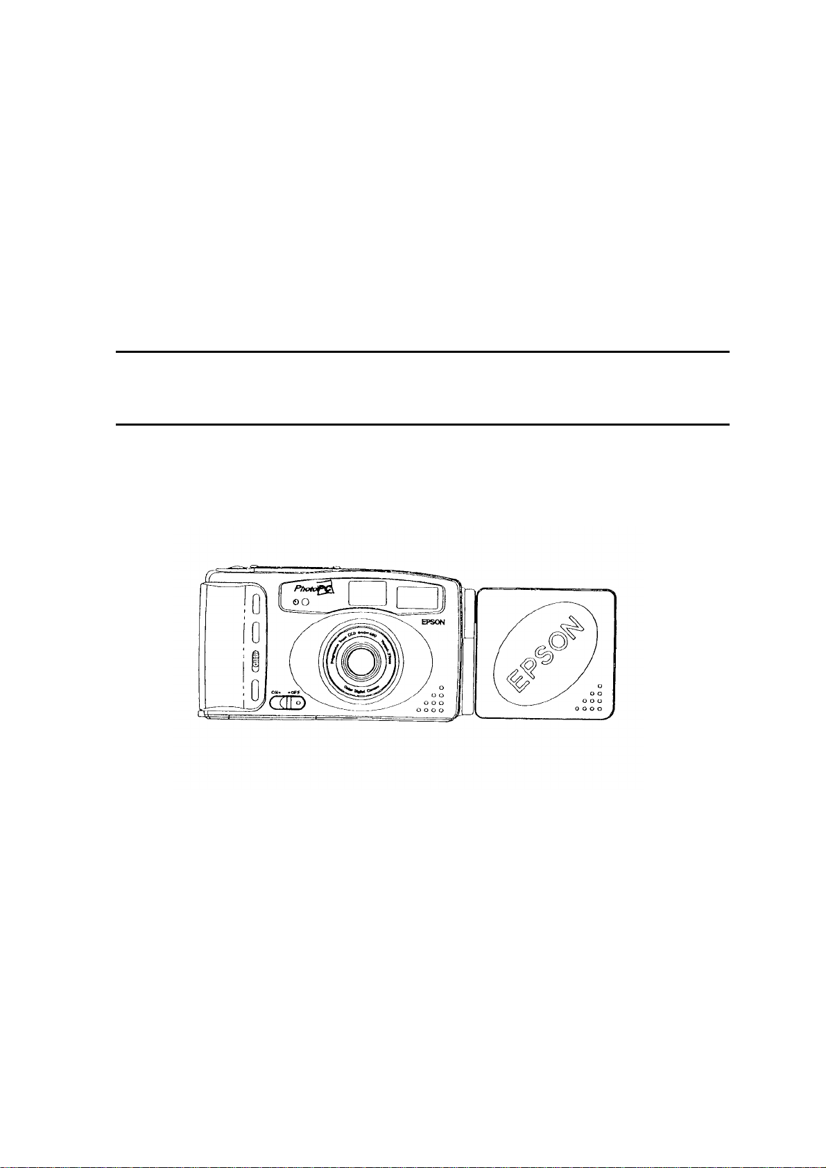
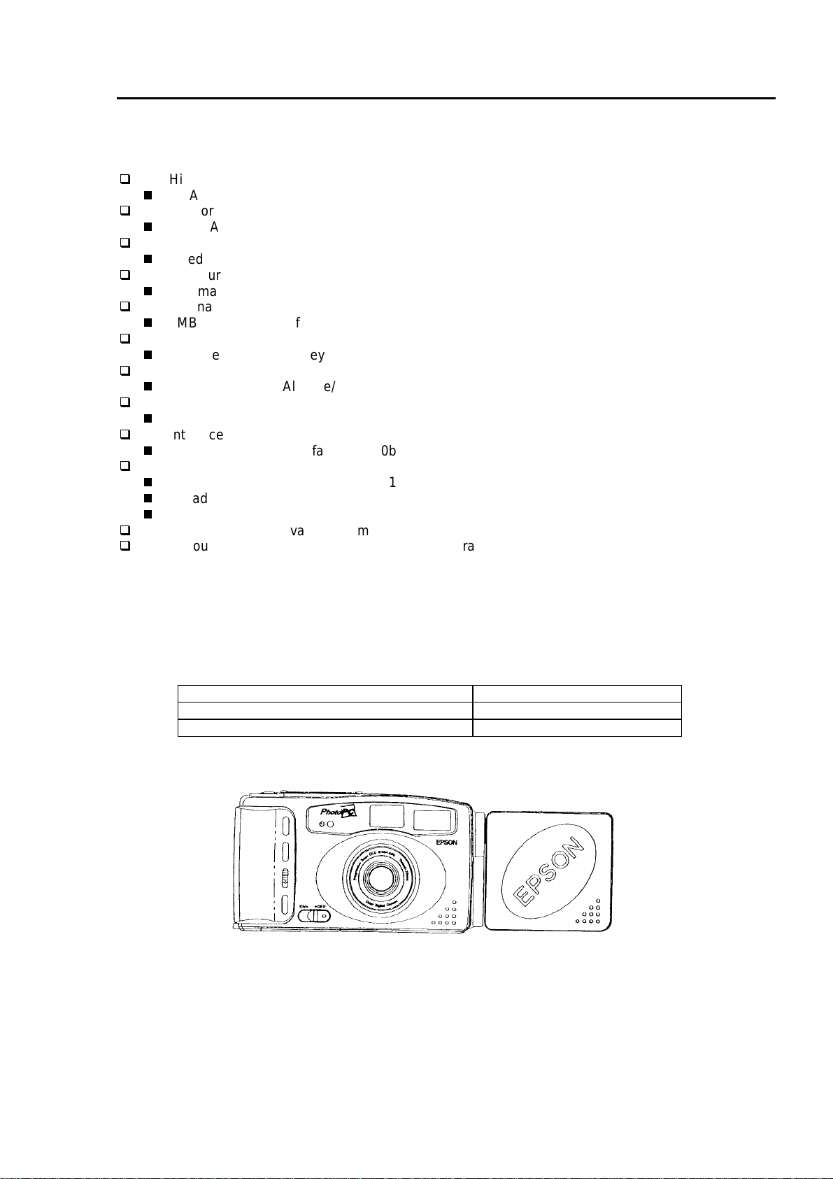
Figure 1-1. Exterior of PhotoPC 500
Page 8
PHOTOPC 500 SERVICE MANUAL Service Manual
.3. Specifiation
This section describes detailed specifications of the camera.
1.
[ Recorded Image]
High resolution 30 65 100
Standard resolution 60 130 200
General specification
Internal memory : 2MB (including approx.300KB Program Area)
Expandable Memory : Expandable Memory Module 2MB/4MB(Same as CP-100)
Compression : JPEG
File Format : JPEG. Including thumbnail (H80xV64 pixels), Date and time
information
Resolution : High resolution 640 x 480 pixels
: Standard resolution 320 x 240 pixels
White Balance : Automatic adjustment
Sensitivity : ISO 130 equivalent
Color : 24bit Full Color (8bit pixel x3)
Processing Time : High resolution Approx. 6 sec
Standard resolution Approx. 2 sec
* Red LED on side of viewfinder will flash during processing.
Number of images with Expandable Memory Module (see below Table 1-2)
Table 1-2. Printable photos with memory
Default +2MB +4MB
[CCD]
[Lens]
[Viewfinder]
[Shutter]
While connecting to PC, you can adjust from Application. But it
returns to Automatic mode after disconnecting from PC.
[Iris]
Feature : 1/3» ICX084AK (SONY) Square pixel
Total Pixels : 692(H) x 504(V) Approx. 350K pixels
Available Pixels : 659(H) x 494(V) Approx. 330K pixels
Transfer : Progressive scan type
Focus Distance : 6mm equivalent to 43mm lens on a 35mm camera
Aperture Ratio : 1:2.8
Focus range : 60cm infinity (Flash available by 3.0m)
20cm infinity (available with LCD monitor)
Structure : 5 set 5 pieces
Type : Optical Virtual Image
Magnification : x0.65
Indicator in Viewfinder : Guide Frame
Method : Electronic shutter
Exposure : Automatic 1/30 1/10000 sec.
2
Rev. A
Page 9
3
Method
is
[Exposure Control]
Method : Exposure control by iris-Shutter change program (Automatic)
[Measurement]
Chapter 1 Product Description
:
Fixed mechanical iris F2.8/F8 (When the optional LCD monitor
installed, F8 is fixed at close distance photo mode)
Method : Center-prioritized light measurement
Sensor : As both for CCD image capturing sensor
[Built-in Flash]
Type : Fixed Built-in Flash
Mode : Auto/ No red-eyes Auto/Off/Forced flash
Exposure Control Method : Automatic Luminance Control by Pre-flash
Color temperature : 5500K degree
Distance : 0.45m3m
Guide number : G No 8.4 (ISO100 Equivalent) G No 9.6 (ISO130 Equivalent)
[Self-Timer]
Time : 10 sec. (cancelable by pushing timer switch)
[Power]
Main power supply : AA Alkaline x 4 or
Battery Life : > 200 pictures (without LCD monitor, 50% flash, Alkaline
AC adapter : Optional
: Auto/ No red-eyes Auto:Auto flashing against low brightness and
backlight
AA Ni-cd x 4 or
AA Ni- MH x 4 or
AA Lithium x4
* Mixing different type of batteries are not acceptable.
* Can not charge Ni-Cd or Ni-MH by camera.
* Battery life indicator is useful only on Alkaline Battery.
Battery)
[External interface]
DC input : NewEIAJ Type3, 5.5mm diameter, center plus
Output : RS232C, Mini Din 8pin
LCD monitor adapter terminal : yes
[Date/Time]
Recording Method : Digital data recorded in file
(year/month/day/time/minute/second)
Date/Time Setting : Only adjustable from PC
Back up : Date and Time will be cleared when batteries are dead or
after the batteries are replaced exchanging.
[Erase]
All Erase : Camera: Erase+Selftimer button
PC : From Application
Erase one image : Camera: Erase for last image
LCD Monitor attached allows to erase selected one.
PC : Selected image erasable from Application
Erase Time : All erase <10 sec. (When no Expand Memory)
Erase one image < 0.5 sec.
Rev. A
Page 10

PHOTOPC 500 SERVICE MANUAL Service Manual
4
[Sound]
[Auto Shut Off]
PhotoPC 500 goes to Power Save mode under following conditions.
Camera only : Default 1min (Adjustable from PC Application)
Connecting with PC : Default 5min (Not adjustable)
Using AC adapter : No power saving
[Others]
Beep sound : After picture is taken and during image processing. (Once:pi)
Error beep sound occur when pushing shutter during image
processing. (Twice:pipi)
Without LCD Monitor
With LCD Monitor
View Mode : Camera On as same as camera only
Camera Off Turn Off 10 sec. after warming sign
Playback Mode : Default 5min (Not adjustable)
To return from Power saving : Push the Shutter button
Screw for tripod : Yes
37mm thread for additional lens or filter available
[Exterior]
2.
[Acceptable environment]
3.
Max.: DC 8V
4.
EN61000-3-3,
EN55082-1
IEC801-2
Dimensions : 141.2 (W) x 81 (H) x 52.6 (D) mm (Camera only)
221.5 mm x 81mm x 60.6 mm ( With the optional LCD monitor )
Weight : Under 300g (Without batteries, without LCD monitor)
Environmental conditions
Temperature Operating : 0 to 40 degree
Storage : -20 to 60 degree
Humidity Operating : 30 to 90% no condensation
Storage : 10t o 90% no condensation
Electrical Specification
Requirement of supply voltage for DC input (AC adapter)
Min.: DC 6.3V
Absolute maximum supply voltage for DC input
Max.: DC 10V
Safety Standards and EMI
USA : FC Class B
Europe : EN55022 Class B,
EN61000-3-2,
IEC801-3
IEC801-4
Rev. A
Page 11

Chapter 1 Product Description
5.
6.
Place : Ordinary home, office or outside
Reliability
FLASH memory life : 10K cycle write for FLASH memory
Operating Conditions
.4. Interface Specification
PhotoPC 500 can be connected to the PC only by the serial interface(RS-232C compatible).
The minimum s peed requirem ent of serial inter fac e of PC is 19200bps . T his sec tion descr ibes the use of
serial interface and cable.
[Serial Interface]
Data format: RS-232C
Communication method: Asynchronous. 8bit, Non Parity
Speed: 19200,38400,57600,115200 bps
Rev. A
5
Page 12
PHOTOPC 500 SERVICE MANUAL Service Manual
6
1.
This section describes DOS/V connector cable and conversion connector for Mac.
3
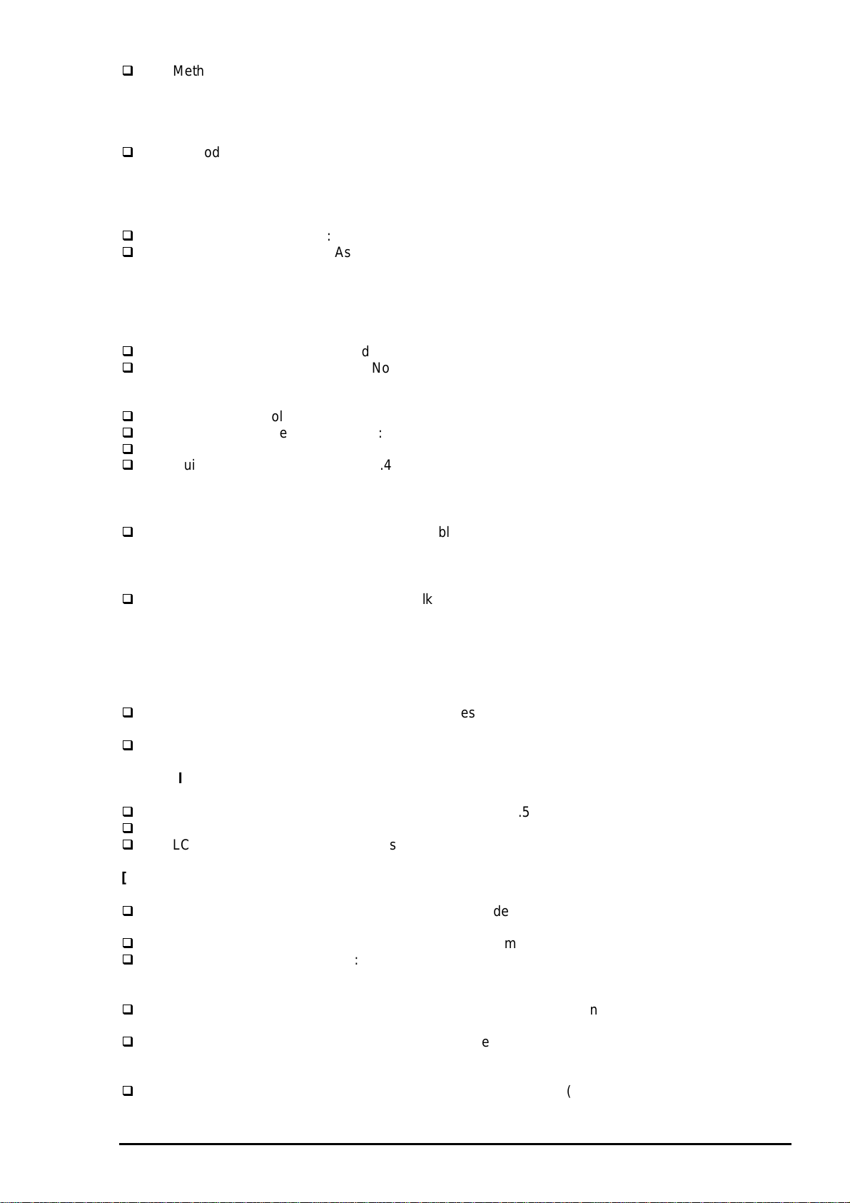
[Cable/connector description 1: DOS/V Cable]
The following figure shows the connection diagram of DOS/V cable.
Cable Specification
7
6
4
8
5
2
1
Figure 1-2. Cable for PC
1
2
3
4
5
6
7
8
9
Figure 1-3. Connection for diagram for DOC/V cable
Rev. A
Page 13
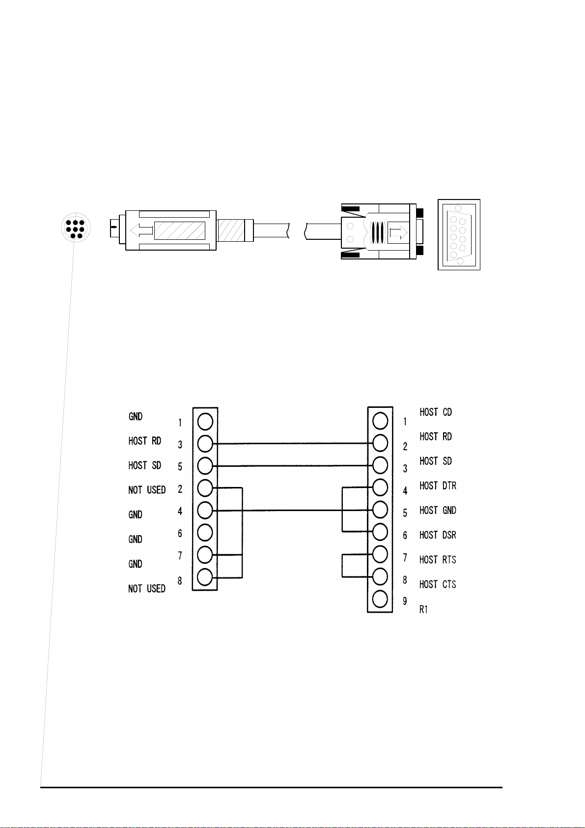
[Cable/Connector description 2: MAC adapter]
7
6
4
3
8
5
2
1
Figure 1-4. Mac adapter
Chapter 1 Product Description
1
2
3
4
5
6
7
8
9
The following figure shows the connection diagram of MAC Cable.
Figure 1-5. Connection for Mac cable
Rev. A
7
Page 14

PHOTOPC 500 SERVICE MANUAL Service Manual
8
.5. Camera Operation
This section describes LCD panel display and its functions.
1.
The LCD panel consist of 5 buttons and displays the camera operation. The power s witch is loc ated under
the lens and move along with the closing and opening movement of shutter. The following Figure1-6
shows
these 5 buttons on the LCD Panel and their functions.
Control buttons
Figure 1-6. Control buttons
Button A
*
Button B:
*
Button C:
*
Button D:
*
Button E:
*
: Shutter Button. Photo shooting.
Erase button. Function is different according to the following conditions.
*Without LCD monitor : erase last image
* With LCD monitor :
Playback mode : erase displayed image
Off or View mode : erase last image
*All images erase : push Self-Timer button while pressing Erase button
Flash mode button. Flash mode will be changing cyclically as following;
AutoNo red-eyes autoOffForced flashAuto
Resolution button. Change resolution alternatively between High resolution and
Standard resolution.
Self-timer button. When pushing, Self-timer indicator will flash. Under this condition
picture will be taken after 10 seconds from pushing shutter.
Rev. A
Page 15
Chapter 1 Product Description
9
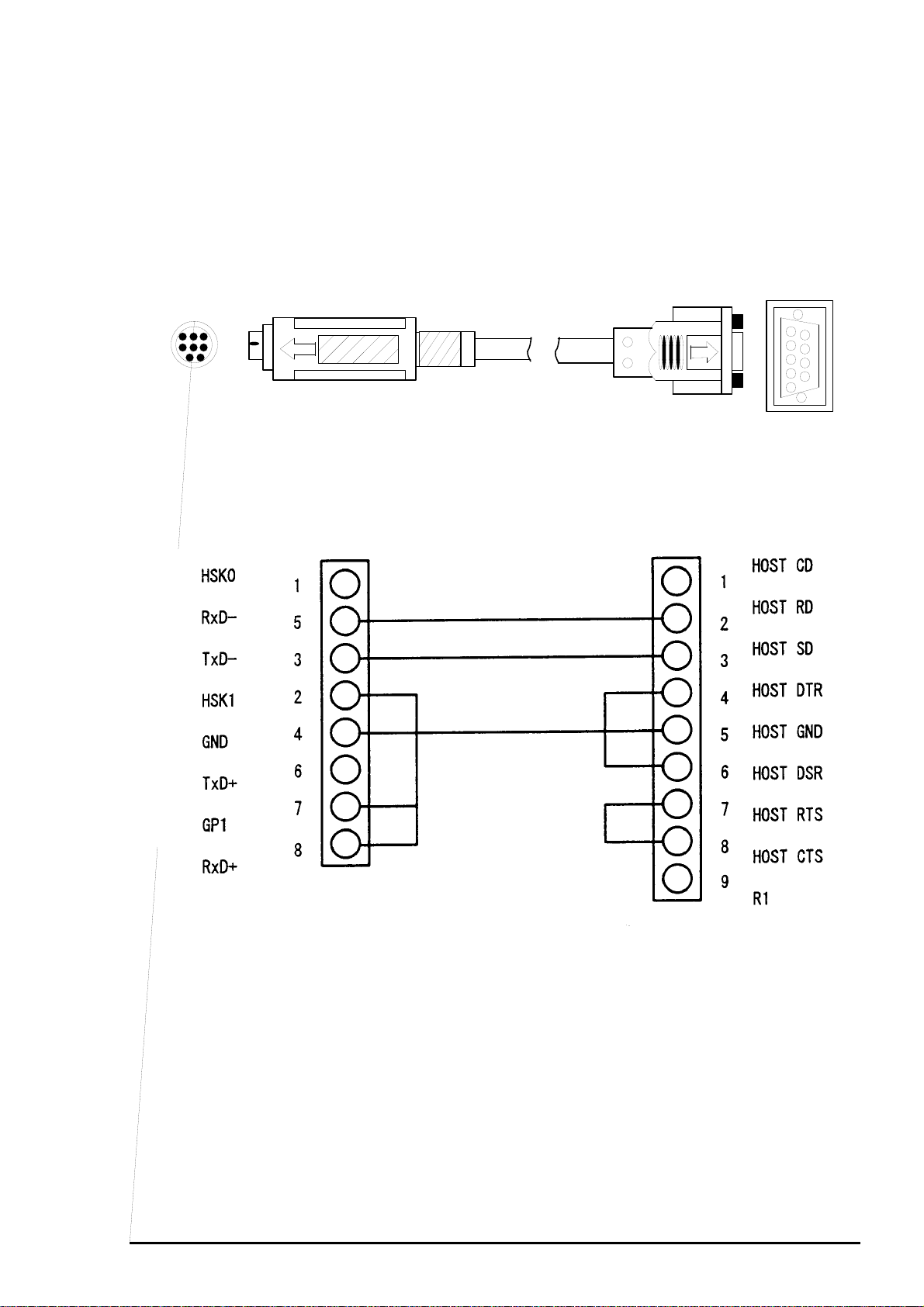
2.
The camera operation mode is displayed on the LCD. The following figure 1-7 shows its exterior and
its 8 displays.
Display A :
LCD Panel
Figure 1-7. LCD Panel
The number of pictures taken is indicated. If the camera is controlled by the PC,
the frame around the numbers flashes.
Display B :
S: Standard Resolution
Hi: High Resolution
Display C :
Display D:
Display E:
will flash and then turn off the power.
Display F:
Display G:
Display H:
communication with PC.
The present resolution type is indicated.
Erase indicator. This indicator flashes while the camera is deleting a picture.
Self-timer indicator. Indicator will flash when selftimer enable.
Battery life indicator. This indicates the 7 battery levels. When empty, indicator
Flash mode. Auto/No red-eyes auto/Forced flash/ Off. Refer to the
following figure. (See figure 1-8.)
Number of pictures remaining. This depends on the resolution setting you have chosen.
Connecting to PC. Line around the number of pictures taken will flash under
Line under the number of pictures taken will appear when cable is connected to
PhotoPC 500.
Rev. A
Page 16
PHOTOPC 500 SERVICE MANUAL Service Manual
0
Auto
3.
PhotoPC 500 has two indicators located on beside viewfinder and one on the left side above
of lens. The followings describe the location of indicators and description of these indicators.
LED Indicator
No red-eyes auto
Figure 1-8. Flash mode
Forced flash
Off
Figure 1-9. LED indicator
Indicator A:
*Red LED Red flashing: Photo shooting not available under following
conditions;
Image Processing/ Changing Flash/ Processing after Power ON
Red light : Full memory
Indicator B:
*
Stand -by Green LED Green light : Photo shooting available
Indicator C:
*Selftimer LED (red) After you set the self-timer;
0-7sec. light7-10 sec.flashing10 sec. Photo shooting
1
Rev. A
Page 17
Chapter 1 Product Description
4.
[Type]
Buttons on the LCD monitor
Size/LCD 1.8» TFT Color LCD
Of Pixels 61,000pixels H279 x V220
Power/Mode switch
Figure 1-10. Exterior view of LCD monitor
+ button
- button
MACRO button
MULTI button
[View (Recording) Mode]
[Playback Mode]
Monitor Display image from CCD in real time, display ratio: 1/30 sec.
Freezing image during processing
Brightness Adjustable with ‘+,-’ switch in only VIEW mode
Display level of brightness in adjustment (disappear in 3 sec.)
On-Screen Display Brightness level in VIEW mode
Macro mode
Close-up Function Macro switch (from 0.45cm)
Other If switch is set to VIEW mode under Power OFF, display warning message
in 10 sec. and then LCD power goes to OFF.
Playback Display Default: Full screen display for last picture
Selectable with ‘+,-’
On-Screen Display Image Number (disappear in 10 sec.)
Rev. A
11
Page 18

PHOTOPC 500 SERVICE MANUAL Service Manual
No image icon
[ERASE]
* After erasing, image number will be renumbered.
Slide Show 4sec./image
Start slide show by keep pushing ‘+’
Recycling all images
(Power save will be effective after one cycle of slide show)
Multi-Screen Multi-Screen in playback mode 9 image on screen using
thumbnail data
Other When PLAYBACK mode, control panel shows «LCD».
Even if camera’s Power switch is OFF, the camera can go to
PLAYBACK mode.
When LCD monitor is;
OFF : Erase last image by pushing Erase button
VIEW mode : Erase last image by pushing Erase button
PLAYBACK mode : Erase displayed image by pushing Erase button
(e.g. if #10 image erased, #11 will become #10 image)
[When connecting to PC]
[Button on LCD monitor]
5.
PhotoPC 500 has 2 methods in order to set or change the various functions ; either by the method
directly from the body or by using utility soft from the PC.
The following describes functions that can be set from the camera body or from the PC.
Power/mode switch OFF : LCD monitor power OFF
+button VIEW mode : Brightness control of LCD monitor
-button VIEW mode : Brightness control of LCD monitor
MACRO button Change mode alternately between MACRO recording mode
MULTI button Change mode alternately between 9 image display mode
Functional Setting
LCD monitor will be OFF, when connecting to PC.
(See figure1-10)
VIEW :VIEW mode
PLAYBACK :PLAYBACK mode
PLAYBACK mode: display next image
PLAYBACK mode: display previous image
and Normal recording mode.
This button is effective only VIEW mode.
Power ON default is Normal mode.
and Normal display mode.
This button is effective only PLAYBACK mode.
Power ON default is Normal mode.
[Available functions from the body]
[Available functions from the PC]
Resolution : Available either High Resolution or Standard Resolution
Flash : auto/forced flash/off by one button
Self-timer : On/Off
Shooting : Available
Power : On/Off
Erase one image : Erase for the last image
Erase all images : Erase button + Self timer button
Shutter speed : Available among Auto,1/30, 1/60, 1/125, 1/250, 1/1000.1/2000,
1/4000,1/10000 sec.
* In case of Auto, range will be set automatically from 1/30 to 1/10000.
12
Rev. A
Page 19

Chapter 1 Product Description
3
* When you down load the taken image data to the PC from the camera, the LCD on the camera indicate
« Low battery». Although this status appears even when the new batteries are installed, it is inevitable
phenomenon since it is done by voltage from battery detection.
Resolution : Available either High Resolution or Standard Resolution
Flash : auto/ forced flash/ off by one button
Self-timer : On/Off
Erase : Erase for the last image. Erase button + Self timer button erase all
images.
Date/Time : Set the same time as PC has. Available
year/month/date/time/second
setting.
Continuos image transfer
Communication speed 19200/38400/57600/115200 bps (This speed varies according to
the PC, O/S and application software.)
.6. Main Component
The followings are the main component of PhotoPC 500. Please refer to Chapter 2 for its location
and function.
1) SY1 Board 4) CA2 Board 7) Camera mechanism
2) CA1 Board 5) PW1 Board 8) TB2 Board
3) TB1 Board 6) ST1 Board 9) Housing
Rev. A
1
Page 20

HAPTER
C
2. O
PERATING PRINCIPLES
...............................................................................
..........................................................................................
............................................................................... 2.1.1.1. IC Function on CA1 Board2
..............................................................................................
......................................................................................................................2.1.3. Circuit Description11
.............................................................................................................2.1.4. PW1 Circuit Description12
..............................................................................................................2.1.5. SY1 Circuit Description13
............................................................................ 2.1.5.1. Internal Communication Bus14
.................................................................................................... 2.1.5.2. Power Supply Control14
..........................................................................................
............................................................................................. 2.1.6.1. Charging Circuit15
.................................................................................................... 2.1.6.2. Light Emission Circuit16
............................................................................................................
2.1. Operating Principles1
2.1.1. CA1 Circuit Description2
2.1.2. Outline of Operation11
2.1.6. ST1 Circuit Description15
2.1.7. LCD Block16
.1.
Page 21
.2. Operating Principles
This section desc ribes operation principle of c amera. Since the PhotoPC 500 is s till digital camera, there
is no complicated mechanism and most of the operation is done by the control of electric circuit. The
figure below explains location of each major electric circuit.
TB2 board
SY1 board
CA1 board
TB1 board
PW1 board
ST1 board
Figure 2- 1. PhotoPC 500 Board Location
Page 22
PhotoPC 500 Service Manual
1.
CA1 Circuit Description
The followings explain operating features on the CA1 board.
Independent storage and retrieval for each pixel
Square pixel unit cell
VGA compatible
R,G,B primary color mosaic filter
Continues variable speed electric shutter function
1.
IC Function on CA1 Board
IC903 (ICX084AK) CCD imager
IC902 (MC74HC04) H driver
IC904 (CXD1267AN) V driver
IC905 (CXA1690Q) CDS/AGC
IC906 (CXD2311AR) A/D converter
[1. IC903 (CCD)]
**Structure**
Interline type CCD image sensor
Optical size 1/3 inch
Effective pixels 659(H) x 494(V)
Pixels in total 692(H) x 504(V)
Chip size 5.84mm (H) x 4.94mm (V)
Unit cell size 7.4m(H) x 7.4 (V)
Optical black Horizontal (H) direction:
Front 2pixels, Rear 2pixels1
Vertical(V) direction:
Front 8pixels, Rear 2pixels
Dummy bit number Horizontal: 16
Vertical : 5
2
V
Pin 9
Pin 1
H
2
8
31
Figure 2- 3. Optional Black
Location
Note:
Photo sensor
Figure 2- 2. CCD Block Diagram
2
Rev. A
Page 23
3
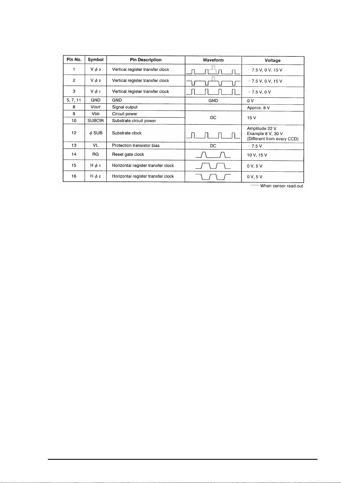
The following shows CCD Pin Description (IC903).
Chapter 2 Operating Principles
Figure 2- 4. IC903(CCD) Pin Description
Rev. A
Page 24
PhotoPC 500 Service Manual
4
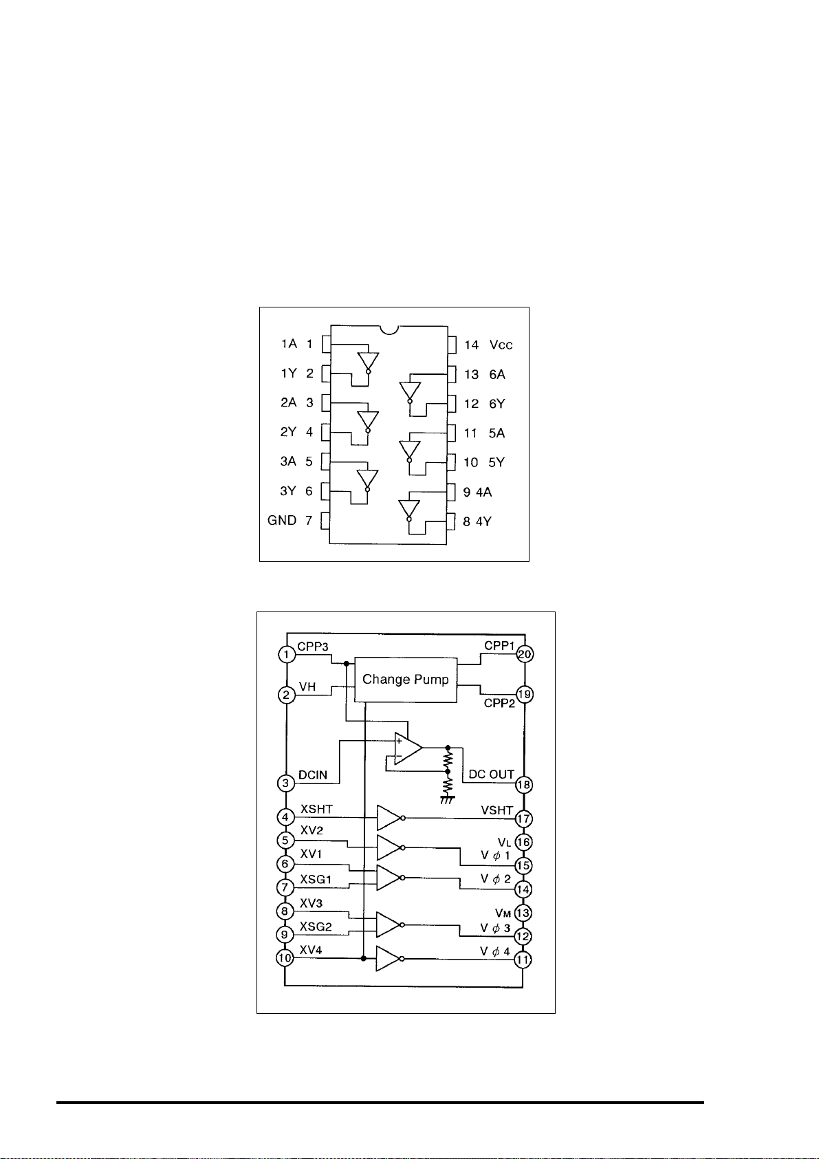
[2. H-Driver (IC902) and V-Driver (IC904)]
An H driver (IC902) and V driver (IC904) are necessary in order to generate the clocks (vertical transfer
clock, horizontal transfer clock and electronic shutter clock) which drive the CCD.
IC902 is an inverter IC which drives the horizontal CCDs(H1 and H2). In addition the XV1-XV3 signals
which are output from Pins(39)-(41) of IC102 on the CA2 circuit board are the vertical transfer clocks, and
the XSG signal which is output from Pin(43) of IC102 is superimposed onto XV2 and XV3 at IC904 in
order to generate a ternary pulse. In addition, the XSUB signal which is output from Pin(42) of IC102 is
used as the sweep pulse for the electronic shutter, and the RG signal which is output from Pin(38) of
IC102 is the reset gate clock.
Figure 2- 5. IC902 Block Diagram
Figure 2- 6. IC904 Block Diagram
Rev. A
Page 25
Chapter 2 Operating Principles
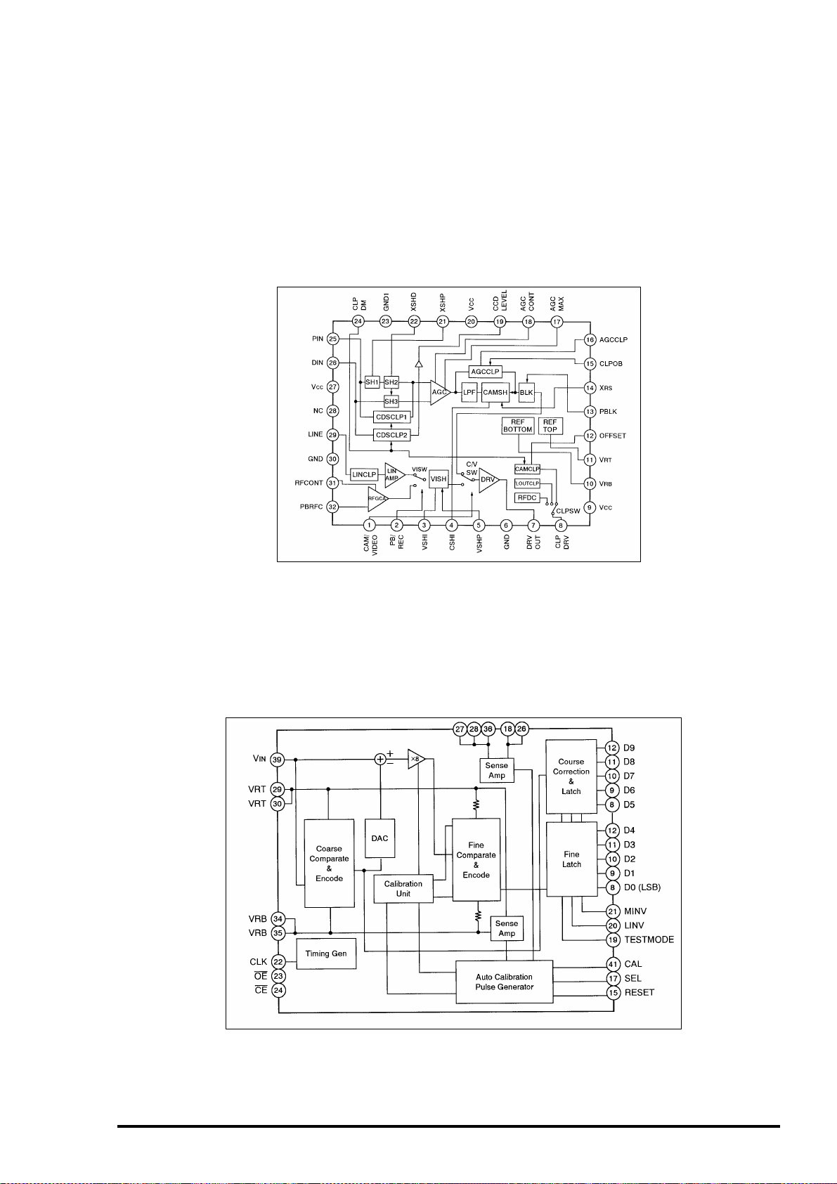
[3.IC905 (CDS/AGC Circuit)]
The video which is output from the CCD is input to Pins (25) and (26) of IC905. There are S/H blocks
inside IC905. There are S/H blocks inside IC905 generated from the XSHP and XSHD pulses, and it is
here that CDS (correlated double sampling) is carried out.
After passing through the CDS circuit, the signals pass through the AGC amplifier, LPF (low-pass
filter), S/H, blanking processing circuit, driver and clamper, after which they are sent to IC906.
The PWM voltage at Pin(18) is output from Pin(65) of IC102 and passes through the AND buffer of
IC907, after which it is smoothed, and this voltage controls the AGC amplifier gain.
Figure 2- 7. IC905 Block Diagram
[4. IC906 (A/D Converter)]
The video signal which is output from Pin(7) of IC905 and input to Pin(39) of IC906 is A/D-converted
to 10-bit signals inside this IC, and are then input to IC102.
A/D conversion is synchronized with the clock at Pin(22), and the reference voltages VRT(approximately
4.0V) and VRB(approximately 2.0V) are supplied from IC905.
Rev. A
Figure 2- 8. IC906 Block Diagram
5
Page 26
PhotoPC 500 Service Manual
6
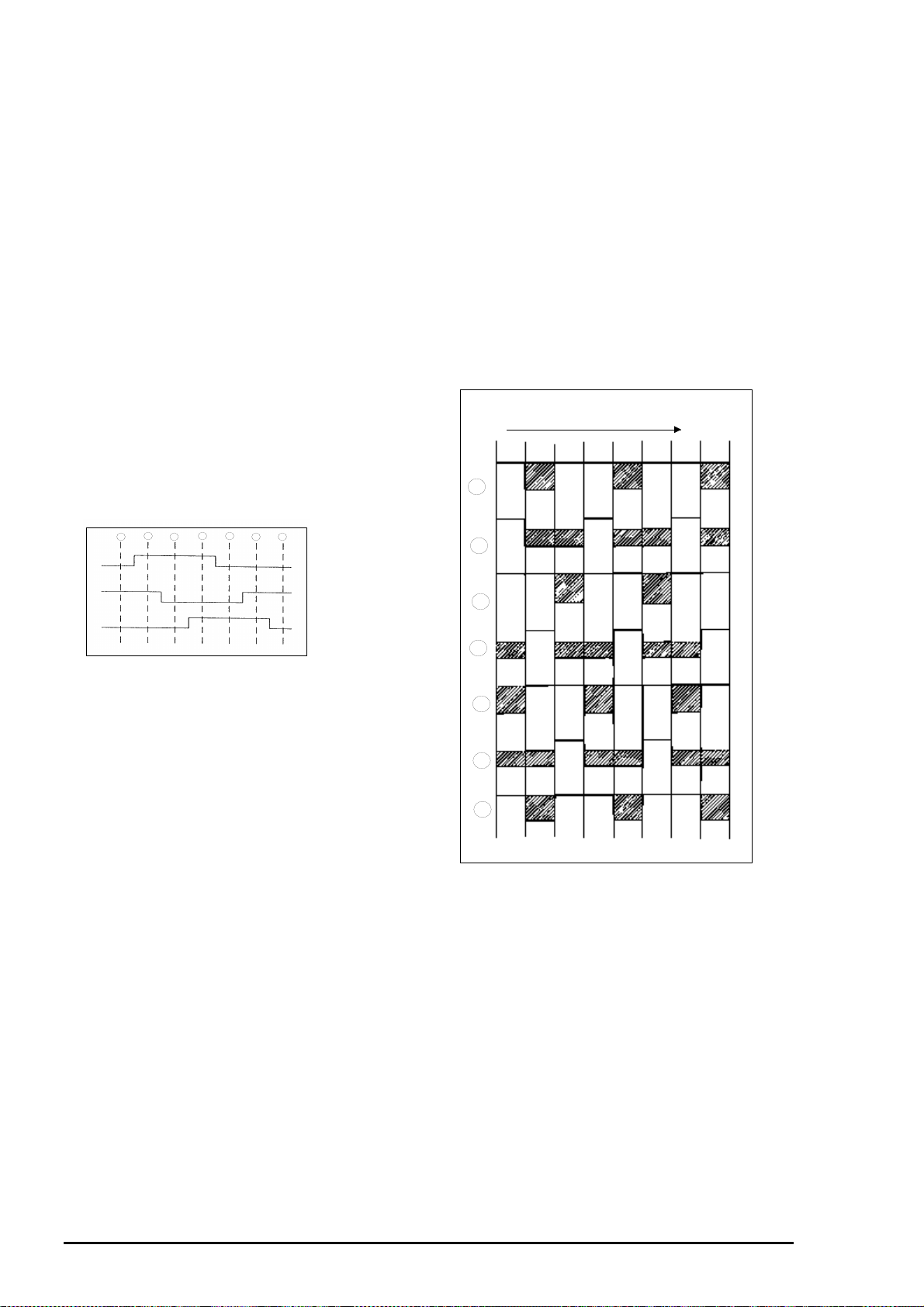
[5. Vertical Transfer Operation of the V Register]
The V register has three different electrodes which are designated as V1, V2 and V3. In step , the
potential at V2 is high and the potentials at V1 and 3 are low, so that there is a well at V2 for the
signal’s electric charge. In step , the potential at V1 becomes high, and so the well becomes wider
to include both V1 and V2. In step , the potential at V2 becomes low, causing the charge to accumulate
in the well at V1.The charge has thus been transferred by one electrode compared to the condition in
step . The condition at step represents a transfer of one pixel from the condition in step .
Direction of
transfer
V3 V2
1
V1
V3
V3
V2
V1V2
2
1
V1
V2
V3
4
3
5
6
7
Figure 2- 10. V1,V2 and V3
During the Horizontal Blanking
Period
2
3
4
5
6
7
Figure 2- 9. 3-Phase Drive Model Chart
Rev. A
Page 27
Chapter 2 Operating Principles
[6. V Register Read Operation from Photo Sensor]
This system employs the 3-value drive V register as shown in figure2-11.
During transfer of the V register, the applied voltage at the V register electrode is low. Therefore, the
electric charge for the signal cannot be output from the photo sensor section. However, since the
applied voltage during reading becomes high, the electric charge for the signal is transferred to the
V register.
Applied voltage
During transfer
During read
operation
V register(during transfer)
V3
V2
V1
V3
V2
V1
Direction of transfer
V register electrode
Light beam
Sensor electrode
Signal electric
charge
When reading P-Si
Photo sensor
section
During read
operation
A more detailed explanation is given below.
The transfer operation from the photo sensor
section to the V register is shown in Figure 2-12.
In Figure 2-12, V1 to V3 change as shown in
to . When V1(to V3) is -7.5V, the potential of the
V register becomes a barrier, and it becomes a
well when they are 0V. The potentials of V2 and
V3 and that of the sensor gate become the lowest
well under the condition at. Thus the signal
electric charges from the sensor section move to
V2 and V3 respectively, and are transferred as
shown in to.
Rev. A
Figure 2- 11. Read Out by 3-Value Drive
7
Page 28
PhotoPC 500 Service Manual
8
[7. Transfer of
Electric Charge by V
Register]
The H register sets H2
to a low potential
during H blanking, and
switches to a state of
waiting for a signal
from the V regis ter, as
shown in figure 2-13.
On the other hand,
during H blanking, the
V register
Light receiving section
V register
-7.5V
+15V
-7.5V
+15V
-7.5V
0V
0V
0V
which stopped during
the H scanning period
after switching V2 to
Figure 2- 12. Read Timing at the Sensor Section
low potential makes a
transfer
operation for one line based on 3-phase drive as shown by to in the figure.
Shaded section : Well
Other : Barrier
(Potential variations of H register during
the hrozontal blanking period.)
Figure 2- 13. Ve rtical Transfer of CCD and Application of Electric Charge
to the H Register
Because the H1 potential is lower than
the V2 potential, electric charges move
to H1 of the register.
Rev. A
Page 29
Chapter 2 Operating Principles
9
[8. Transfer of Electric Charge by the H Register]
The transfer system for the horizontal CCD employs a 2-phase drive method.
The electric charges sent to the final stage of the horizontal CCD are transferred to the floating
diffusion, as shown in figure 2-14. RG is turned on by the timing (1), and the floating diffusion is charged
to the potential of PD. The RG is turned off by the timing in (2). In this condition, the floating diffusion is
floated at high impedance.
The H1 potential becomes shallow by the timing in (3), and the electric charge now moves to the
floating diffusion.
Here, the electric charges are converted into voltages at the rate of V=Q/C by the equivalent capacitance
C. RG is then turned on again by the timing in (1) when the H1 potential becomes deep.
Thus, the potential of the floating diffusion charges in proportion to the quantity of transferred electric
charge, and becomes CCD output after being received by the source follower. The equivalent circuit
for the output circuit is shown in figure 2-15.
H1
H2
H2 H1
H1
H1
H1
H2
H1
H2
H2
H1
H1
H1
H2
HOG
HOG
HOG
RG
RG
RG
PD
PD
CCD OUT
CCD OUT
H1
H2
RG
CCD OUT
(1) (2) (3)
5V
0V
5V
0V
5V
0V
RG pulse leak signal
Signal voltage
Black level
Figure 2- 14. Horizontal Transfer of CCD Imager and Extraction of Signal Voltage
Rev. A
Page 30
PhotoPC 500 Service Manual
0
Reset gate
pulse
Direction of transfer
H Register
Electric
charge
Floating diffusion gate is
floated at a high impedance.
C is charged
equivalently
+B 15V Pre-charge
drain bias (PD)
Figure 2- 15. Theory of Signal Extraction
Operation
Voltage output
[9. Vertical Overflow Drain (VOFD)]
The CCD of this system is configured as shown in Figure 2-16. An imager which has OFD(SUB) provided
in the vertical direction(in the direction of depth) of a CCD chip is referred to as a CCD with a vertical
overflow drain (VOFD) construction. When the potential along the dotted line(A-A’) is seen from (a), it
appears as (b). The height of the potential barrier is decided by applying DC bias to the OFD from
outside.
This is the same as deterring the saturated electric amount Qs (equals the dynamic range) at the sensor.
Although a larger Qs is preferable, a Qs which is too large causes blooming (a phenomenon where the
electric charge becomes too large and leaks into other picture elements), which causes the picture
quality to deteriorate. Therefore, it is necessary to
V register
CS
A
ROG
Sensor
CS
apply a well-balanced DC bias.
[10. Electric Shutter]
During normal operations, read-out of the signal
charge can be made once for each field. Thus, the
storage time for the electric charge is 1/30 sec.
(a)
N-Si
A'
SUB(OFD)
However, the actual storage time can be shortened
by throwing away the electric charge during storage.
(Refer to figure2-17.) The electric shutter needs
this kind of electric charge throwaway operation.
The electric charge throw-away operation necessar y
for the electronic shutter in this system is controlled
V register
Sensor
SUB(OFD)
by the DC bias applied to the SUB.
Actually, the throwaway operation is done during the
horizontal blanking period in order to keep the
picture free from any noise that may appear. Under
(b)
Qs
VSUB=V1
normal conditions, the DC bias of the SUB is
overlapped by pulse. (Refer to figure2-18.)
In theory, it is possible to use the above system
to control an electric shutter with a storage time of
VSUB=V2
1/30 sec to 1/10000 sec, in units of 1/15750.
VSUB=V3
V1<V2<V3
Figure 2- 16. VOFD and Potential Chart
1
Rev. A
Page 31

Chapter 2 Operating Principles
Read-out pulse
Electronic
shutter control pulse
(electronic charge
throwaway pulse)
Read-out
1 field
Throwaway period
Throwaway
Actual
storage
time
Figure 2- 17. Theory of Electric shutter
operation
V(1/30 sec)
H
(1/15750 sec)
Storage time
(1/30 to1/10000 sec)
V(1/30 sec)
Storing time
(1/30 to1/10000)
Read-out
DC bias of OFD
Figure 2- 18. Actual Electric Shutter Control
2.
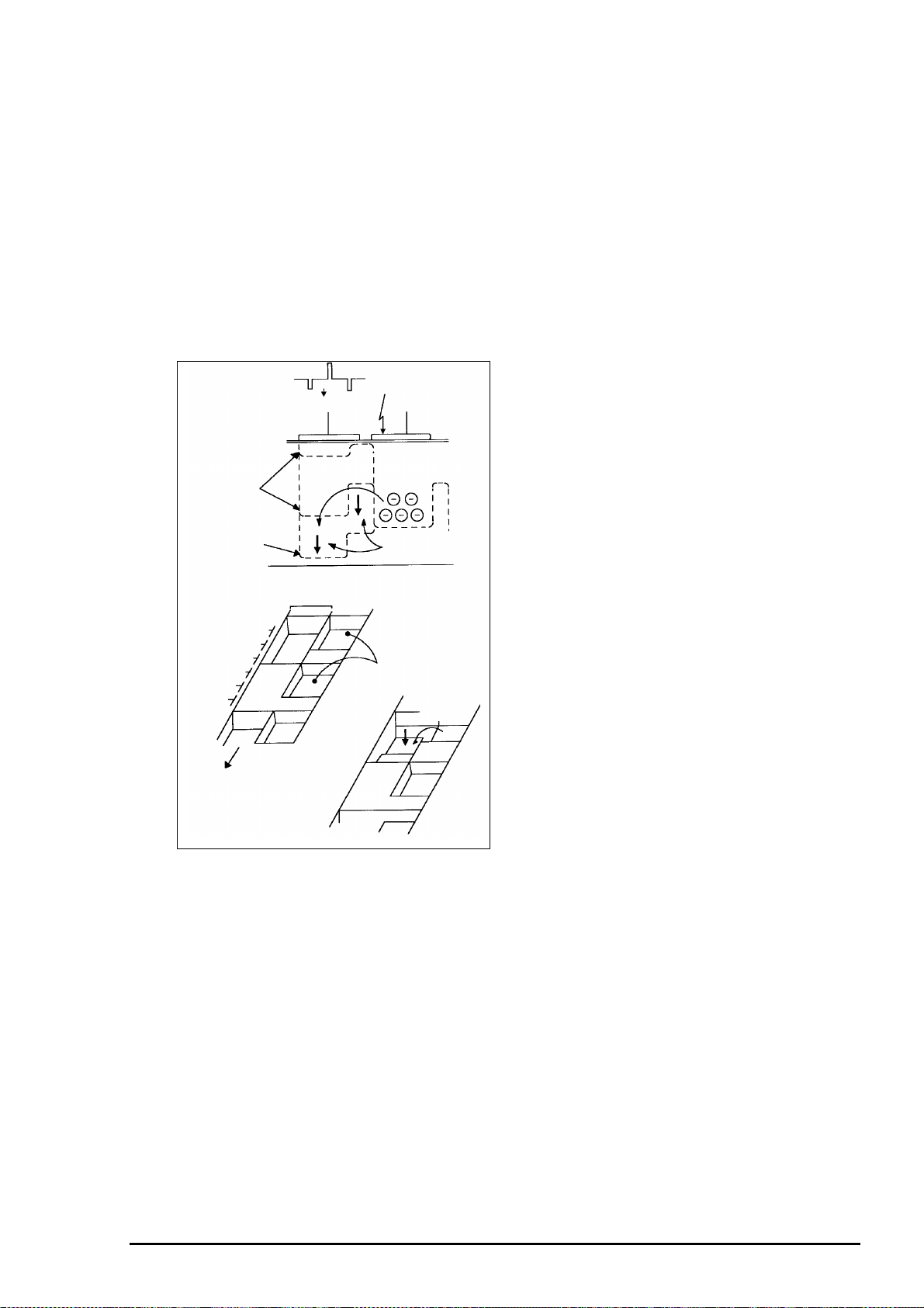
Outline of Operation
When the shutter opens, the reset signals (ASICand CPU) and the serial signals («take a picture»
commands) from the 4-bit microprocessor are input and operation starts. When the T G drives the CCD,
picture data passes through the A/D and is then input to the ASIC as 10- bit data. This data then passes
through the DCLP, AWB and circuits after which it is input to the DRAM. The AWB, shutter, and AGC
values are computed from this data, and three exposures are made to obtain the optimum picture.
The data which has already been stored in the DRAM is ready by the CPU and pixels interpolation is
carried out. Each pixel is interpolated from the surrounding data as being either R, G or B pr imary color
data to produce R, G and B data. At this time, cor rection of the lens distor tion which is a characteristic of
wide-angle lenses is carried out. The data is then compressed by the JPEG method and is then written to
flash memory.
When the data is to be output to an ex ternal device, it is read from the flash m emory and output via the
SIO.
3.
Circuit Description
1. Digital clamp circuit
The optical black section of the CCD extracts 16 pixel averaged values from the subsequent data to make
the black level of the CCD output data uniform for each line. The 16 pixel averaged value for each
line is taken as the sum of the value for the previous line multiplied by the coefficient k and the value f or
the the current line multiplied by the coefficient 1-k.
2. White balance circuit
The circuit controls the white balance by using the AWB judgment value computed by the CPU to
control the gain for each R, G and B pixel based on the CCD data which has been read.
3.circuit
This circuit performs (gamma) correction in order to maintain a linear relationship between the light
input to the camera and the light output from the picture screen.
Rev. A
11
Page 32

PhotoPC 500 Service Manual
4. 8-16 converter
This combines two clock sections of the 8-bit data which is output from the circuit and outputs
the resulting signal as 16-bit data.
5. DRAM controller
This circuit outputs address, RAS, CAS and AS data for controlling the DRAM. It also refreshes the
DRAM.
6.SIO
This circuit is used to send serial data to a personal computer. It conforms to RS-232C standards.
7.PIO
This is the interface for the 4-bit microprocessor.
8. TG block
This is the timing generation circuit which generates the clocks(vertical transfer clock, horizontal
transfer clock and electronic shutter clock) which drive the CCD.
4.
This is the main power circuit, and is comprised of the following blocks.
The followings explains the three major circuits.
1. Switching Controller (IC311,IC312)
This is the basic circuit which is necessary for controlling the power supply for a PWM-type switching
regulator, and is provided with two built-in channels. Feedback from both 5V(D) and 5V(A) power
supply outputs is received, and the PWM duty is varied so that each one is maintained at the correct
voltage setting level.
is recontrolled to restore output.
PW1 Circuit Description
Switching controller (IC311, IC312)
Digital system power output (T3101,Q3101)
Analog system power supply (T3102,Q3102)
Timer latch method short-circuit protection circuit
If output is short-circuited for the length of time determined by the condenser which is connected
to IC311 and Pin (2j) of IC312, all output is turned off. The control signal (P ON, P(A) ON)
Mis-operation prevention circuit for cases of low input voltage
Because there is a chance of mis-operation of the switching controller occurring under the
transit conditions which occur when the power is turned on and when there is a voltage
drop in the IC311 and IC312 power supply line, the power supply voltage level is monitored.
2. Digital System Power Output
5V(D) is output. Feedback is provided to the switching controller (IC311) so that PWM control can be
carried out.
3. Analog System Power Output
12
Rev. A
Page 33

Chapter 2 Operating Principles
3
5V (A),15V(A) and -7.5 V are output. Feedback for the 5V(A) line is provided to the switching controller
(IC312) so that PWM control can be carried out.
4. Output Control
The table below shows the relationship between both control signals (P ON, P(A) ON) and output.
Table 2-1. Control signal and output
Control Output
P-ON P(A)ON Digital Analog
5V(D) 5V(A) 15V(A) -7.5V(A)
L L OFF OFF OFF OFF
L H OFFONONON
H L ON OFF OFF OFF
H H ON ON ON ON
5. Specification
The following shows output at the Preview mode.
Table 2-2. Output at the Preview mode
5V(D) 5V(A) 15V(A) -7.5V(A)
Voltage
Electric current [mA]
5.
For the overall configuration of the SY1 circuit board, refer to the block diagram.
The configuration of the SY1 circuit board centers around a 4-bit microprocessor (IC301).
The 4-bit microprocessor handles the following functions.
1. Operation key input
2. Mode LCD display
3. Clock control and backups
4. Power ON/OFF
5. Strobe charge control
SY1 Circuit Description
Pin Signal I/O Outline
1 SCAN OUT3 O Key matrix output
2 /LCD ON O LCD monitor power ON/OFF signal L:ON
3 /P(A) ON O DC/DC converter(analog) ON\OFF signal L:ON
4 /P ON O DC/DC converter(digital) ON/OFF signal L:ON
5 /CHG ON O Flash charge ON/OFF signal L:ON
6 /ASIC TEST O ASIC reset control signal
7 /MAIN RESET O SPARC reset signal L:Reset output
8 ASIC RESET O ASIC reset signal L:Reset output
9 /STBY (R) LED O Standby LED (red) ON/OFF signal L:REset output
10 /STBY (G) LED O Standby LED (green) ON/OFF signal L:LED light
11 /SELF LED O Self-timer LED ON/OFF signal L:LED light
12 BUZ OUT O Buzzer output signal (4kHz)
13 /AD ON O AD converter power ON/OFF signal L:Test mode
14 RXD I RS-232C RXD input terminal
4.80 5.00 15.00 -7.50
380 108 9.7 2.8
Table 2-3. IC301 Pin functions
Rev. A
1
Page 34

PhotoPC 500 Service Manual
4
15 SCK O Serial clock output (ASIC)
16 SO O Serial data output (ASIC)
17 SI I Serial data input (ASIC)
18 /S. REQ I Serial communication request signal (ASIC) L:Serial request
19 DIN CONNECT I DIN jack connection detection signal H:SW ON
20 NOT USED -- --21 /RESET I Reset input
22 XIN I Main clock oscillation terminal (1 MHz)
23 XOUT O Main clock oscillation terminal
24 VSS --- GND
25 VDD --- VDD
26 XCOUT O Main clock oscillation terminal (32.768 MHz)
27 XCIN I Main clock oscillation terminal
28 AVSS --- Analog GND
29 VREF I Analog reference voltage input terminal
30 BATTERY I Battery voltage input (analog input)
31 CHG VOL I Strobe charge voltage input (analog input)
3233 S21-S20 O Mode LCD segment output
3437 SCAN IN 03 I Key matrix input
38 VLC3 I Mode LCD power input terminal
3940 S19S18 O Mode LCD segment output
41 NOT USED -- -4244 COM3-COM1 O Mode LCD common output
4561 S17-S1 O Mode LCD segment output
6264 SCAN OUT 02 O Key matrix output
1.
Internal Communication Bus
The SY1 circuit board carries out overall control of camera operation by detecting the input from the
keyboard and the condition of the camera circuits. The 4-bit microprocessor reads the signals from
each sensor element as input data and outputs this data to the camera circuits (ASIC) or to the
LCD display device as operation mode setting data.
Fig2-19 shows the internal communication between the 4-bit microprocessor, ASIC and SPARC lite
circuits.
Reset
S. REQ
4-bit
Microprocessor
ASIC SO
ASIC SI
ASIC SCK
ASIC
Data Bus
Reset
32-bit
SPARC
lite
Figure 2- 19. Internal Bus Communication System
2.
Power Supply Control
The 4-bit microprocessor controls the power supply for the entire system. The following is a description of
how the power supply is turned on and off.
When the battery is attached, a regulated 3.3V voltage is normally input to the 4-bit microprocessor
(IC301) by IC303, so that clock counting and key scanning is carried out even when the power switch
1
Rev. A
Page 35

Chapter 2 Operating Principles
is turned off, so that the camera can start up again.
When a switch is operated, the 4-bit microprocessor supplies power to the system as required. The 4bit microprocessor first sets both the /P(A) ON signal at pin (3) and the /P ON signal at pin (4) to Low,
and then turns on the DC/DC converter. After this, High signals are output from pins (7) and (8) so
that the ASIC and the SPARC lite are set to the active condition. If the LCD monitor is on, the /LCD
ON signal at pin (2) is set to Low, and the DC/DC converter for the LCD monitor is turned on.
Once SPARC lite processing is completed, the ASIC and the SPARC lite return to the reset condition,
all DC/DC converters are turned off and the power supply to the whole system is halted.
Table 2-4. Camera Mode (Battery Operation)
SPARC
Lite
Supply voltage 5V 5V 3.3V 5.0V 5V(A)
Power Power OFF OFF OFF OFF OFF OFF 32kHz OFF
OFFPlay backONONONONOFF1MHzON
Power SW ON
-
Auto power
down
Shutter SW ON ON ON ON ON ONOFF 1MHz OFF
SwitchONResolution,
Flash
Self timer SW
ON
LCD finder ON ON ON ON ON 1MHz ON
OFF OFF ON OFF OFF 1MHz OFF
OFF OFF ON OFF OFF 1MHz OFF
ASIC,
Memory
MODE
LCD
RS232C
Driver
CCD 4-bit
7.5V-15V
LCD
CPU
3.3V 11V4.8V
Monitor
-18V etc.
Table 2-5. Host Mode (Battery Operation)
SPARC
Lite
Supply voltage 5.0V 5.0V 3.3V 5.0V 5.V(A)
Power switch OFF OFF OFF OFF OFF OFF 32KHz OFF
Power SW ON-
Auto power down
Power Take a picture ON ON ON ON ONOFF 1MHz OFF
Switch Erase image ON ON ON ON OFF 1MHz OFF
ON Download image ON ON ON ON OFF 1MHz OFF
Continuous image ON ON ON ON ON 1MHx OFF
Message from
host
6.
1.
When UNREG power is supplied to the charge circuit and the CHG ON signal becomes High(3.3V),
the charging circuit starts operating and the main electrolytic capacitor is charged with high- voltage
direct current.
However, when the CHG ON signal is Low(0V), the charging circuit does not operate.
ST1 Circuit Description
Charging Circuit
OFF OFF ON OFF OFF 1MHz OFF
ON ON ON ON ON 1MHz OFF
ASIC.
Memory
MODE
LCD
RS232C
Driver
CCD 4-bit
7.5V-15V
LCD
CPU
3.3V 11V 4,8V
Monitor
-18V etc.
Rev. A
15
Page 36

PhotoPC 500 Service Manual
6
Power supply filter
L5401, L5402, C5401 and C5403 constitute the power supply filter. They smooth out ripples
in the current which accompany the switching of the oscillation transformer.
Oscillation control circuit
This circuit generates an AC voltage (pulse) in order to increase the UNREG power supply
voltage when drops in current occur. This circuit generates a drive pulse with a frequency of
approximately 15 kHz and shortens the pulse width in accordance with the state of the input
power supply in order to control the power consumption.
Oscillation transformer
The low-voltage alternating current which is generated by the conversion control circuit is
converted to a high-voltage alternating current by the oscillation transformer.
Rectifier circuit
The high-voltage alternating current which is generated at the secondary side of T5401
is rectified to produce a high voltage direct current and is accumulated at electrolytic capacitor
C5412 on the main circuit board.
Voltage monitoring circuit
This circuit is used to maintain the voltage accumulated at C5412 at a constant level.
After the charging voltage is divided and converted to a lower voltage by R5417, R5419 and
VR542, it is output to the SY1 circuit board as the monitoring voltage VMONIT.
When this VMONIT voltage reaches a specified level at the SY1 circuit board, the CHG
signal is switched to Low and charging is interrupted.
2.
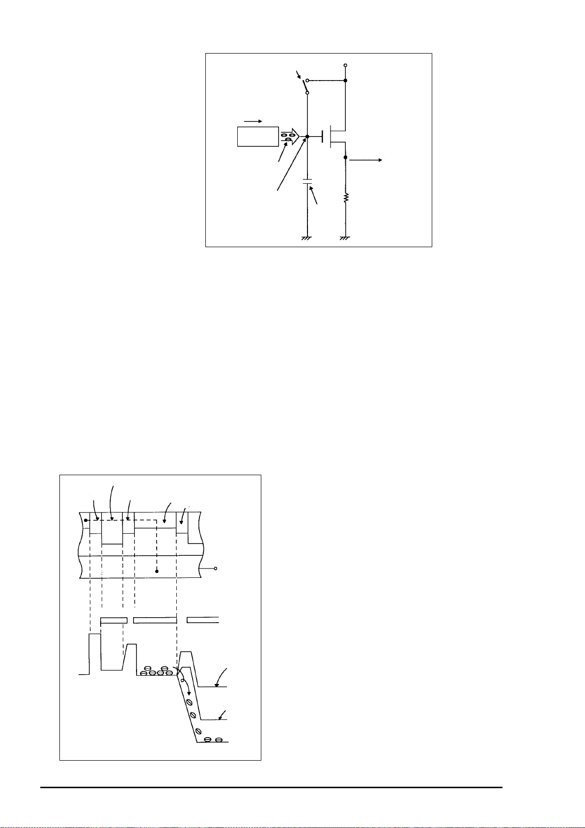
When RDY and TRIG signals are input from the ASIC expansion port, the stroboscope emits light.
stroboscope emits light.
7.
During EE, gamma compensation is carried out for the 10-bit RGB data which is input from the A/D
conversion block of the CCD to the ASIC in order that the RGB data can be displayed on the LCD.
Light Emission Circuit
Emission control circuit
When the RDY signal is input to the emission control circuit, Q5409 switches on and
preparation is made to let current flow to the light emitting element. Moreover, when a STOP
signal is input, the stroboscope stops emitting light.
Trigger circuit
When a TRIG signal is input to the trigger circuit, D5405 switches on, a high-voltage
pulse of several kilovolts is generated inside the trigger circuit, and this pulse is then
applied to the light emitting part.
Light emitting element
When the high-voltage pulse from the trigger circuit is applied to the light emitting part,
current flows to the light emitting element and light is emitted.
LCD Block
1
Rev. A
Page 37

Chapter 2 Operating Principles
The data is converted to 6-bit data at the LCD resolution of 279 x 220 pixels, and is then transferred
to the VRAM. The data which has accumulated in the VRAM is synchronized with the serial clock and
is then sent from the serial port to the ASIC. After D/A conversion is carried out inside the ASIC, the data
is sent to the LCD panel and displayed.
If the shutter button is pressed in this condition, the 10-bit data which is output from the A/D conversion
block of the CCD is sent to the DRAM (DMA transfer) as well as to the VRAM, and is displayed on
the LCD as a freeze-frame image.
During playback, the JPEG image data which has accumulated in the flash memory is converted to
RGB signals, after which it is converted to 6-bit data at the LCD resolution of 279 x 220 pixels.
In the same way as for EE, the data is then sent to the VRAM, after which D/A conversion is carried out
inside the ASIC, and then the data is sent to the LCD panel and displayed.
The LCD panel operates according to seven control signals and four analog signals from the ASIC,
and four power supply signals from PW2.
Of these, the four analog signals from the ASIC (VCOM, R, G, and B) are D/A output with small
amplitudes,
so that they are amplified by an external analog circuit to the amplitudes which are necessary for driving
the LCD panel. Because these analog signals do not include D and C components for the LCD elements
they are transformed at 1H intervals.
Because of the structure of the LCD, the VCOM is applied at a timing which is 1H delayed from the
timing actually measured. Because the LCD elements close more as the difference in potential
between the VCOM signal and the R, G and B signals becomes greater, the display becomes darker;
if the potential difference is smaller, the elements open and the screen becomes lighter. Furthermore, if
the D and C relationships between the VCOM signal and the R, G and B signals become displaced, it will
cause flickering in the LCD, so that adjustment will be necessary.
The D and C levels of VCOM adjust VR323 on the PW2 board in the LCD monitor unit.
Rev. A
17
Page 38

HAPTER
C
3. D
ISASSEBLY AND ASSEMBLY
............................................................................................
..........................................................................................................
.............................................................................................................................................3.1.2. Tools 1
............................................................................................................3.1.3. Specification for Screws 2
..........................................................................................
.................................................................................................................. 3.3. Assembly 7
.......................................................................................
..........................................................................3.3.2. Installing the Holder Chassis and TB1 Board 8
..........................3.3.3. Installing the TB2 Holder with TB2 Board, SY1 Board and Cabinet Top 9
...................................................3.3.4. Installing the PW1, ST1 Board, Lens VF and Reflector Unit 10
...........................................................................................................3.3.5. Installing the Lens Cover 12
.................................................................................... 3.3.6. Installing the Front and Back Cabinets 14
.....................................................................................................3.3.7. Assembling the LCD Monitor 16
................................................................................................................................
3.3.1. Setting up the CA1 Board 7
3.1. OVERVIEW 1
3.1.1. Precautions 1
3.2. Disassembly 3
.1.
Page 39

.2. OVERVIEW
This section describes various points to note when disassembling and assembling the camera.
There are two ways of maintenance; first maintenance and second maintenance. The performance
of the second maintenance is allowed to be done only by EPSON Co.,Ltd. The distinction between
first and second maintenance should be referred to Appendix (A-9, A-10 and A-11). Also, since
the assembly is more complicated than disassembly, refer to the section 3.3 when you actually
start assembling after disassembly.
1.
Follow the precautions below for disassembly and assembly.
Precautions
WARNING
There is a danger to get electric shock from the electrolytic condenser for flash. So, make sure
to refer to the section 3.2 (Step 2) and discharge the electric charge when you disassemble or
assemble ST1 board.
Remove all batteries before you start assembly and disassembly.
CAUTION
All the electronic parts on the CA1 board must not be r emoved. (Exc hange and r epair works for
all the electronic parts around the CA1 are allowed to be done only by EPSON. CO.,Ltd.)
When transporting the camera, use the exclusive package material.
2.
Table 3-1 lists the tools recommended for disassembling, assembling or adjusting the camera.
Note)
Note)
Tools
Table 3-1. Recommended Tools
No. Name Purchasable Code
1 Adjustment Program ------2 Color viewer 103058400
3 Tweezers B641000100
4 Soldering iron B740200100
5 Radio cutting pliers B740400100
6 Precison Driver () ------7 WICK (Desoldering wire ) -------
Tool No.1No.3 are used only by EPSON Co.,Ltd.
WICK is much easier to use compared with Soldering Cleaner when you do soldering.
3.
Page 40

Specification for Screws
Figure 3-1 lists the abbreviation of screws and its use.
Abbreviation Part Name Shape
Pan Head
Type of head
Type of threaded
section
Diameter
Length(L)
Configuration (Color)
Biding Head
Abbreviation Part Name
L
Dimension
(mm)
(Black)
(Black)
(Black)
(Gold)
(Gold)
Figure 3-1. Screw Indentification
No symbol Machine Screw
Forming Tight
Forming Tight
Most of PhotoPC-500
parts are fixed by this screws.
Battery cover and spring are fixed
by this screw.
Knob of power switch is fixed by
this screw.
Small screw on the CA1 board
for mounting the lens.
Lens unit is fixed on the CA1 board
from the back by these 2 screws.
Shape
(For plastic)
(For metal)
Location
Also, PhotoPC 500 has 7 boards and each of them is in charge of the following function.
Table 3-2. Board names and their functions
No. Board names Functions
1 SY1 Board Controls user’s interface of camera body.
2 PW1 Board Generates Digital and Analog power.
3 CA1 Board CCD mounted board with lens units.
4 TB1 Board Junction board for serial I/F connector and
inlet for AC adapter.
5 ST1 Board Controls stroboscope board and contains big
capacity of electrolytic capacitor.
6 PW2 Board Power board in the LCD body.
7 LCD Unit Playback, View.
Page 41

.3. Disassembly
Before you start disassembly, read section 3.1.1 carefully. Follow the order for disassembly
as it is described in the figure 3-2 to figure 3-5. Screws not particularly described in the figures
are M2x5.
Note)
When you remove the camera body from the front and back case, the holder terminal should be
Cover Back
Connector
Cover Plug
Slide the cover terminal
up before you start disassembly.
Cover
opened.
Cover Battery
Figure 3-2. Removing the Front and Back cabinets
Page 42

WARNING
Electrolytic capacitor mounted on the ST1 is for flash. If it is charged for flash even once, it
keeps high volume of electricity no matter whether the flash is used or not. Because of this, if the
capacitor is charged even once befor e disassembly, discharge the electricity by the following way
in order to avoid electric shock . Also, it takes 2 or 3 days for the electric ity in the capacitor to be
completely discharged in case of natural discharge.
Remove the ST1 board holding its edge.There is a possibility of getting electric shock if you
touch the soldering parts or elements on the board surface. Follow the direction at the [Step 2] to
release the electricity.
[Step 1]
[Step 2]
board.
Remove the ST1 board from the CA1 board.(Refer to in the figure3-3)
Let the cement resisor which has at least 560/10W touch the 2 soldering parts of the
capacitor at the back of the
Cement resistor (No fixed direction )
1k 10W 20W)
560
Lens VF
From the back of ST1 board, make the electric
poles touch the soldering parts of 330V and 160
(C5412).
*After removing this screw,
remove the 2-pin connector
F
(brown)on the TB1 board, so
that ST1 board is to be removed
easier.
PW1 Board
Reflector Unit
Holder Terminal
*Slide the cover terminal
up before you start
disassembly.
ST1 Board
*Be careful for electric shock(Refer to "WARNING" above)
Page 43

CAUTION
Since lead wires are connected among boards for pr evention of electrostatic noise, disc onnect
these wires using soldering iron acc ording to your nec essity. The points for as sembly is written on
section 3.3.
It is prohibited to exchange or repair all individual parts on the PW1 board. In stead, PW 1 board
itself should be replaced.
Perform the initialization and 5100K AWB adjustment when the CA1 board or lens parts (lens
unit, optical filter, rubber damper or CCD sensor) is replaced. Also, perform the Flange back
adjustment if the lens unit is replaced.
Assemble the lens unit, optical filter and rubber damper and fix them on the CA1 board with 3
screws before you solder the CCD sensor to the CA1 board.
24 pin connector and lens parts are not included in the spare parts when the CA1 board is
replaced. Therefore, when you assemble these parts by soldering, make sure, Mount the lens
parts, thenConnect the 24pin connector.
Use the rubber gloves when you handle the CCD sensor and be c areful not to touc h the electric
poles directly. Also, pay attention not to get dust or dirt on the CCD.
Cabinet Top
ST1 Board
TB2 board can be
*
removed from the
TB2 holder just
by one screw.
Rubber Damper
Optical Filter
Lens Unit
*Be careful not to drop
the optical filter and
rubber dumper when
you remove the lens unit.
Figure 3-4. Removing the Lens unit, TB1 and SY1 boards
TB2 Holder
CCD Sensor
Floppy Spacer
Connector
Screw
(M2x4, Gold)
Two Screws
(M2x6, Gold)
24pin Connector
* Since this 24pin connector
for LCD monitor is fixed by
soldering, it is required to
use soldering iron when
you remove or re-attach it.
TB1 Board
Holder Chassis
Page 44

WARNING
Solder the FPC cable steadily and correctly on the shield plate of the PW2 board. There is a
possibility of damaging if the cable touches other parts.
Perform the LCD V-com adjustment if the PW2 board or LCD monitor is replaced and make sure
that no thin horizontal lines appear on the screen. (Refer to Chapter 4 for details)
At repairing the LCD, the screen often gets greasy from hands. Using the scoch tapes can easily
clean this dirt. Never use the dry cloth for cleaning. Using the dry cloth for the LCD may cause
damage to the LCD because of static electricity.
FPC
FPC
PW2 Board
Figure 3-5. Removing the LCD monitor
LCD Monitor
Connector
Page 45

.4. Assembly
Since the PhotoPC 500 has rather complicated assembly than disassembly process, disassembly and
assembly process are separated and explained individually.
If you find unclear procedure during service, select the appropriate subject and refer to it.
1.
Setting up the CA1 Board
The CA1 board as spare parts does not include the lens related parts and 24 pin connector. Therefore,
this section describes how to assemble these parts.
CAUTION
Use the rubber gloves when you handle the CCD and never touch the CCD with your bare
hands. (Especially, never touch the electric poles)
If the lens related parts on the CA1 board, such as CA1 board itself or the CCD are replaced, it
is required to perform the initialization and 5,100K AWB adjustment. In this case, make sure to
complete these adjustment referring to the Chapter 4.
Insert the optical filter to the inside of the lens unit(crystal blue crystal sandwitch lens), pay ing
attention to the direction of the filter. ( The thinner crystal side should be the lens side) If the
direction is mistaken, the quality of image decreases.
Pick the both sides of optical filter by tweezers when you insert the filter to the inside of the lens
unit. Never touch the surface. If the surface of the filter is dirty, clean it with soft cloth and blow the
dust by the air-gun.
The rubber damper has a determined direction. But if you match the damper to the interior
shape of the lens unit holder, the direction matches automatically and it can be assembled easily.
[Step 1]
Assemble the lens unit as following in the figure 3-6 and fix them with 3 screws form the
back side of the CA1 board. The tightening torque for these screws are 2.5Kg.
Connect the 24-pin connector
to the CN110 on the CA1board
and solder the connector from
the side B of the board.
Optical filter
Lens unit
Floppy spacer
CCD sensor
Rubber damper
24-pin
CN.
(Back side of CA1board)
Fix with 3 screws(Gold)
2(M2x6), 1(M2x4)
Soldering the cable
Shield board
Small screw(M2x4)
Cable (Brown)
Figure 3-6. Installing the Lens unit
Page 46

[Step 2]
[Step 3]
Note)
If you find any dirt, clean it with soft cloth and blow the surface by the air-gun.
Solder all 16 points on the CCD sensor from the back of the CA1 board.
Solder the root of a small screw(M2x4: gold) out of three and a part of shield plate by the
brown cable.
After mounting the lens unit on the CA1 board, blow the surface of lens by the air-gun.
2.
[Step 4]
[Step 5]
[Step 6]
Installing the Holder Chassis and TB1 Board
Attach the TB1 board to the back of Holder chassis and fix them with two screws.
Attach the parts that are assembled at [Step 4] to the CA1 board and fix them with 3screws
from reversed side of the CA1 board.(side B) At this time, connect the connector of TB1
board to the CN105 on the CA1 board.
Attach the Holder terminal to the Holder chassis and fix them with 3 screws(2 screws for the
front and one for back).
Fix the Holder chassis
Install the
Holder terminal
Fix the TB1 board
Figure 3-7. Installing the Holder chassis and TB1 Holder
Page 47

3.
Installing the TB2 Holder with TB2 Board, SY1 Board
and Cabinet Top
[Step 7]
the CA1 board. Match 2 dimples on the CA1 board when you attach the TB2 Holder, so that
you can confirm the attaching points. At this time, Place the 2pin cable (brown) in the
holder hook as it is shown in the Figure below.
[Step 8]
top as it is shown in the figure below and push the Cabinet top into the holes on the SY1
board until it clicks.
Be careful not to remove the LCD board from the SY1 board by accident. Also, Do not
push the LCD board too hard in order to avoid damaging the crystalline liquid in the LCD.
If the LCD cover is removed, put the cover back after making sure that there is no finger
prints or dirt on the LCD surface.
[Step 9]
[Step 7] to the 2 connectors (CN106 and CN108) on the CA1 board.
[Step 10]
Attach the TB2 Holder to the CA1 Board and fix them with one screw from the back of
Insert the Cabinet top to the SY1 board. At this time, confirm the direction of the Cabinet
Connect the 2 connectors located at the bottom of the SY1 board, which is assembled at
Solder the shield plate coming out of SY1 board and top edge of shield plate on the
CA1 board .
Install the Cabinet top
and SY1 Board
*Push the Cabinet from
the right above.
Connect 2 connecters located
at the bottom of SY1 Board
to 2 connecters (CN106,
CN108) on the CA1 Board.
*Place the cable under
this hook.
Install the TB2 Board
Figure 3-8. Installing the TB Holder, SY1 Board and Cabinet
Fix by soldering.
Page 48

4.
Installing the PW1, ST1 Board, Lens VF and Reflector Unit
WARNING
Discharge the electricity in the electrolytic capacitor referring to Page 3-4, since there is a great
possibility of getting electric shock.
[Step 11]
[Step 12]
show in the figure below.
[Step 13]
of PW1 Board.
plate of CA1 Board.
Solder the one side of the cable(red) for electrosatic noise to the JW313 on the PW1 board.
Solder the other side of cable edge to the part of shield plate on the CA1 board, as it is
Solder the one side of the cable(white) to the shield plate on the PW1 board.
CA1 Shield Plate
Solder the cable (red) to JW313 on the side B
Solder the other side of cable on the shield
Figure 3-9. Soldering points for PW1 and SY1 boards.
JW313
(Side-B)
Back side of SY1 Board
Shield Plate on the CA1
Board
Solder the cable (white)to the
shield plate on side A of PW1 Board.
Solder the other side of cable to
the soldering at the back of SY1 board.
[Step 14]
[Step 15]
Note 1)
[Step 16]
Note 2)
At this time, fold the four cables for the flash control and put them together on the
Solder the other side of the cable(white) to the soldering side on the back of the SY1 board.
Connect the connector of the PW1 board to the CN104 on the CA1 board.
Place the 2-pin connector (brown) at the top edge of PW1 board.
Connect the ST1 board to the CN911 on the CA1 board.
electrolytic capacitor of the ST1 board.
Page 49

[Step 17]
Install the Lens VF in the Holder chassis and fix them with one screw. At this time, it is
easier to install this if you insert the Lens VF directly down to the Holder chassis.
In order to remove VF, pull it toward the camera front.
[Step 18]
[Step 19]
Install the reflector unit right side of Lens VF and fix it with one screw.
Connect the black and red cable(2pin, brown) coming out of TB2 holder to the brown
connector located between Holder chassis and ST1 board. At this time, make sure
that 4 cables(yellow, blue, red and white) coming out of reflector unit are located under the
black and red cable. (Refer to the figure below)
[Step 20]
Connect the black and red cable from the bottom of lens unit to the CN903 on the CA1
board.
*Be careful for electric shocks
(Refer to Page 3-4).
Figure 3-10. Installing the Lens VF and Reflector unit
Page 50

5.
Installing the Lens Cover
[Step 21]
[Step 22]
At this time, leave the lens cover closed.
[Step 23]
bottom of the right side ring and then insert the bottom peaking of lever lens to the notch of
cover lens. At this time, leave the lens cover still closed.
[Step 24]
of knob power on the front cabinet.
[Step 25]
from [Step 21] to [Step22], and fix them temporarily with 4 screws according to the
order in the figure below. Then tighten these 4 screws tightly at the same order shown
At this time, tighten screws holding the case by the one hand since the lens cover floats
[Step 26]
Note)
Place the ring along with the lens hole located back of the front cabinet.
Fit the hole of cover lens to the second protruding portion counting from right bottom of ring.
Paying attention for the direction, fit the hole of lever lens to the protruding portion located
Hang the peaking of lever lens on the notch of knob power and insert the knob to the notch
Paying attention to the direction, place the holder lens on the parts you have assembled
in the figure.
if you do this procedure leaving the cover on the desk.
Place the black and red lead wires(2pin) coming out of the leaf switch so that the
protruding portion should be between the soldering parts of wires. (This is for prevention
of short-circuit) Then fix the leaf switch with one screw(M1.7x8).
Knob power should be ON since the lens cover can not be installed correctly if it is OFF.
Page 51

process should be following;
[Step 27]
Perform
ON/OFF, pushing
the knob power
switch from the
behind and confirm
that
knob
power switch is
operating correctly.
Install the ring.
Install the cover lens,
leaving the cover closed.
4
2
3
Install the lever lens.
(Insert the protruding portion located at
bottom of lever to the trench of the ring)
Install the knob power.
1
Fix the holder lens and front
cabinet with screws.(Screw them
according to this order)
Figure 3-1 1. Installing the Lens cover
WARNING
When
the Knob
power
switch is
ON : Leaf
switch is
OFF
(White
actuator of
Leaf SW is
up)
When
the Knob
power
switch is
OFF :
Leaf switch
is ON
(White
actuator of
Leaf SW is
down)
Even if you can
perform ON/OFF normally with knob power, if the leaf switch is installed opposite, the knob power
switch can not be really ON state, but in s tead, it becomes O N state when the k nob power is set OF F.
So, make sure that leaf switch is installed correctly.
[Step 28]
Hang the 2 lead wires coming out of leaf spring on the hooks of the holder lens as it is
shown in the figure below.
Page 52

Black
Red
Note:This is the figure when the knob
power is OFF. Set the knob power
OFF, since it is very hard to fix
the leaf switch if knob power is ON.
Figure 3-12. Placing the Lead wires
Leaf Switch
Protruding portion
should be between
soldering parts.
Hang the lead wires on
these hooks.
6.
[Step 29]
[Step 30]
Installing the Front and Back Cabinets
From behind of the front cabinet, Install the battery cabinet in the right side and fix
it with 2 screws.
Insert the tripod stand into the left side ditch of the reversed front cabinet. Although there
is no determined direction for the tripod, 2 holes of tripod stand and cabinet should match.
Do not fix the tripod with screws at this time yet.
Page 53

Install the Tripod stand.
Install the battery cover.
(Leave the cover closed)
Figure 3-13. Installing the Battery cover and T ripod stand
Install the battery cover
matching with dimples for
location.
Fix it with 2 screws.
[Step 31]
[Step 32]
Install the battery cover.
Assemble the camera body and front cabinet and fix them with 3 screws. Take the black
and red wires from leaf switch out of the cabinet. Lead these wires under the camera
body to the side B of CA1 board, then connect them to the CN303(2pin, white) on the
SY1 board. Fix the wires on the shield plate with the scoch tapes.
[Step 33]
Put the back cabinet on and fix them with 6 screws and also fix the tripod stand
with 2 screws.
[Step 34]
Install the back cover, cover and plug cover.
Page 54

Left side of VF
on the chassis frame
Connect the lead wires from
the leaf SW to the SY1 Board.
(Fix these wires with tape on
the shield plate of CA1 Board)
Attach the cover.
Attach the back cover.
Fix the back cabinet.
CA1Board right
bottom
Attach the plug cover.
Left side of tripod stand
on the chassis frame.
Fix the body and front cabinet with
3 screws.
Note:If the body does not fit to the
cabinet smoothly, 2 electric poles
on the TB2 board might be deformed.
Open the battery cover and check
inside.
Fix the Tripod stand with
2 screws.
Figure 3-14. Installing Covers
7.
WARNING
Assembling the LCD Monitor
Page 55

Re-solder the FPC on the shield plate steadily when you assemble.
Perform the LCD V-com adjustment if the LCD monitor or PW2 board is replaced.
If the LCD screen gets dirty during the repair, clean it with scoch tapes. Never use the dry c loth
since electrostatic noise may cause some damages.
[Step 1]
[Step 2]
Attach the LCD to the LCD back cabinet and fix them with 4 screws.
Note)
If LCD gets dirty by finger prints or grease, clean it with scoch tapes.
Connect the 3pin connector(white, black, purple) from the LCD to the CN325 on the
PW2 board.
[Step 3]
[Step 4]
Note)
Fix the LCD back holder and LCD back cabinet together with 2 screws.
Fix the PW2 board to the LCD back cabinet together with 3 screws.
At this time, insert the switch on the PW2 board to the notch of slide switch on the
LCD back cabinet.
[Step 5]
[Step 6]
[Step 7]
Connect the FPC coming out of the LCD back holder to the CN321 on the PW2 board.
Connect the FPC from the LCD to the CN322 on the PW2 board.
Solder the FPC coming out of the LCD back holder for electrostatic noise on the shield plate
of the PW2 board.
[Step 8]
Re-solder the FPC on the
shield plate of PW2 board.
(On the same spot)
Fix the LCD front
cabinet.
Put the LCD front cabinet on the parts you have assembled and fix it with one screw.
Fix the LCD to the LCD back
cabinet.
Connect the FPC from the LCD
to the CN322 on the PW2 board.
Connect the FPC from the LCD
back holder to the CN321 on
the PW2 board.
Fix the LCD back holder.
Connect the back light cable
from LCD to the CN325(3pin,white)
on the side B of the PW2 board.
Fix the PW2 board and LCD back cabinet.
(Insert the switch on the board to the
notch of slide switch on the front cabinet)
Figure 3-15. Assembling the LCD monitor.
Page 56

Page 57

HAPTER
C
4. A
DJUSTMENT
4. ADJUSTMENT..........................................................................1
4.1. Adjustment OverviewSecond Maintenance)................................................. 1
4.1.1. PhotoPC 500 Adjustment procedure.............................................................................2
4.1.1.1. Adjustment Lists by the Calibration Program ............................................................3
4.1.2. Setting up and Connection.............................................................................................. 4
4.1.3. Adjusting Specifications..................................................................................................6
4.1.3.1. 5V(D) Voltage Adjustment.........................................................................................6
4.1.3.2. 5V(A) Voltage Adjustment .........................................................................................7
4.1.3.3. 4.8 V Voltage Adjustment..........................................................................................8
4.1.3.4. INV Voltage Adjustment...........................................................................................10
4.1.3.5. Initialization (only after replacing the CCD).............................................................. 11
4.1.3.6. 5,100K AWB adjustment .........................................................................................12
4.1.3.7. Flange-back Adjustment.......................................................................................... 13
4.1.3.8. LCD Vcom Level Adjustment...................................................................................14
4.
Page 58

5.
ADJUSTMENT
1.
This section describes electric and mechanical adjustment. Following tables list the required tools and
section 4.1.2 describes system requirements.
Adjustment OverviewSecond Maintenance)
CAUTION
The adjustments described in this section have to be performed only by EPSON Co.,Ltd.
The adjustments in the other branches are not allowed to do so.
Table 5-1. Required Adjustment Tools
No Required Tool Code No.
J-1 Color Viewer 5,100K 103058400
J-2 Siemens star chart Included in the end of this manual
book.
J-3 Calibration Software Included with this manual book.
Table 5-2. Adjustment Equipment
No. Required Materials
1 Oscilloscope
2 Digital voltmeter
3 IBM® Compatible PC (See section 4.1.2 for required conditions)
4 AC adapter (In case of battery, new battery is recommended)
Page 59

PhotoPC 500 Service Manual
1.
The table below describes adjustment procedure and required conditions.
PhotoPC 500 Adjustment procedure
Table 5-3. Required Adjustment
No. Adjustment items Required conditions
1
2
4
5
6
7 Flange- back adjustment
8 LCD Vcom DC level adjustment Perform this when the LCD monitor or PW2
5V(D) voltage adjustment
5V(A) voltage adjustment
4.8V (D) voltage adjustment
INV voltage adjustment
Initialization
5,100K AWB adjustment
(Only after replacing the CCD or
lens)
Perform this adjustment when IC311 or
IC312 on the PW1 board is replaced.
(Adjust Volumes on the board)
Perform this adjustm ent in case of f ollowing
situations.
1) After replacing the elements on the
PW2 board .
2) After replacing the PW2 board itself.
3) After replacing the LCD monitor.
Perform initialization in case of following
situations. Also, make sure to perfor m AW B
adjustment at No6. after this initialization.
1) After replacing CCD.
2) After replacing CA1 board.
3) After replacing lens unit.
Adjust the focus point between CCD and
lens, after CCD or lens is replaced.
board is replaced.
CAUTION
Make sure to perform 5,100K AWB adjustment at No.6 if you perform initialization at No.5.
2
Rev. A
Page 60

Chapter 4 Adjustment
3
1.
Adjustment Lists by the Calibration Program
Followings describe adjustments with program and figure 4-1 illustrates outlines of each adjustment.
Initialization
5,100K AWB Adjustment
LCD Vcom Adjustment
Perform this adjustment when the
CA1 board,lens unit or CCDsensor is replaced. Make sure
to perform AWB adjustment after this.
Not used.
This indicates firmware version which
this calibration program posses.If the
necessity to change the firmware version
occur on the market, it will be noticed. In that
case, erase *.bin on the file once, and
copy new *.bin and push "Fimware" button.
If the CA1board, lens unit, or CCD-sensor is
replaced, this AWB adjustment should be done
after the initialization.This adjustment requires
the special tool called "Color-Viewer".
Although this is not used for
normal repairs, it is helpful
to change brightness or
contrast because of LCD's
worn-out life or etc.
This is for V-com adjustment. Make sure to set
the value as "-1"
before starting LCD-Vcom
adjsutment.
Set here as "Gray" when
you perform LCD-Vcom
adjustment. After this
adjustment, it is also
possible to check by other
patterns. Also, in case of
5V(D) or 5V(A) adjustment,
select "Monitor"and adjust
voltage.
Figure 5-1. Adjustment lists by program
CAUTION
Purpose or usage of these adjustments are als o described in the «redme. tx t» of the program
file.
It is not necessary to use Calibration program for 4.8V, INV and Flange-back adjustments.
Make sure to perform the 5,100K AWB adjustment after the initialization is done.
Other materials may be used instead of Siemens star chart for Flange-back adjustment.
Rev. A
Page 61

PhotoPC 500 Service Manual
4
2.
1.System Requirements:
2. Installing Calibration software:
[Step 1]
[Step 2]
[Step 3]
[Step 4]
[Step 5]
[Step 6]
Setting up and Connection
Windows 95®
IBM®-compatible PC with 486 or higher processor
CD-ROM drive
Serial port with standard RS-232C interface
8MB RAM
Hard disk drive with at least 15MB available
VGA or SVGA monitor with at least 256- color display
3.5-inch high-density diskette drive
SnapShot or other equivalent application software
Insert the Calibration software diskette into your diskette drive.
Click on «Start button» and go to «Program».
From the Program, click on «Explorer».
Click on 3,5 inch FD.
Double click on «setup».
Follow the instruction on the screen.
CAUTION
Make sure that the camera is connected to the computer with serial cable and also power O N, when
you start the calibration program.
Rev. A
Page 62

3.Connecting the Camera to the computer
Chapter 4 Adjustment
[Step 1]
[Step 2]
[Step 3]
[Step 4]
[Step 5]
[Step 6]
Turn off both camera and computer.
Open the cover terminal.
Line up the arrow on the cable connector with the notch on the camera’s serial port,
and insert the connector.
Insert the serial cable according to the serial port indicated on your software.
Line up the serial connector on the cable with one of the serial ports on your computer,
and insert the connector.
Turn on the camera and your computer system.
AC Adapter
Serial Cable
To COM1 or COM2 serial port
Figure 5-2. Connecting the Camera to the Computer
Rev. A
5
Page 63

PhotoPC 500 Service Manual
6
3.
This section describes all 8 adjustments as they are listed on the table 4-4.
1.
This adjustment is to adjust the output of 5V(D) which is generated on the PW1 board.
This adjustment is required when IC311 or IC312 is replaced. The following figure 4-3 shows its
connection.
Adjusting Specifications
5V(D) Voltage Adjustment
CAUTION
If the PW1 board is replaced as unit, it is not necessary to perform this adjus tment since it is
already done at the factory.
Perform 5V(A) voltage adjustment after you perform this adjustment. (Refer to the section
4.1.3.2)
The following table shows the list of measuring point and check value.
Table 5-4. 5V(D) Adjustment check points
[Step 1]
[Step 2]
[Step 3]
[Step 4]
Measuring Point Measuring Equipment Condition
C1404+
C1404 -
ADJ. Location ADJ./ Check Value
VR311(PW1 board) 4.80 0.05 VDC
Connect the camera and computer and turn on both of them.
Start the Calibration soft and click on the «DscCal22» in the «DSC Calibration».
Click on the arrow at the right side of the Test window, and click on the Monitor.
Adjust with VR311 to 4.80 0.05 VDC.
Digital voltmeter Power ON
Rev. A
Page 64

To CA1
Chapter 4 Adjustment
CA1 Board (Side A)
PW1 Board
(Side B)
Figure 5-3. Connection for 5V(D)
2.
This adjustment is to adjust the output of 5V(A) which is generated on the PW1 board.
This adjustment is reuqired when IC311 or IC312 is replaced. The following figure 4-4 shows its
connection.
5V(A) Voltage Adjustment
CAUTION
If the PW1 board is replaced as unit, it is not necessary to perform this adjus tment since it is
already done at the factory.
Perform 5V(D) voltage adjustment before you perform this adjustment. (Refer to 4.1.3.1)
The following table shows the list of measuring point and check value.
[Step 1]
[Step 2]
[Step 3]
Rev. A
Table 5-5. 5V(A) Adjustment check point
Measuring Point Measuring Equipment Condition
C1403+
C1403 -
ADJ. Location ADJ./ Check Value
VR312 (PW 1 board) 5.00 0.05 VDC
Connect the camera and computer and turn on both of them.
Start the Calibration soft and click on the «DscCal22» in the «DSC Calibration».
Click on the arrow at the right side of the Test window, and click on the Monitor.
Digital voltmeter Power ON
7
Page 65

PhotoPC 500 Service Manual
8
[Step 4]
Adjust with VR312 to 5.00 0.05 VDC.
CA1 Board (Side A)
PW1 Board
(Side B)
To CA1
Figure 5-4. Connection for 5V(A)
3.
This adjustment is to adjust the output of 4.8V which is generated on the PW2 board. This adjustment
is necessary to be done after repairing the PW2 board or replacing the PW2 board or LCD.
4.8 V Voltage Adjustment
CAUTION
Some photos should be taken before this 4.8V voltage adjustment.
Perform INV voltage adjustment after this adjustment. (Refer to 4.1.3.4)
The following table shows the list of measuring point and check value.
Table 5-6. 4.8V Adjustment check points
Measuring Point Measuring Equipment Condition
4.8V(GND) Digital voltmeter Power : POWER ON
Monitor : PLAYBACK
ADJ. Location ADJ./ Check Value
VR321 4.80 0.05 VDC
[Step 1]
Disassemble the LCD and remove the front and back cabinets. Connect the
Rev. A
Page 66

9
[Step 2]
[Step 3]
[Step 4]
Chapter 4 Adjustment
body which has no cabinets to the camera. At this time, wrap the metal part
located back side of the LCD with insulating tape.
Disconnect the shield plate in the side B of PW2 board by the soldering iron, and
touch the points with probes of the voltmeter as it is shown in the figure below.
Switch ON the camera and set the monitor unit switch «PLAYBACK».
Displaying taken data on the LCD, adjust with VR321 to 4.80 0.05 VDC.
PW2 Board (Side B)
Shield Plate
CN325
To Back light
GND
VR324
VR321
4.8V
VR323
1AG4B10B27700B
Figure 5-5. Connection for 4.8V
+
-
Rev. A
Page 67

PhotoPC 500 Service Manual
0
4.
This adjustment is to adjust the output of INV voltage which is generated on the PW2 board.
This adjustment is necessar y to be done after repairing the PW2 board or replac ing the PW2 board or
LCD.
INV Voltage Adjustment
CAUTION
Some photos should be taken before this INV voltage adjustment.
Perform 4.8V voltage adjustment before this adjustment. (Refer to 4.1.3.3)
The following table shows the list of measuring point and check value.
Table 5-7. INV Adjustment check points
Measuring Point Measuring Equipment Condition
INV(GND) Digital voltmeter Power : POWER ON
Monitor: PLAYBACK
ADJ. Location ADJ./ Check Value
VR322 6.20 0.05 VDC
CAUTION
If the code number on the PW2 board is silk-printed as «1AG410B27700B», INV would be misprinted
as 4.8V. Therefore, be careful and perform adjustment referring to the figure below. The boards that
the last alphabet is printed as «C» or after the «C» alphabets should be printed correctly as INV.
[Step 1]
[Step 2]
[Step 3]
[Step 4]
Disassemble the LCD and remove the front and back cabinets. Connect that
body which has no cabinets to the camera. At this time, wrap the metal part
located back side of the LCD with pressure sensitive adhesive tape or sheet for
insulating.
Disconnect the shield plate in the side B of PW2 board by the soldering gun, and
touch the points with probes of the voltmeter as it is shown in the figure below.
Switch ON the camera and set the monitor unit switch «PLAYBACK».
Displaying taken data on the LCD, adjust with VR322 to 6.20 0.05 VDC.
1
Rev. A
Page 68

PW2 Board (Side B)
Shield Plate
GND
Chapter 4 Adjustment
VR324
VR322
CN325
VR321
1AG4B10B27700B
To Back light
+
Figure 5-6. Connection for INV
5.
This operation is required when replacing the CCD or CA1 board since the values of electric
characteristics for the individual CCD are already adjusted at the factory and are stored in the Flash
memory. The following figure 4-7 shows its connection.
Initialization (only after replacing the CCD)
[Step 1]
[Step 2]
[Step 3]
[Step 4]
[Step 5]
[Step 6]
CAUTION
It is not necessary to perform this operation, if the CCD, CA1 board or lens unit is not replaced.
Make sure to perform 5,100K AWB adjustment after this operation. (Refer to 4.1.3.6)
Turn on the camera.
Double click on the «DscCal22».
Click the initialize and click the Yes.
After initialization is completed, a message «Initialize Camera :Complete» will appear
on the screen.
Click on OK.
Perform 5,100K AWB adjustment referring to 4.1.3.6.
Rev. A
11
Page 69

PhotoPC 500 Service Manual
Serial cable
Power
Camera
Figure 5-7. Adjusting location for initialization
6.
This adjustment makes the camera body receive the lights emitted from the color viewer and store the
values of white balance. Followings describe its connection.
5,100K AWB adjustment
CAUTION
When you perform this adjustment, be careful not to let any lights enter from outside.
Perform this adjustment after the initialization adjustment described at 4.1.3.5.
You may hold the camera when you want to locate the camera closer to the viewer.
[Step 1]
[Step 2]
[Step 3]
[Step 4]
12
Locate the camera closer to the color viewer approximately 23cm so that all white
Start the Calibration soft and click on the «DscCal22» in the «DSC Calibration».
Turn on the camera.
Follow next steps:1)Plug in the AC-adapter, 2)Set the VR of the color viewer to the
maximum towards right direction, 3)Turn on the SW on the VR, 4)Turn on the
switch on the main body of color viewer.
pattern becomes a full picture. (Do not enter any light)
Rev. A
Page 70

Chapter 4 Adjustment
3
CAUTION
This program reads emitted lights from the color v iewer three times and indicates their mean values
as R, G, B on the screen. At this time, pay attention to the following points. If these three values are
out of regulated range listed below, there is a high possibility of malfunction in the CCD or CA1 board.
Therefore, perform this adjustment after replacingthe CCD, CA1board, or lens unit and make sure
these three values are within the following range.
R :Should be within 300530.
G :Should be 128. Replace the CA1 board if the value is not 128.
B :Should be within 100200
[Step 5]
[Step 6]
[Step 7]
Click on AWB, and click on Yes.
AWB adjustment value will appear on the screen. (Check if each 3 values is within the
range or not)
Click on OK.
Serial cable
Approx.
2-3cm
Power
All white pattern
Camera
Figure 5-8. Adjusting location for 5,100K AWB
Color viewer (5,100K)
7.
This adjustm ent is required only when replacing or disassembling the CCD or lens unit in order to adjus t
focus. W ith a plus screw driver, this adjustment should be done by turning the adjustm ent screw either
clockwise or counter-clockwise. This screw can be seen from the notch of the back side of CA1 board.
Flange- back Adjustment
CAUTION
This adjustment is not necessary if the CCD or lens unit are not disassembled or replaced.
Since this adjustment is not required to use Calibration soft, Win3.1 can be used instead of
Win95.
For this adjustment, other materials can be used instead of using the Siemens star chart.
[Step 1]
[Step 2]
[Step 3]
[Step 4]
Rev. A
Click on the Photo PC or Scanner icon, and then click the «OK»
button in the For Your Information message box.
Click on Camera Options.
Click on «Show Live Preview» in the Controls window. The images captured
Double-click on the SnapShot icon (or equivalent application soft).
1
Page 71

PhotoPC 500 Service Manual
4
by the camera will appear in succession.
Turning screw clockwise : The focal length of the lens will decrease.
T urning screw counter-clockwise : The focal length will increase.
CAUTION
[Step 5]
[Step 6]
[Step 7]
[Step 8]
While keeping the distance from the lens the same, position the two Siemens
charts so that they can both be projected simultaneously.
Project two Siemens star charts at a distance of 1.0 meters and 0.15 meters
in front of the lens.
Turn the adjustment screw until the Siemens star which is 1.0 meters away is
exactly in focus. Check that the Siemens star which is 0.15 meters from the
front of the lens is out of focus at this time.
Apply thread locking agent to the area around the adjustment screw and nut.
CA1 Board
Lens
Location to apply
Adjustment
screw
Adjustment
screw
Screwdriver (+)
Figure 5-9. Adjusting location for Flange-back
8.
This adjustment should be done after the LCD or PW2 board is replaced or repaired. This performance
adjust the relative balance of V-com signal which is an abbreviation of Video-Composite signal and
LCD Vcom Level Adjustment
CAUTION
Green signal which represents the 3 values of RGB.
Take some photos before you perform this adjustment.
[Step 1]
[Step 2]
Note)
[Step 3]
1
Disassemble the LCD unit. (Remove the front and back cabinets.)
Solder the extended cables at the 3 soldering points (for Green, V-com and GND),
referring to the figure4-10 below.
Do not make the extended cables longer than necessary. About 10cm will be
adequate.
Since the PW2 board and metal part located back side of the LCD will be side by side,
Rev. A
Page 72

wrap this metal part with insulating tape.
Chapter 4 Adjustment
PW2 Board (Side B)
To Back light
[Step 4]
[Step 5]
Note)
[Step 6]
Note)
[Step 7]
[Step 8]
(Side A)
Shield Plate
Shield Plate
PW2 Board
GND
Soldering point
VR324
VR321
4.8V
for GND
Soldering point
Soldering point
for Green
for Vcom
CN325
1AG4B10B27700B
VR323
Figure 5-10. Soldering points for extended cables
Connect the LCD and PW2 board electrically, and connect them to the camera
and turn on the camera.
Start the Calibration program and set the value in the V-com window as «-1».
At this time, Gray pattern will appear inspite of the location of the switch on the PW2
board.
Since 2 channels of the oscilloscope are used, correspond the each GND level before
hands.
At this time, each video signals form rectangular wave towards minus, it is necessary
to set the GND relatively upward.
Connect the ch.1 of the oscilloscope to the Vcom, and connect the ch.2 to the Green.
Then fix the hooks of probe for GND at the soldering part for GND as it is shown
in the figure above.
Change the oscilloscope from the GND to DC, and set the volume level as 1V or 2V.
Rev. A
15
Page 73

PhotoPC 500 Service Manual
6
ch1: Vcom signal
(approx.6V[P-P])
ch2:Green signal
(approx.1V[P-P])
Figure 5-1 1. Waveform for LCD Vcom DC level adjustment
Green waveform
center value
Vcom waveform
center value
[Step 9]
[Step 10]
marks on the oscilloscope screen)
[Step 11]
than the green signal center value. Following figure shows completed wave forms
Following waveform should be seen on the oscilloscope screen.
Check the center values of Vcom and Green waveforms. ( Make a record or
Adjust VR323 the adjustment value until the Vcom center value becomes 1.5V lower
after this adjustment is done.
Figure 5-12. Completed waveform for LCD Vcom level adjustment
1
Rev. A
Page 74

HAPTER
C
ROUBLESHOOTING
5 T
........................................
...............................................................................5.2. Check points on the Waveform3
..........................................................................................................................................
..........................................................................................................................................
5.1. TROUBLE SHOOTING (SECOND MAINTENANCE)1
Page 75

Chapter 5 Troubleshooting
.1. TROUBLE SHOOTING (SECOND MAINTENANCE)
This section describes troubleshooting for typical 3 phenomena of camera malfunction. Refer to the
Check list on the page 5-25-8 if necessary and confirm the m ulfunction points. «Chec k» on the flowchart
means to check the driving wave form and signal voltage level.
YES
Press Shutter
button
IC301-36,37
(SCAN IN 2,3)
PULSE INPUT
CN302-6,7
(P ON, P(A) ON)
CN302-12
5V
IC301-6,7,8,
High
Serial
communication
Check CA1
NO CHECK 3029,
YES
Low
High
No
YES
No
YES
NG
OK
R3022, R3023,
D3015, D3016
Check IC301,Q3005,
Q3006, PW1
Check PW1
Check IC301 or
CA1
Check IC301,R3015,
R3032, Q3003,CA1
Error Code
On LCD
NO
CLK (48MHz)
input to
IC102-108(CLK IN)
OK
CLK (24MHz)
input to
IC101-115(XTAL1)
OK
IC102-148 (ZAS)
OK
IC101-90
(ZBREQ)
OK
IC102-146
(ZBGRNT)
OK
IC101-147,148
(IRL1,2)
OK
Check soldering of
each CPU,ASIC
and Memory pin.
Check each device according
to error codes on the
LCD panel.
NG
Main clock for system operation.
No operation if absent.
Check X1001 oscillator.
NG
Basic CPU block.
Check ASIC 82pin.
NG
Always appears when CPU,ETC is accessed.
Check if CPU is reading program, and
check address and data bus of IC132-IC133.
Request for use of data bus from
NG
ASIC to CPU.No DMA transmission
if absent. Check IC102-149
Receives ZBREQ signal and gives permission
NG
to ASIC for use of data bus. No DMA
transmission if absent.
Check IC101-94.
NG
Incorrect handshaking.
Between 4-bit CPU and
RS-232C.
Check each interface.
Figure 5-1. No Pictures
Figure 5-1.Taking Inoperative
ON
High
High
High
Yes
Yes
CLOSED
Yes
Low
Check power SW,
CN303,
R3020, D3014
Low
Low
Check IC303
No
No
No
BARRIER SW ON
Check
TB1, CA2
Check
IC304,R3051
Check X3001,
R3008,C3003,
C3004
Check X3002,
R3007,C3001,
C3002
BARRIER SW
IC301-34
(SCAN IN 0)
PULSE INPUT
IC303-2
(UNREG)
IC301-25
(VDD)
IC301-21
(RESET)
IC301-23
Oscillation
IC301-26
Oscillation
Normal
** Please refer to the next page for the error code.
Rev. A
Check IC301
Figure 5-2. Power Loss Inoperative
1
Page 76

PhotoPC 500 Service Manual
* Following list shows error codes on the LCD panel.
Table 5-1. Error codes
Error Code Contents
1,2 Error writing to image flash.
3 Flash file system is corrupted.
4 Chksum in image flash template is not empty. File system is corrupted.
5 T emplate data is not empty. Flash file sysytem is corrupted.
68 Flash file system is corrupted.
9 Error writing to image flash.
10 Error copying to flash file system.
12,13 Error writing to image flash.
14 Error copying to flash file system.
15 Means flash memory- not all erased or bad.
16 Bad flash bank detected.
17 No image flash ram detected/formatted.
18 Copy CAMDEF failed.
19,20 Error writing CAMDEF chksum to image flash.
21,22 Error writing to image flash.
23,24 Error writing CAMDEF chksum to image flash.
2528,30,31 Error writing to image flash.
3235 Error writing to image flash.
36 Flash file system is corrupted.
37,38 Error writing to image flash.
4049 4-bit micro/ASIC commerror.
50 Somehow PICFILEPTR must be bad. Flash file system is corrupted.
51 Out of DRAM memory.
52 Copy CAMDEF to image flash failed.
53 Too many reconstruct retries-give up.
54 Unable to erase NON-BOOT Block(S) of program flash mem.
5558 Disaster returns from updating program flash.
56 Invalid checksum on newly downloaded firmware.
57 Unable to write checksum for newly downloaded firmware.
58 Program Code is too long.
59 Download program is too long,or bad-no longer used.
60 Attempted to write to non-erased image flash.
61 More than one picture template is found. Image file system is corrupted.
99 Debug to catch infinite loop.
2
Rev. A
Page 77

Chapter 5 Troubleshooting
3
.2. Check points on the Waveform
This section describes various devices wave formats to check if they are working properly or not.
The following wave formats are at the normal state. Check the wave forms about
Figure 5-3. Waveform
parts you find from the flow chart on the Section 5.1. and perform proper repairs.
Rev. A
Page 78

PhotoPC 500 Service Manual
4
Rev. A
Page 79

HAPTER
C
6. MAINTENANCE........................................................................1
6.1. Preventive Maintenance..................................................................................1
6. M
AINTENANCE
Page 80

Chapter6 Maintenance
6.
1.
This PhotoPC 500 does not require specific maintenance on a regular basis or consumable items to
exchange. Therefore, perform cleaning when you repair or finish repairing according to its necessity .
MAINTENANCE
Preventive Maintenance
CAUTION
Do not use paint thinner, trichloroethyylene, or ketone-based solvents for cleaning. These
chemicals can damage or deform plastic components and rubber parts.
Do not use a hard or abrasive brush for cleaning.
Be careful not to damage components when cleaning inside of camera.
Rev. A
1
Page 81

PPENDIX
A
....................................................................................
...............................................................................................A.2. Leadless Component4
...................................................................................................
.....................................................................................................................A.2.2. Leadless Resistors7
............................................................................................................................ A.2.3. Leadless Coils8
..................................................................................................................... A.2.4. Leadless Tantalum8
..................................................................................
.....................................................
A.3.1. Circuit Diagrams and Board Component Layouts.13
A.1. ABBREVIATIONS 1
A.2.1. Leadless Diodes6
A.3. Exploded Diagram10
Page 82

.1.
Page 83

.2. ABBREVIATIONS
1. CA1 Board:
[A]
AD Analog-To-Digital
AD[0:9] Analog-To-Digital data
ADCK AD Clock
AGC Automatic Gain Control
[C]
[D]
[E]
[H]
[O]
[P]
[V]
CCD Change Coupled Device
CDS Correlated Double
CE Chip Enable
CLP Clamp Pulse
D[0:9] Data
DRV Drive
EF Emitter Follower
H DRIVE Horizontal Drive
OE Output Enable
O-LPF Optical Low Pass Filter
PWM Pulse Width Modulation
V DRIVE Vertical Drive
VRB Reference Bottom Voltage
VRT Reference Top Voltage
2.CA2 Board
2-1. IC101
Sampling
[A]
[C]
[D]
[ I ]
[R]
[T]
[X]
[Z]
ADR[2:21] Address
CLK_ECB External Clock Bypass
D[0:15] Data
IRL[0:3] Interrupt Request Bus
RD/ZWR Read/Bus Transaction
TCK Test Clock
TDI Test Data In
TDO Test Data Out
TIMER_OVF Timer Overflow
TMS Test Mode Select
XTAL1 External Oscillator
ZAS Address Strobe
ZBE[0:2] Byte Enables
ZBGRNT Bus Grant
ZBMODE16 16-Bit Boot Mode
ZBMODE8 8-Bit Boot Mode
ZBREQ Bus Request
ZCS[0:5] Chip Selects
ZMEXC Memory Exception
ZREADY Ready
ZRESET System Reset
ZSAME_PAGE Same-Page Detect
ZTRST Test Reset
Page 84

2-2. IC102
[A]
[B]
[C]
[D]
[ I ]
[L]
[M]
[P]
[R]
A[2:20] Address
AGCO PWM Output For
AGC
BE[0:2] Byte Enables
CCD[0:9] CCD Signal
CLD ADC Clock
CLKIN Clock In
CTSO Clear To Send
D[0:15] Data
IRL[1:2] Interrupt Request Bus
LCAS Lower Column
Address Strobe
MA[1:13] Memory Address
MCLK Master Clock
MD[0:15] Memory Data
PBLK Pre-Blanking Pulse
PP[0:1] Parallel Port
RAS Row Address Strobe
RDZWR Read/Write Bus
Control
RG Reset Gate
RTSO Request To Send
RXD[0:1] Receive Serial Data
[S]
[T]
[U]
[X]
SCK Serial CLK
SDI Serial Data Input
SDO Serial Data Output
SREQ Serial Request
TXD[0:1] Transmit Serial
Data
UCAS Upper Column
Address Strobe
XCPDM Dummy Clamp
Pulse
XH[1:2] HCCD Clock
XCPOB OB Clamp Pulse
XRS Re-sample Pulse
XSG Sensor Gate Pulse
XSHD Sample Hold Data
Pulse
XSHP Sample Hold
Pre-charge pulse
XSUB Substrate Pulse
XV[1:3] VCCD Clock
Page 85

[Z]
ZAS Address Strobe
ZBREQ Bus Request
ZCE[0:2] Chip Enable
ZCS[0,1,2,4,5] Chip Selects
ZGRNT Bus Grant
ZPAGE Same-Page Detect
ZRD Read Enable
ZRDY Ready
ZRST Asic Reset
ZTEST Test Terminal
ZWR Write Enable
2-3. CN104
[P]
P(A)_ON Analog Power On
P ON Power Control
2-4.CN105
[C]
CAM_SD Camera Send Data
CAM_RD Camera Receive
2-5.CN106
[M]
MEMORY_ZRESET Memory Reset
Data
[R]
RXD Receive Serial Data
Page 86

.3. Leadless Component
2-1. Identification
The identification numbers for leadless transistors are indicated by a code on the surface.
Table A-1. Identification Numbers for Transistors
Code Transistor Number Code T ransistor Number
[Transistor] [Digital Transistor]
BR
DG
ES6
ES7
FR
F4
G
KY
TP
TQ
TR
Z1
Note: The codes of digital transistors show only the transistor numbers.
2SB1218A-R-TX
2SD1624-S-TD
2SA1745-6-TL
2SA1745-7-TL
2SA1576-R-T106
2SC4399-4-TL
2SD1624
2SK1764KY-TL
2SD-1119-P
2SD-1119-R-TX
2SD1119-R-TX
UMZIN-TR
BL
BY
CL
EY
6B
6C
8C
15
16
24
2SA1676-TL
2SC4396-TL
2SA1677-TL
2SC4398-TL
UN5112-TX
UN5113-TX
UN5213-TX
DTA124EU-T106
DTA144EU-T106
DTC114EU-T106
Example 1: Identification with Two Letters
Letter Transistor Number
B 2SB1218A
The following page shows the Leadless Transistors Internal Connection Circuit.
Example
* «
B» indicates Transistor Number and «R» means Rank of DC Current Gain(h
Example
*
«B» indicates Transistor Number and «R» means Rank of DC Current Gain(hfe).
Code:BR Number:2SB1218A-R
Example 2: Identification with One Letter and One Numeral
Letter Transistor Number
F 2SC4399
Code:F4 Number:2SC4399-4
fe
).
Page 87

The following figures are Leadless Transistors Internal Connection Circuit according to their codes.
Page 88

Code : BY, 8C
Code: CL,6B,15
1.
Leadless
Diodes
The identification
numbers for leadless
diodes are indicated
by a code on the
surface.
R1
R2
R1=47k
R2=47k
Table A-2. Identification numbers for Diodes
Code : BL, 16, 6C
R1
R2
R1=47k
R2=47k
1
Code: FR, ES6, ES7, BR
2
R1
Code: EY, 24
R1
Code: F4,G
R2
R2
R1=22k
R2=22k
R1=10k
R2=10k
1
Code: KY
D
GS
Code: DG,TP,TQ,TR
2
1
Code: Z1
1
Figure A- 1. Leadless Transistors Internal Connection Circuit
56
2
4
Code Diode Number Code Diode Number Code Diode Number
A
A2
A6
B
B54
1SS355-TE-17
DSH015-TL
DCG015-TL
SB05-05CP-TB
SFPB-54
D
J
MH
MT
N
SB02-09CP-TB
SB07-03C-TB
MA141K-TX
MA141WK-TX
DAN202U-T106
S.3
03A
2B
35
EC15QS03L
NSQ03A03L
MA729
RB050L-40
Page 89

The following figure shows Leadless Diodes Internal Connection.
Code :
MH
3
Code :
MT
3
Code :
Code :
2
Code :
1
: 4.7L
3
12
2
Code :
S.3, B54, 03A, A
1
2
: A2,B,D,J
1
N, A6
Code :
1
1
2
2
3
2B
1
2
3
Figure A- 2. Leadless Diodes Internal Connection
2.
Leadless Resistors
The resistor value is indicated on the surface of the component, using a three-digit number.
Example1: Code Value
1R2 1 + 0.2 = 1.2 ohms (R:Decimal point)
330 33 x 10
561 56 x 10
123 12 x 10
0
= 33 ohms
1
= 560 ohms
3
= 12 kohms
Page 90

Example 2: About «X», «Y», «Z».
1st Significant Digit (0-9)
2nd Significant Digit (0-9)
Multiplier (0-5)
3.
The coil value is indicated on the surface of the component, using three numerals and one letter.
Example1: Code Value
Example2: About «A», «B», «C», »D».
4.
Example1: About «CW5».
Note: Polarity bar for «C» is +side, and for «5» is - side.
Leadless Coils
2R2J 2.2 H
220J 22 H
221J 220 H
1st Significant Digit (0-9)
2nd Significant Digit (0-9)
Multiplier(0-1)
Tolerance J(5%), K(10%)
Leadless Tantalum
C: Working Voltage Code
W: Capacitance Code (Value)
5 : Capacitance Code (Multiplier)
Table A-3. W.V. code
Code e G J A C D E V H
Working
Voltage(V) 2.5 4 6.3 10 16 20 25 35 50
Table A-4. Capacitance code (Value)
Code A E J N S W
Value 1 1.5 2.2 3.3 4.7 6.8
Table A-5. Capacitance code(Multiplier)
Code 5 6 7
Multiplier 10
Example2:
Code Value
CW5 0.68 F 16V
AJ6 2.2 F 10V
5
10
6
10
7
There is also a code written at the 2 lines, like following.
Example 3: XYZ
AB
Z: Capacitance Code (Value)
A: Working Voltage Code
Page 91

Note: Polarity bar for X and A is + side, and for Z and B is -side.
For 6.3W. V. abbreviated 6V.
Table A-6. W.V. code
Code e G J A C D E V H
Working
Voltage(V) 2.5 4 6.3 10 16 20 25 35 50
Table A-7. Capacitance code (Value)
Code A E J N S W
Value 1 1.5 2.2 3.3 4.7 6.8
Example 4: ABCD
A:Working Voltage code
B:1st Significant Digit (0-9)
C:2nd Significant Digit (0-9)
D:Multiplier
Table A-8. W.V. code
Code G J A C D E V
Working
Voltage(V) 4 6.3 10 16 20 25 35
Table A-9. Capacitance code (Multiplier)
Code 3 4 5 6 7
Multiplier 10
3
10
4
10
5
10
6
10
7
Example 5:
Code Value
E474 0.47 F 25V
C105 1.0 F 16V
J335 3.3 F 6.3V
Page 92

.4. Exploded Diagram
CAUTION
The following exploded diagram belong to the first maintenance.
Figure A- 3. PhotoPC 500 Exploded Diagram (1)
Page 93

CAUTION
In the following exploded diagram, if *1(lens and CCD) is replaced or disassembled,
adjustment as second maintenance is required to be done. In this case, since the repair
is allowed to be done only by the SEIKO EPSON. Co., replacing or disassembling
these parts at the other locations are prohibited.
*1
Figure A- 4. PhotoPC 500 Exploded Diagram (2)
Page 94

CAUTION
In the following exploded diagram, if *2(PW2 board, LCD monitor) is replaced, it is necessary to
perform
the V-com adjustment. Also, if the elements on the PW2 board are replacced, it is required to perform
the 4.8V and INV adjustment.
Figure A- 5. PhotoPC 500 Exploded Diagram (3)
Page 95

1.
The following pages shows circuit diagrams and board component layouts according to the listed
orders below.
Circuit Diagrams and Board Component Layouts.
Circuit Diagrams:
CA1 board (Related to the CCD control)
SY1 board (LCD control circuit)
PW1 board (Generate 15V,-7.5V, +5V from batteries)
ST1 board (Charge for stroboscope/Flash light circuit)
TB1 board (Control circuit between Stroboscope and ST1)
PW2 board (LCD monitor)
CA1 board
SY1 board
PW1 board
TB1 board
ST1 board
PW2 board
Silk Layouts:
Page 96

Page 97

 Loading...