

Page 1

LQ-2550
TECHNICAL MANUAL
EPSON
Page 2

REV.-A
PRECAUTIONS
Precautionary notations throughout the text are categorized relative to 1) personal injury, and 2) damage
to equipment:
DANGER
WARNING Signals a precaution which, if ignored, could result in damage to equipment.
The precautionary measures itemized below should always be observed when performing repair/maintenance procedures.
Signals a precaution which, if ignored, could result in serious or fatal personal
injury. Great caution should be exercised in performing procedures preceded by
a DANGER headings.
DANGER
1.
ALWAYS DISCONNECT THE PRODUCT FROM BOTH THE POWER SOURCE AND THE
HOST COMPUTER BEFORE PERFORMING ANY MAINTENANCE OR REPAIR
PROCEDURE.
2.
NO WORK SHOULD BE PERFORMED ON THE UNIT BY PERSONS UNFAMILIAR WITH
BASIC SAFETY MEASURES AS DICTATED FOR ALL ELECTRONICS TECHNICIANS IN
THEIR LINE OF WORK.
WHEN PERFORMiNG TESTING AS DICTATED WITHIN THIS MANUAL, DO NOT
3.
CONNECT THE UNIT TO A POWER SOURCE UNTIL INSTRUCTED TO DO SO. WHEN
THE POWER SUPPLY CABLE MUST BE CONNECTED, USE EXTREME CAUTION IN
WORKING ON POWER SUPPLY AND OTHER ELECTRONIC COMPONENTS.
WARNING
1.
REPAIRS ON EPSON PRODUCT SHOULD BE PERFORMED ONLY BY AN EPSON
CERTIFIED REPAIR TECHNICIAN.
2.
MAKE CERTAIN THAT THE SOURCE VOLTAGE IS THE SAME AS THE RATED
VOLTAGE, LISTED ON THE SERIAL NUMBER/RATING PLATE. IF THE EPSON PROD-
UCT HAS A PRIMARY-AC RATING DIFFERENT FROM THE AVAILABLE POWER
SOURCE, DO NOT CONNECT IT TO THE POWER SOURCE.
3.
ALWAYS VERIFY THAT THE EPSON PRODUCT HAS BEEN DISCONNECTED FROM THE
POWER SOURCE BEFORE REMOVING OR REPLACING PRINTED CIRCUIT BOARDS
AND/OR INDIVIDUAL CHIPS.
KP
IN ORDER TO PROTECT SENSITIVE
4.
DISCHARGE EQUIPMENT, SUCH AS ANTI-STATIC WRIST STRAPS, WHEN ACCESSING INTERNAL COMPONENTS.
5.
REPLACE MALFUNCTIONING COMPONENTS ONLY WITH THOSE COMPONENTS
RECOMMENDED BY THE MANUFACTURER; INTRODUCTION OF SECOND-SOURCE
ICS
OR OTHER NONAPPROVED COMPONENTS MAY DAMAGE THE PRODUCT AND
VOID ANY APPLICABLE EPSON WARRANTY.
CHIPS AND CIRCUITRY, USE STATIC
- ii -
Page 3

PREFACE
This manual describes functions, theory of electrical and mechanical
operations, maintenance, and repair of the
The instructions and procedures included herein are intended for the
experienced repair technician, and attention should be given to the
precautions on the preceding page. The chapters are organized as follows:
LQ-2550.
REV.-A
Chapter 1 -
Chapter 2 -
Chapter 3 -
Chapter 4 -
Chapter 5 -
Chapter 6 -
“
The contents of this manual are subject to change without notice.
Provides a general product overview, lists specifications,
and illustrates the main components of the printer.
Describes the theory of printer operation.
Discusses the options
Includes a step-by-step guide for product disassembly,
assembly, and adjustment.
Provides Epson-approved techniques for troubleshooting.
Describes preventive maintenance techniques and lists
lubricants and adhesives required to service the equipment.
-
iv -
Page 4
REV.-A
REVISION TABLE
REVISION DATE ISSUED
A
March 31, 1988
I
I
I
I
I
CHANGE DOCUMENT
I
I
1st issue
I
1
1
f’!
.,
t
-.+
.
,:,
-v-
(
.%
:
,.,
.,
.,.:,
~DŠˆ
Page 5

REV.-A
TABLE OF CONTENTS
CHAPTER 1. GENERAL DESCRIPTION
CHAPTER 2.
CHAPTER 3.
CHAPTER 4.
CHAPTER 5.
CHAPTER 6.
APPENDIX
OPERATING PRINCIPLES
OPTIONAL EQUIPMENTS
DISASSEMBLY, ASSEMBLY, AND ADJUSTMENT
TROUBLESHOOTING
MAINTENANCE
–
vi -
Page 6
CHAPTER 1
GENERAL DESCRIPTION
REV.-A
FEATURES
1.1
1.2
SPECIFICATIONS
1.2.1 Hardware Specifications
1.2.2 Firmware Specifications
INTERFACE OVERVIEW
1.3
1.3.1 8-bit Parallel Interface Specifications
1.3.2
RS-232C
SELF-TEST OPERATION
1.4
1.5
HEXADECIMAL DUMP FUNCTION
PRINTER INITIALIZATION
1.6
1.6.1 Hardware Initialization
1.6.2 Software Initialization
1.6.3 Default Values
ERROR
1.7
1.7.1 Error Conditions
1.7.2 Buzzer Operations
MAIN COMPONENTS
1.8
. . . . . . . . . . . . . . . . . . . . . . . . . . . . . . . . . . . . . . . . . . . . . . . . . . . . . . . . . . . . . . . . . . . . . . . . . . . . . . . . . . . . . . . . . . . . . .
. . . . . . . . . . . . . . . . . . . . . . . . . . . . . . . . . . . . . . . . . . . . . . . . . . . . . . . . . . . . . . . . . . . . . . . . . . . . . . . .
. . . . . . . . . . . . . . . . . . . . . . . . . . . . . . . . . . . . . . . . . . . . . . . . . . . . . . . .
. . . . . . . . . . . . . . . . . . . . . . . . . . . . . . . . . . . . . . . . . . . . . . . . . . . . . . . . . . . . . . . . . . . .
Serial Interface Specifications . . . . . . . . . . . . . . . . . . . . . . . . . 1-17
. . . . . . . . . . . . . . . . . . . . . . . . . . . . . . . . . . . . . . . . . . . . . . . . . . . . . . . . . . . . . . . . . . . .
. . . . . . . . . . . . . . . . . . . . . . . . . . . . . . . . . . . . . . . . . . . . . . . . . . . . . . . . . . . . . . . .
. . . . . . . . . . . . . . . . . . . . . . . . . . . . . . . . . . . . . . . . . . . . . . . . . . . . . . . . . . .
. . . . . . . . . . . . . . . . . . . . . . . . . . . . . . . . . . . . . . . . . . . . . . . . . . . . . . . . . . . .
. . . . . . . . . . . . . . . . . . . . . . . . . . . . . . . . . . . . . . . . . . . . . . . . . . . . . . . . . . . . . . . . . . . . . . . .
CONDITIONS AND BUZZER OPERATION . . . . . . . . . . . . . . . . . . 1-23
. . . . . . . . . . . . . . . . . . . . . . . . . . . . . . . . . . . . . . . . . . . . . . . . . . . . . . . . . . . . . . . . . . . . .
. . . . . . . . . . . . . . . . . . . . . . . . . . . . . . . . . . . . . . . . . . . . . . . . . . . . . . . . . . . . . . . . . . . .
. . . . . . . . . . . . . . . . . . . . . . . . . . . . . . . . . . . . . . . . . . . . . . . . . . . . . . . . . . . . . . . . . . . . . . .
1-1
1-3
. . . . . . . . . . . . . . . . . . . . . . . . . . . . . . . . . . . . . . . . . . . . . . . . . . . . . . .
1-3
1-1o
1-14
. . . . . . . . . . . . . . . . . . . . . . . . . . . . . . .
. . . . . . . . . . . . . . . . . . . . . . . . . . . . . . . . . . . . . . . . . . . . . . .
.
.
.
.
.
.
.
1-14
1-20
1-21
1-22
1-22
1-22
1-22
1-23
1-23
1-24
1.8.1
1.8.2
1.8.3
1.8.4
1.8.5
1.8.6
Printer Mechanism
1.8.1.1 Overview
1.8.1.2 Paper Handling and Operations
ROMA Board (Main Board) . . . . . . . . . . . . . . . . . . . . . . . . . . . . . . . . . . . . . . . . . . . . . . . . . . . 1.27
ROPS/ROPSE
(Power Supply Circuit Board)
Fan Unit
Housing
Control Panel
1.8.6.1 Hardware Specification
1.8.6.2
SeiecType Function
Board
. . . . . . . . . . . . . . . . . . . . . . . . . . . . . . . . . . . . . . . . . . . . . . . . . . . . . . . . . . . . . . . . . . .
. . . . . . . . . . . . . . . . . . . . . . . . . . . . . . . . . . . . . . . . . . . . . . . . . . . . . . . . . . . . . . . . . . . . . . . . . . . . . . . . . . . . . . . .
. . . . . . . . . . . . . . . . . . . . . . . . . . . . . . . . . . . . . . . . . . . . . . . . . . . . . . . . . . . . . . . . . . . . . . . . . . . . .
. . . . . . . . . . . . . . . . . . . . . . . . . . . . . . . . . . . . . . . . . . . . . . . . . . . . . . . . . . . . . . . . .
. . . . . . . . . . . . . . . . . . . . . . . . . . . . . . . . . . . . . . . . . . . . . . . . . . . . . . . . . . . . . . . . . . . . . .
. . . . . . . . . . . . . . . . . . . . . . . . . . .
. . . . . . . . . . . . . . . . . . . . . . . . . . . . . . . . . . . . . . . . . . . . . .
.
. . . . . . . . . . . . . . . . . . .
. . . . . . . . . . . . . . . . . . . . . . . . . . . . . . . . . . . . . . . . . .
. . . . . . . . . . . . . . . . . . . . . . . . . . . . . . . . . . . . . . . . . . . . . . . . .
.
.
.
1-25
1-25
1-26
1-28
1-29
1-29
1-30
1-30
1-32
l-i
Page 7
REV.-A
LIST OF FIGURES
Figure 1-1.
Figure 1-2.
Figure 1-3.
Figure 1-4. Fanfold Paper Printable Area
Figure 1-5.
Figure 1-6.
Figure 1-7.
Figure 1-8.
Figure 1-9.
Figure 1-10. Serial Data Transmission Timing
Figure 1-11. Serial Interface Connector
Figure 1-12. Self-Test Printing
Figure 1-13. Hexadecimal Dump List
Figure 1-14. LQ-2550 Component Locations
Figure 1-15. Model-5560 Printer Mechanism
Figure 1-16. ROMA Board
Exterior Views of the
Printhead Pin Configuration
Cut Sheet Paper Printable Area
Label Printable Area
Character Matrix
Data .Transmission Timing for the
8-bit Parallel Interface
36-pin 57-30360 Connector . . . . . . . . . . . . . . . . . . . . . . . . . . . . . . . . . . . . . . . . . . . . .
Handshaking for
. . . . . . . . . . . . . . . . . . . . . . . . . . . . . . . . . . . . . . . . . . . . . . . . . . . . . . . . . . . . . . . . . . . . . . . . . .
LQ-2550
. . . . . . . . . . . . . . . . . . . . . . . . . . . . . . . . . . . . . . . . . . . . . . . . . . . . . . . . . . . .
. . . . . . . . . . . . . . . . . . . . . . . . . . . . . . . . . . . . . . . . . . . . . . . . . . . . . . . . . . . . . . . . . . .
. . . . . . . . . . . . . . . . . . . . . . . . . . . . . . . . . . . . . . . . . . . . . . . . . . . . . . . .
RS-232C
. . . . . . . . . . . . . . . . . . . . . . . . . . . . . . . . . . . . . . . . . . . . . . . . . . . . . . . . .
(LQ)
. . . . . . . . . . . . . . . . . . . . . . . . . . . . . . . . . . . . . . . . . . . . . . . . . . . . . .
. . . . . . . . . . . . . . . . . . . . . . . . . . . . . . . . . . . . . . . .
. . . . . . . . . . . . . . . . . . . . . . . . . . . . . . . . . . . . . . . . . . . . .
. . . . . . . . . . . . . . . . . . . . . . . . . . . . . . . . . . . . . .
. . . . . . . . . . . . . . . . . . . . . . . . . . . . . . . . . . . . . . . . . . .
Interface
. . . . . . . . . . . . . . . . . . . . . . . . . . . . . . . . . . . . . . . . . . . . . . . .
. . . . . . . . . . . . . . . . . . . . . . . . . . . . . . . . . . . . . . .
. . . . . . . . . . . . . . . . . . . . . . . . . . . . . . . . . . . . . .
1-1
1-3
1-5
1-6
1-7
1-12
1-14
.
1-14
. . . . . . . . . . . . . . . . . . . . . . . . . . . . . .
. . . . . . . . . . . . . . . . . . . . . . . . . . . . . . . . . . . .
1-17
1-18
1-18
1-20
1-21
1-24
1-25
1-27
Figure 1-17.
Figure 1-18. Fan Unit
Figure 1-19. Housing
Figure 1-20. Control Panel
Figure 1-21.
ROPS/ROPSE
. . . . . . . . . . . . . . . . . . . . . . . . . . . . . . . . . . . . . . . . . . . . . . . . . . . . . . . . . . . . . . . . . . . . . . . . . . . . . . . . . . . .
. . . . . . . . . . . . . . . . . . . . . . . . . . . . . . . . . . . . . . . . . . . . . . . . . . . . . . . . . . . . . . . . . . . . . . . . . . . . . . . . . . . . .
SelecType
Operational Sequence
LIST OF TABLES
Table 1-1.
Table 1-2.
Table 1-3.
Table 14.
Table 1-5.
Table 1-6.
Table 1-7.
Optional Units
Optional Interface Boards
Line Feed
Cut Sheet Paper Specified Conditions
Fanfold Paper Specified Conditions
Ribbon Cartridge Specification . . . . . . . . . . . . . . . . . . . . . . . . . . . . . . . . . . . . . . . .
Dimensions and Weight
Speeds
Board
. . . . . . . . . . . . . . . . . . . . . . . . . . . . . . . . . . . . . . . . . . . . . . . . . . . . . . . . . . . . . . . . . . . . . . . . . .
. . . . . . . . . . . . . . . . . . . . . . . . . . . . . . . . . . . . . . . . . . . . . . . . . . . . . . . . . . . . . . . . . . . . . . . .
. . . . . . . . . . . . . . . . . . . . . . . . . . . . . . . . . . . . . . . . . . . . . . . . . . . . . . . . . . . .
. . . . . . . . . . . . . . . . . . . . . . . . . . . . . . . . . . . .
—
. . . . . . . . . . . . . . . . . . . . . . . . . . . . . . . . . . . . . . . . . . . . . . . . . .
. . . . . . . . . . . . . . . . . . . . . . . . . . . . . . . . . . . . . . . . . . . . . . . . . . . . . . . . . . . . . . . . . .
. . . . . . . . . . . . . . . . . . . . . . . . . .
. . . . . . . . . . . . . . . . . . . . . . . . . . . . . . .
. . . . . . . . . . . . . . . . . . . . . . . . . . . . . . . . . . . . . . . . . . . . . . . . . . . . .
1-28
1-29
1-29
1-30
1-33
1-2
1-2
14
1-5
1-6
1-8
1-8
Table 1-8.
Table 1-9.
Table 1-10.
Electrical Specifications . . . . . . . . . . . . . . . . . . . . . . . . . . . . . . . . . . . . . . . . . . . . . . . . . . . .
Environmental Conditions
Printing Mode
. . . . . . . . . . . . . . . . . . . . . . . . . . . . . . . . . . . . . . . . . . . . . . . . . . . . . . . . . . . . . . . . . . . . . . . . .
. . . . . . . . . . . . . . . . . . . . . . . . . . . . . . . . . . . . . . . . . . . . . . . . . .
1-6
.
1-9
1-11
Page 8

REV.-A
Table 1-11. Character Matrix and Character Size
Table 1-12. 8-bit Parallel l/F Connector
Pin Assignments
Table 1-13. Select/Deselect Control
Table 1-14. Serial Interface Handshaking
. . . . . . . . . . . . . . . . . . . . . . . . . . . . . . . . . . . . . . . . . . . . . . . . . . . . . . . . . . . . . . . . . . .
. . . . . . . . . . . . . . . . . . . . . . . . . . . . . . . . . . . . . . . . . . . . . . . . . . . . . .
. . . . . . . . . . . . . . . . . . . . . . . . . . . . . . . . . . . . . . . . . . .
Table 1-15. RS-232C Serial Interface Connector
Pin Assignments
Table 1-16. Self-Test Operation
Table 1-17. Hexadecimal Dump Operation
. . . . . . . . . . . . . . . . . . . . . . . . . . . . . . . . . . . . . . . . . . . . . . . . . . . . . . . . . . . . . . . . . . .
. . . . . . . . . . . . . . . . . . . . . . . . . . . . . . . . . . . . . . . . . . . . . . . . . . . . . . . . . . . . . . .
. . . . . . . . . . . . . . . . . . . . . . . . . . . . . . . . . . . . . . . . . .
. . . . . . . . . . . . . . . . . . . . . . . . . . . .
1-13
1-15
1-16
1-17
1-19
1-20
1-21
l-iii
Page 9
‘
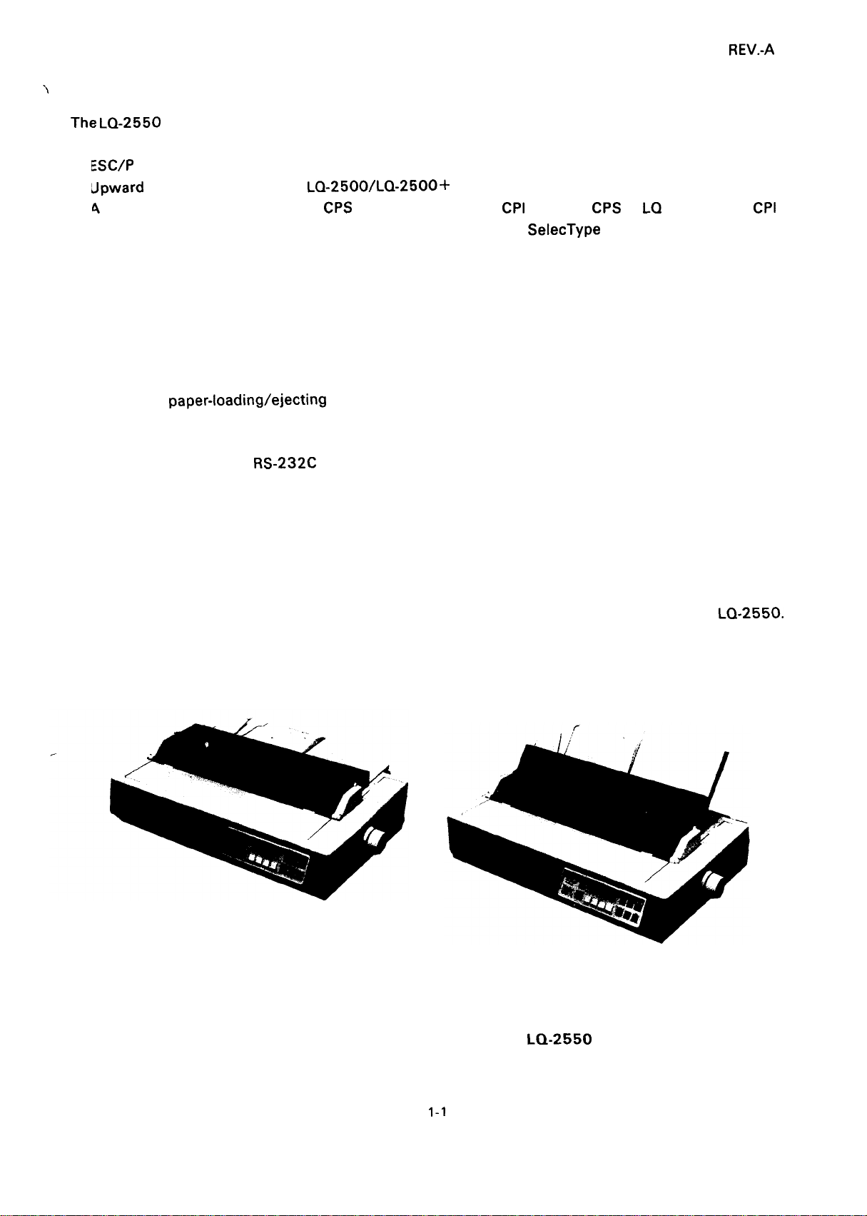
1.1 FEATURES
The
LQ-2550 printer is a multifunction, 24-pin, impact dot-matrix printer. The main features Of this
printer are:
ESC/P
●
I
I
●
●
●
●
●
●
●
●
●
●
●
●
Expanded is implemented as a standard
Upward
A
maximum print speed of 400
I
Direct selection of font, pitch, and normal/condensed mode, and SelecType function with LCD (Liquid
Crystal Display) which makes panel settings easier
Multiple standard fonts (Roman, Saris Serif, Courier, Prestige, Script, OCR-A, and OCR-B)
Advanced paper handling:
Automatic release function
Automatic platen gap adjustment function
Micro adjustment function
Tear-off function
Automatic
Color printing capability
Low-noise acoustics
Both 8-bit parallel and
Push and (optional) pull tractor feeding ,
Printing of fanfold paper without removal of the cut sheet feeder (option)
Optional interface for the EPSON 8100 series
Optional low-priced, double-bin cut sheet feeder with envelope feeding capability
compatibility with the
paper-loading/ejectin9 function
LQ-2500/LQ-2500+
CPS
in draft mode at 12
RS-232C serial interfaces
CPI
and 133
CPS
in LQ mode at 12
REV.-A
CPI
Figure 1-1 shows exterior views of the printer, Table 1-1 lists optional units that are available, and Table
1-2 lists the optional interface boards (refer to Chapter 3 for more detailed information) for the
Setting for Continuous Paper
Setting for Cut Sheet Paper
LQ-2550.
Figure 1-1. Exterior Views of the
1-1
LQ-2550
Page 10
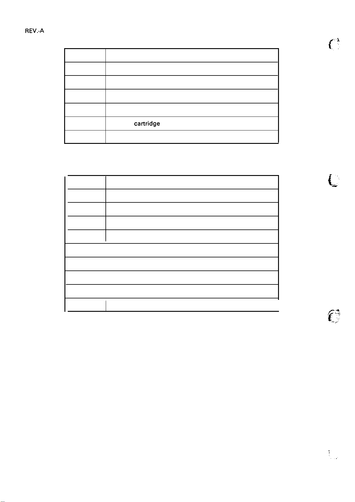
Table 1-1. Optional Units
No.
#73 14
#7343
#7394 Scanner option kit
#7762
#7763
#7764
No.
#8143
#8145 RS-232C current loop interface type II
#8 148 Intelligent serial interface
Name
Pull tractor unit
Double bin cut sheet feeder
Ribbon cartridge (black)
Ribbon
Ribbon cartridge (film-black)
Table 1-2. Optional Interface Boards
Name
New serial interface
cattridge (color)
... ,
{:’”
#8 149 Intelligent serial interface type II
#8 149M
#8 161
#81 65
#8 172
#8 172M 128K-byte buffer parallel interface
Intelligent serial interface type Ill
I
IEEE-488 interface
I
Intelligent IEEE-488 interface
I
32 K-byte buffer parallel interface
I
I
g:;;
.7,
...,
1-2
Page 11
\
1.2 SPECIFICATIONS
The LQ-2550 communicates with a wide variety of host computers, with the aid of the optional Identity
Modules. However, this section describes the specifications for the printer without the Identity Module.
Specifications not affected by firmware (hardware specifications) are the same whether or not the
Identity Module is installed.
1.2.1 Hardware Specifications
REV.-A
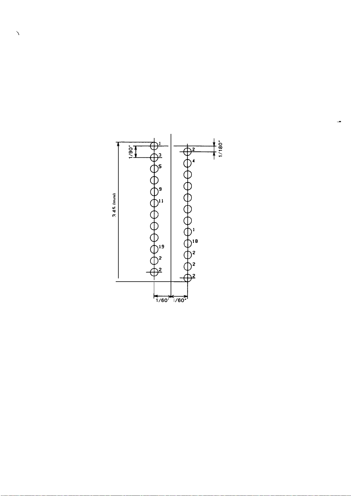
Printing
Pin Configuration
Method
Serial, impact dot matrix
See Figure 1-2 (1 2x2 staggered, diameter: 0.2 mm).
0
OJ
\
5
=’
7
$
11
13
15
17
I
1’
21
23
$’-
2
4
6
8
10
12
14
16
la
20
22
24
..=
4
1160”
Figure 1-2. Printhead Pin Configuration
1-3
Page 12
REV.-A
Feeding Method
Friction feed
Tractor feed (push: standard, push-pull: optional)
NOTES: 1. When using friction feed:
● Select friction feed on the control panel.
● Do not use continuous (fanfold) paper.
● Do not use a single sheet paper shorter than 92mm or longer than 364mm
● Do not perform any reverse paper feed operations within the top 8.5 mm and bottom
22 mm of the paper.
● Do not perform reverse feed beyond 1/6” after the paper end has been detected.
● Do not use multi-part, single-sheet forms.
2. When using push-pull tractor feed:
● Select tractor feed on the control panel.
● Mount the pull tractor unit (optional).
● Do not loosen the paper between the platen and the pull sprocket.
● Precisely align the horizontal position of the pull sprocket and push tractor.
● Do not perform reverse feeding for more than 1/6”.
● Do not perform reverse feeding after the paper end has been detected.
● Multiple copy paper must be pasted together using line or dots.
● Copy paper must be carbonless multi-part paper.
Paper Loading Directions
Fanfold paper
Cut sheet paper
Line Spacing
Line Feed Speed
Feeding Method
Friction without
Friction with
Tractor
=
Inserted from the rear
Inserted from the top
1/6”, 1/8”, or programmable in units of 1/1 80”
See Table 1-3.
Table 1-3. Line Feed Speeds
1/6” line spacing
Continuous
[ins/line] [inch/s]
CSF
CSF
84 4.0
orl/360”
1-4
Page 13
\
Paper Specifications
Cut sheet paper
Refer to Table 1-4 and
REV.-A
Figure 1-3.
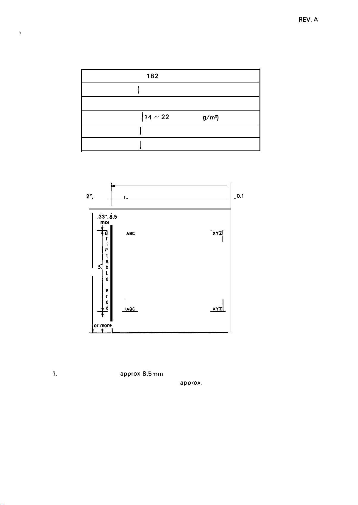
Table 1-4. Cut Sheet Paper
Width
Length
Thickness [mm]
Weight
Quality
Copies
0.1
2“,
3 mm.
or more
.33”, 6.5
r
mol
t
mm
[mm]
[mm]
[lb]
7.2-14.3”,
1-
Specified Conditions
-364 (7.2 - 14.3”)
182
I
I
364 (14.3”) max.
0.065-0.10 (0.0025 - 0.004”)
I
I 14-22
I
Plain paper
I
Not available
(52 -82
182 ’364 mm
Printable area
g/m2)
1
I
-0.1
2“, 3
or more
mm
NOTES:
XYZ
T
XYZ
J
t
MAX. . .
364mm
3;
v
r
i
n
t
I
e
a
r
e
a
ABC
T
ABC
L
1
0.52”,
1.
Printing is possible approx.
accuracy can not be assured in the area
Printing is possible approximately 45.9mm past the point where end-of-page has been
2.
detected. Thus, the value 13.3mm (0.52”) (lowest print position) is given for reference only.
Paper feed accuracy cannot be
bottom of the page.
3mm
8.5mm
(0.33”) from the top of the paper. But the paper feed
approx. 22mm (0.87”) from the top of the paper.
assured in the area approximately 22mm(0.87”) from the
Figure
1-3. Cut
Sheet Paper Printable Area
1-5
Page 14
REV.-A
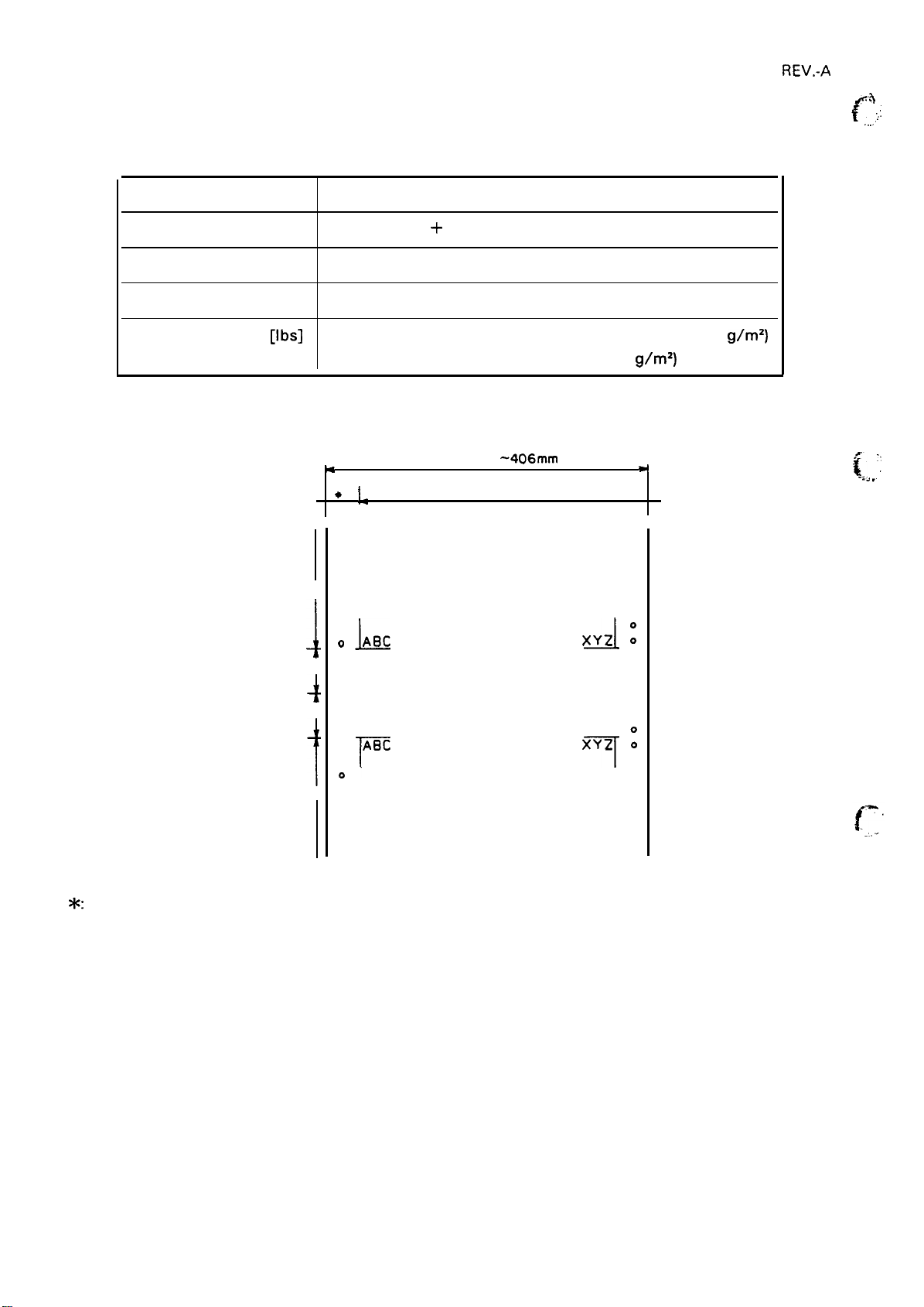
Fanfold paper
Width
Copies
Quality
Total Thickness [mm]
Weight
Refer to Table 1-5 and Figure 1-4.
Table 1-5. Fanfold Paper Specified Conditions
-406 (4.0 - 16.0”)
[mm]
[sheets]
101
6 (1 original + 5 ) over the entire temperature range
Plain paper
0.06-0.46 (0.0023 -0.0 18“)
IIbs]
Printable
area
0.35”, 9 mm
or more
0.35”, 9 mm
or
more
Printable
area
1 sheet . . . . . . . . . . . . . . . . . . . . . . . . . . . . . . . . . . . . . . . . . . . . . . 12
6 sheets ...................12
M
i
4
i
4-16” ,
*
~
o
0
0
0
0
0
0
o
ABC
L
o
0
0
-----------------------------
o
0
0
o ABC
o
T
0’
0
0
0
0
0
Printable area
-15 (40 - 58.2
101
-4C)6mm
-22 (40 -82
g/m2)
d
*
I
0
0
0
0
0
0
XYZ
XYZ
:
d
0
0
0
0
0
:
0
T
o
0
0
0
0
0
g/m2)
each sheet
.“3
f ~
. . . . .
{ ;
.., ,.
,,.
*:
101 - 381 mm (4 -
15“) wide paper . . . . . . . . . . . . . . . . . . . . . 13mm or more,
406 mm ( 16“) wide paper . . . . . . . . . . . . . . . . . . . . . 26mm or more
Figure 1-4. Fanfold Paper Printable Area
1-6
Page 15
.
.
REV.-A
Envelopes
Size
No. 6 165 x 92 mm (6.5 x 3.63”)
No. 10241 x 105mm (9.5 x 4. 13“)
Quality
Thickness
Bond paper, xerographic copier paper, airmail paper
0.16-0.52 mm (0.0063 -0.01 97”)
NOTE: Differences in thickness within printing area must be less than 0.25 mm (0.0098”).
g/m2)
Weight
12- 24 lb (45
-91
\
NOTES: 1. Envelope
2. Keep the
printing is only available at normal temperature.
longer side of the envelope horizontal.
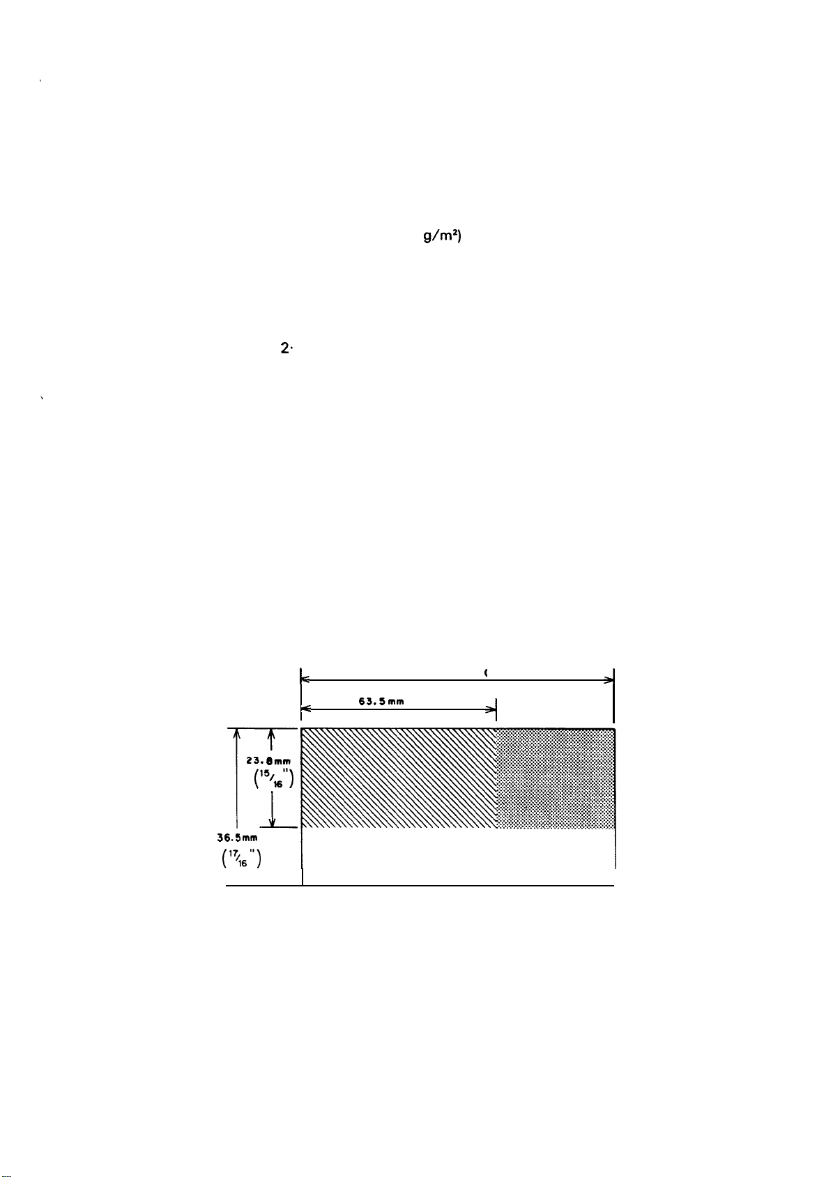
Labels
2.
Size
Thickness
1/2 X 15/1 6“, 4 X 15/1 6“, 4 X 1“7/16“
O.19 mm (0.0075”) max.
NOTE: Thickness excluding the base paper must be less than or equal to 0.12 mm (0.0047”).
NOTES: 1.
Printing of labels is only possible at normal temperature.
Labels must be fanfold.
2.
Labels with pressure-sensitive paper must be joined by dot or line pasting, and the total
3.
thickness must be less than or equal to 0.3 mm (0.01 1 8“) and should be printed under
conditions between 5 to 35 ‘C and 20 to 80% RH.
4.
Examples of labels: AVERY CONTINUOUS FORM LABELS
AVERY MINI-LINE LABELS
Printable
area
See Figure 1-5.
r
36.5mm
(176”)
23.
(’5+6”)
J_
101.6 mm
Emm
k
<
63.5mm (2 ”}2”)
Figure 1-5. Label Printable Area
[
4“ )
A
1-7
Page 16
REV.-A
Ribbon
Ribbon Model No.
Type
Color
Life
[million/characters]*’
xl: LQ-selftest
Dimensions
Weight
Cartridge
See Table 1-6.
Table 1-6. Ribbon Cartridge Specification
I
#7762
Normal
Black
3
See Table 1-7 (Details are shown in Figure A-59.)
See Table 1-7.
Table 1-7. Dimensions and Weight
#7764 #7763
Film
0.2
[
Multi-color
Black, Cyan,
Magenta, and yellow
Black: 1
Cyan: 0.7
Magenta: 0.7
Yellow: 0.5
c
.4
. . .
‘
Width [mm] Height [mm]
676
NOTE: Including the paper feed knob and paper guide.
Electrical Specifications See Table 1-8.
Table 1-8. Electrical Specifications
Voltage ~ AC] 108- 132
Frequency Range [Hz]
“’
Rating Current
Insulation Resistance
[M ohm] min.
(between AC line and chassis)
Dielectric Strength ~ AC, rms]
(1 minute, between AC line and chassis)
[A]
198
Depth [mm]
100-
f
I
535
120
V
1.6
10
1250
Version
Weight [Kg]
(approx.)
20
220-240 V Version
I
49.5 -60.5
I
198-264
1.0
3750
f-
,,.,,
-..+,
*1:
At draft-selftest printing.
1-8
Page 17
REV.-A
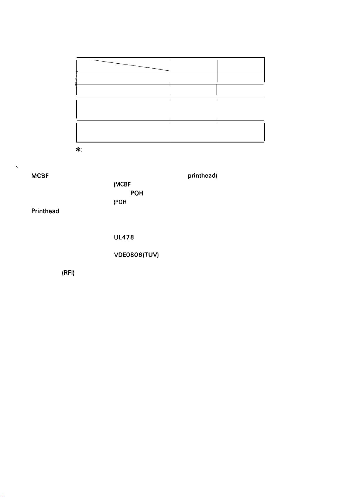
Environmental Conditions
I
x: With shipment container
‘.
Reliability
MCBF
MTBF
Printhead life
Refer to Table 1-9.
Table 1-9. Environmental Conditions
Temperature [“C]
Humidity [% RH]
Resistance to shock [G]
1 (within 1 ms)
Resistance to Vibration [G]
(55 Hz, max.)
5 million lines (excluding
(MCBF . . .
6000
(POH
200 million strokes/wire
Mean Cycles Between Failure)
POH
(duty 25%)
. . .
Power On Hour)
Storage
–30 - 65*
1
5-85
0.50
printhead)
Operating
5-35
10-80
2
1
I
I
0.25
Safety Approvals
Safety standards
Radio frequency
Interface
(RFI)
UL478 (U.S.A. version)
CSA22.2#154
VDE0806 (TUV)
FCC class B (U.S.A. version)
VDE0871 (self-certification)
(European version)
(European version)
1-9
Page 18

REV.-A
1.2.2 Firmware Specifications
Control Code
Printing Direction
Input Data Buffer
Character Code
Character Set
Family
Font and Character Spacing Roman:
Printing Mode
NOTE: A condensed mode for 15
ESC/P-83 Expanded
Bidirectional logic
8K-bytes
8 bits
96 ASCII and 13 international character sets
Roman:
SansSerif:
Courier:
Prestige:
Script:
OCR-B:
OCR-A:
SansSerif:
Courier:
Prestige:
Script:
OCR-B:
OCR-A:
Draft:
Printing quality
Character pitch (10, 12, 15
Condensed
Double-width
Double-height
Emphasized
Double-strike
Italic
Underlined
Outline
Shadow
CPI
seeking
No. O
No. 1
No. 2
No. 3
No. 4
No. 5
No. 6
10, 12, 15, Proportional
10, 12, 15, Proportional
10, 12, 15, Proportional
10, 12, 15, Proportional
10, 12, 15, Proportional
10, 12, Proportional
10, 12 Proportional
10, 12, 15
(Draft/LQ)
CPI
or Propotiional)
characters is not available.
f’
-+
- ,:
Print Speed Refer to Table 1-10.
1-10
Page 19
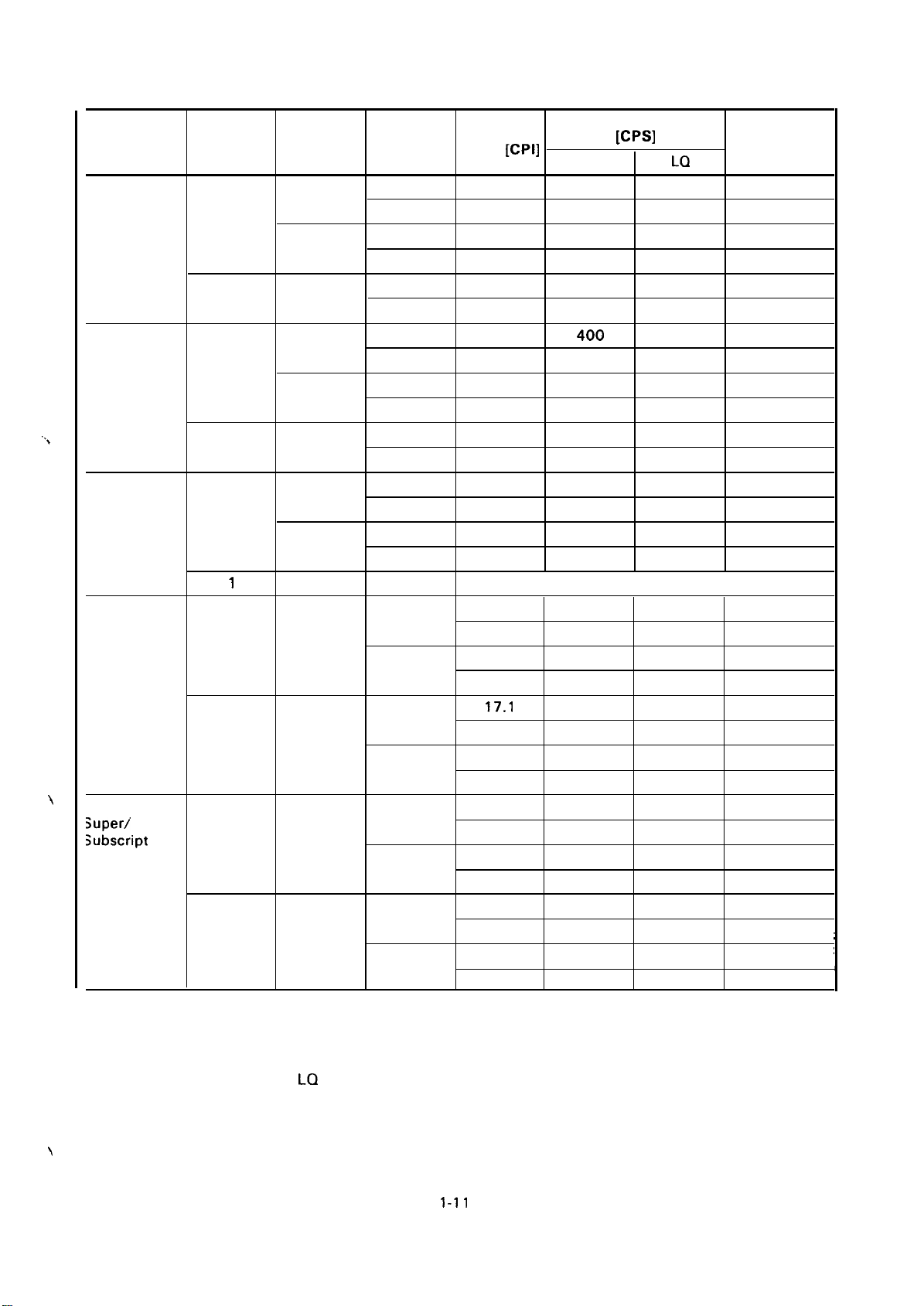
Table 1-10. Printing Mode
REV.-A
.,,
\
Print
Pitch
10 0
12
15
‘proportional
‘proportional
Superl’
subscript
Condensed Emphasized
0
1
1
0 0 0
1
0 0 0
1
o
1
o
1
x
1
x
1
x x
x
x
x
x
Double
Width
0 10
1
0
1
o
1
1
0
1
o
1
1
0
1
o
1
o 17.1
1
o
1
o
1
Pitch
Character
ICPI] Columns
5
Draft
333
167
10 167
Printing
5
17.1
8.5 142 94 116
12
6
12
6
20 333 221 272
10 167
15
15
7.5 250 167
7.5 124
8.6 —
20 221
4.3
10 111
40
8.6 —
20
12.8 —
30
6.4 —
15
25.7 —
60
12.8
30
83
285 189 233
400
200 67
200 133 163
100
500 167
250
[CPS]
Ignored
Speed
LQ
111
55 68
111
55
133 163
67
111
83
83 102
94 Max. 116
50
189 Max. 233
444 Min. 544
94
221
142
333 Min. 408
71
167
285 Max. 174
667
142
333 Min. 204
Printable
Min. 272
Max. 58
Min. 136
Max. 116
Min. 272
Max. 174
Max. 87
Min. 204
Min. 816
Max. 87
136
136
68
81
81
136
204
204
102
;
~
4
NOTES: 1. Max. means the value when the maximum width characters are printed.
2. Min. means the value when the minimum width characters are printed.
3. “
—“ means that
specified.
LQ
character set is automatically selected when proportional pitch is
\
1-11
Page 20
REV.-A
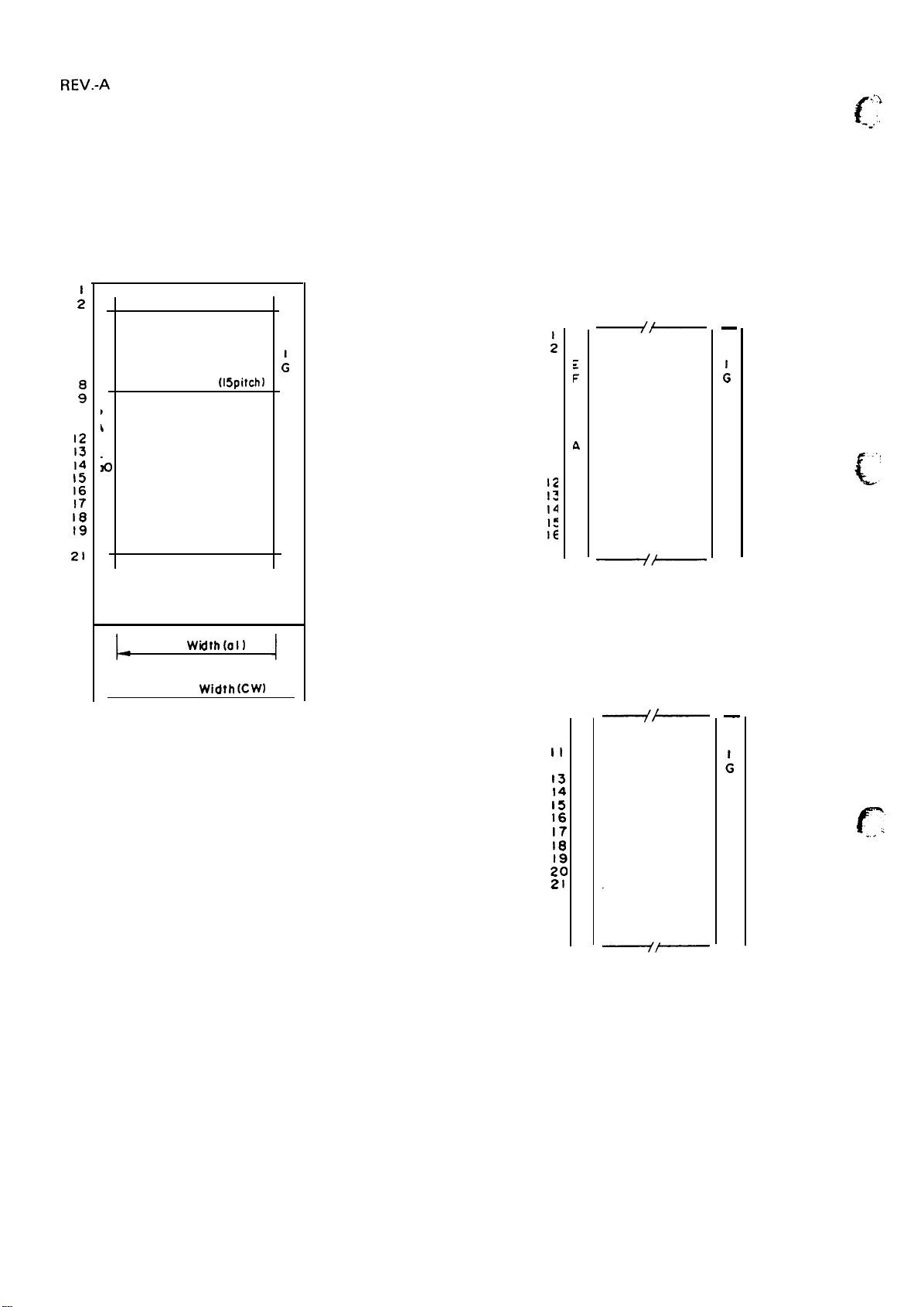
character Matrix
(Normal Character)
See Figure 1-6.
(Superscript Character)
Pin Nos. 17 to 24 are not used for superscript
printing.
. . .
1
,
,
f:
--,
10
II
12
13
14
15
16
17
18
19
20
21
22
23
24
:
3
4
5
6
7
:
Ascender Area
Ascender Area
,
1
L
i)
.
Descender Area
Face
Character
(15pi!Ch)
Wid!h(al)
Width (CW)
4
R
A
H
T
s
P
A
c
E
(a 2
—
10
II
12
I?
14
;
r
3
4
;
5
T
6
7
s
8
P
9
A
c
E
R
k
H
T
s
P
A
c
E
—
(Subscript Character)
Pin Nos. 1 to 8 are not used for subscript printing.
—
R
A
H
T
s
P
A
—
c
E
10
II
12
13
14
15
16
17
18
;:
21
22
23
24
9
L
E
F
T
s
P
A
c
E
—
. .
.
L
r’
... ;
Figure 1-6. Character Matrix
1-12
Page 21
REV.-A
Character Size
See Table 1-11.
Table 1-11. Character Matrix and Character Size
Face
Printing Mode
DRAFT, 10 pitch
DRAFT, 12 pitch
DRAFT, 15 pitch
DRAFT, 10 pitch, condensed
DRAFT, 12 pitch, condensed
LQ,
10 pitch
LQ,
12
pitch 29 X 23 360 2.0 X 3.2
LQ,
15 pitch
LQ,
10 pitch, condensed
LQ,
12 pitch, condensed
LQ,
proportional Max. 39 x 23 360 2.6 X 3.2
I
I
I
I
Matrix
9 X 23
9
X 23
9
X 16 120 1.0 X 2.3 120
. . .
. . .
X 23 360 2.0 X 3.2
29
X 16 360 1.0 X 2.3 180
15
. . .
. . .
Min. 18 x 23 360 1.0
HDD
I
1
120
I
240
240
I
360 I . . .
360
I
I
120 1.9
‘1
. . .
Character Size
H. x V. [mm]
1.9 X 3.2
X 3.2 120
. . .
. . .
X 3.2
Unit
ESC
I
]
120
I
240
240
180
180
I
360
360
180
SP
LQ,
proportional, condensed
LQ,
proportional, super/subscript Max. 28 x 16
LQ
proportional, super/subscript,
condensed
. . .
. . .
Min. 12 x 16 360 0.7
. . .
. . .
360
360
360 1.8
360
360
. . .
. . .
X 2.3
X 2.3
. . .
. .
NOTES: 1. “HDD” means the Horizontal dot density, and the units are dots per inch.
2. “Face matrix” and “character size” indicate the maximum size of characters and this vail
will change with condition of paper.
3. “Unit
4. “...” indicates that the character matrix is reformed
ESC sp” indicates the minimum length which
that can be specified with
becomes half of a non-condensed character.
ESC sp control code.
is added to the right of the character
by printer firmware. Character width
360
180
360
1-13
Page 22
REV.-A
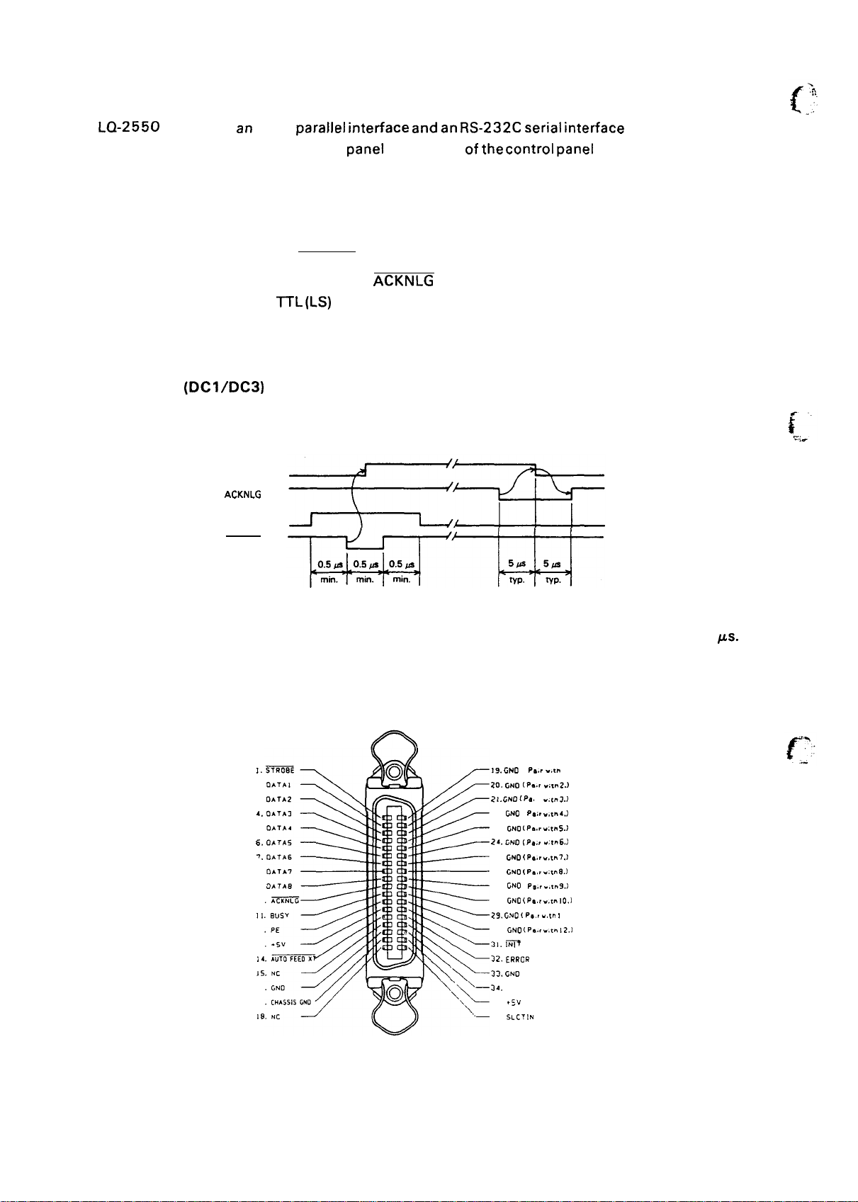
1.3 INTERFACE OVERVIEW
The LQ-2550 has both an 8-bit
interface can be selected from the control
Parallel
interface
Panel
(For details of
1.8.6.2.).
1.3.1 8-bit Parallel Interface Specifications
Data Transmission Mode
Synchronization
Handshaking
Logic Level
Data Transmission Timing
Connector
Connector Pin Assignment
Select/Deselect
(DC1/DC3)
Control
BUSY
ACKNLG
DATA
STROBE
8-bit parallel
By STROBE pulse
By
BUSY and
ITL (LS)
compatible
ACKNLG
See Figure 1-7.
57-30360 (AMPHENOL) or equivalent (See Figure 1-8.)
Refer to Table 1-12.
Refer to Table 1-13.
and an
RS-232C
the control Panel
(either or both)
serial
interface as standard. The
settings, refer to Section
NOTE: Transmission time
Figure 1-7.
(rising and falling time) of every input signal must be less than 0.2
Data Transmission Timing for the 8-bit Parallel Interface
19. GNO
( Pa.,
..,ml.
(Pm.. w,tn2.)
IPa, c w.tn3.)
( Pair
.,,”4.)
(Pa;, w:,n6.)
Pa,. w,,n?.]
w:m8.)
(
Pm,, .,,.9.)
(Pa.<
.,,-12.1
)
l.)
1.
2.
3.
4.
5. 23.
6,
?.
e.
9.
10
II
12
13
14
J5
16
17
19
20.
21.
22.
28,
25.
26.
2’7.
28.
29,
30.
31.
32,
33,
34. NC
3s.
36. SLCTIN
GNO
GNO
GNO
CJNO [Pa., w:tm5.1
GNO
GNO (
GNO ( Per
GNO
GNO (P,., .,,.10,1
GNO ( Par -,. I
GNO
Fit
ERRGR
GNO
.5V
—.
#s.
Figure 1-8. 36-Pin 57-30360 Connector
1-14
Page 23
\
Pin
No.1
1
2
3
4
5
6
7
8
9
Signal
STROBE
DATA1
DATA2
DATA3
DATA4
DATA5
DATA6
DATA7 26
DATA8
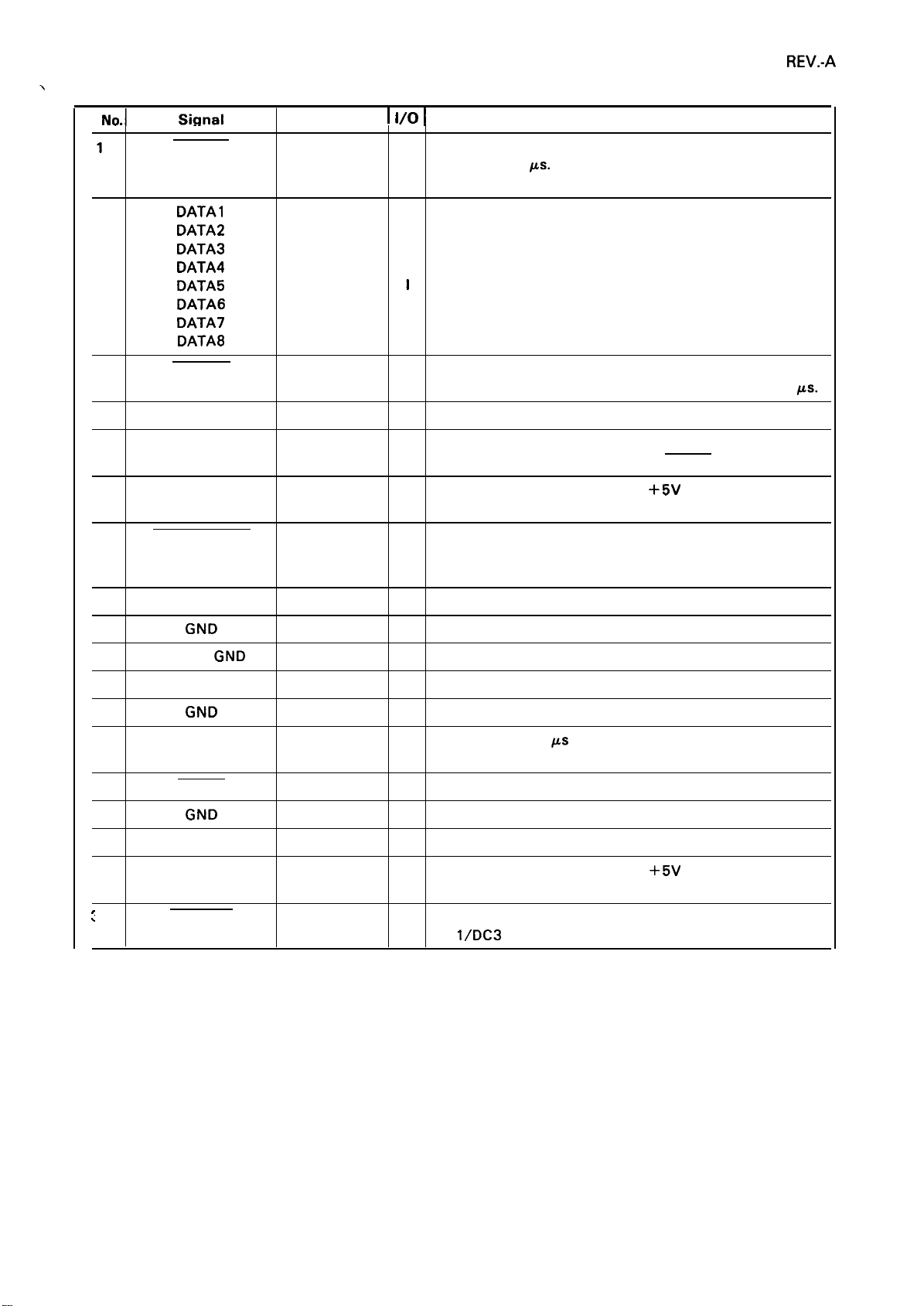
Table 1-12. 8-bit Parallel l/F Connector Pin Assignments
Return
19
20
21
22
23
24
25
27
I 1/0 I
I
Strobe pulse to read the input data. Pulse width must be
more than 0.5
this signal.
I
Parallel input data to the printer.
I
“HIGH” level means data “l”.
I
“LOW’” level means data “O”.
I
I
I
I
I
KS.
Description
Input data is latched after falling edge of
10
11
12
13 SLCT
14 AUTOFEED-XT
15
16
17
18
19
to
30
31
.
.
32
33
.
.
34
.
35
.
#
36
<
ACKNLG
BUSY
PE
NC
GND
Chassis GND
NC
GND
INIT
ERROR
GND
NC
+ 5V
SLECT-IN
28 0 This pulse indicates data are received and the printer is
29 0
30 0
—
—
—
—
—
—
—
16
—
—
—
—
—
ready to accept next data. Pulse width is approx. 11
“HIGH” indicates printer can not accept data.
“HIGH” indicates paper-out.
This signal is effective only when ERROR signal is “LOW”.
o
Always “HIGH”. (Pulled up to
resistor.)
I
If this signal is “LOW” when the printer is initialized, a line
feed is automatically performed by input of “CR” code (Auto
LF).
—
Not used.
— Ground for twisted-pair.
— Printer chassis ground.
— Not used.
— Ground for twisted-pair.
I
Pulse (width: 50 WS min., active “LOW”) input for printer
initialization.
“LOW” indicates that some error has occurred in the printer.
o
— Ground for twisted-pair.
— Not used.
o
Always “HIGH”. (Pulled up to
resistor.)
I
If the signal is “LOW” when printer is initialized, the
DC
l/DC3
control is disabled.
+5V
through 3.3 K ohms
+5V
through 3.3 K ohms
IJS.
NOTES: 1. “Direction” of signal flow is as viewed from the printer.
“Return” denotes “TWISTED PAIR RETURN” and is to be connected at signal ground level.
2.
As to the wiring
never fail to connect the return side.
for the interface, be sure to use a twisted-pair cable for each signal and
To prevent noise, cables should be shielded and
connected to the chassis of the host computer and the printer.
1-15
Page 24
REV.-A
ON-LINE
Sw
OFF-LINE
ON-LINE
SLCT-IN
HIGH/LOW
HIGH
LOW
Dcl/Dc3
DC
l/DC3
DC 1
DC3
DC1
DC3
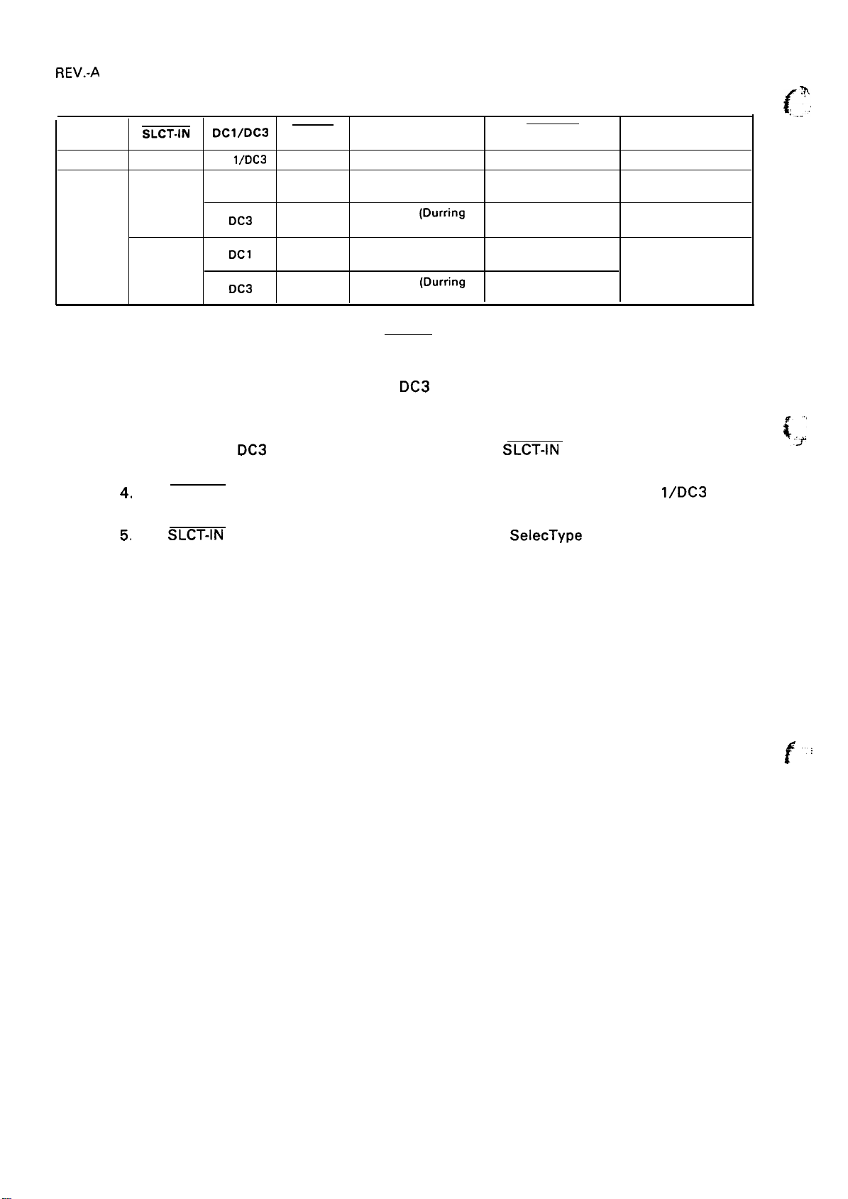
Table 1-13. Select/Deselect Control
ERROR
LOW
HIGH
HIGH
HIGH
HIGH
HIGH
LOW/HIGH (During
data entry)
LOW/HIGH
data entry)
LOW/HIGH (During
data entry)
LOW/HIGH
data entry)
BUSY
(Durring
(Durring
No pulse
Pulse output after Enable
entry)
Pulse output after
entry See Note 2)
Pulse output after Enable (Normal
entry
Pulse output after
entry
ACKNLG
>
(’.
DATA ENTRY
Disable
(Normal Process)
Enable (Waits DC 1.
Process)
NOTES: 1.
2.
3.
4,
5.
In Table 1-13, it is assumed that no ERROR status exists other than that attributable to the
OFF-LINE mode.
Once the printer is deselected by the
DC3
code, the printer will not revert to the selected
state until the DC 1 code is input (In the deselected state, input data is ignored until DC 1
is received.).
The DC 1 and
DC3
codes are enabled only when the
SLCT-IN
signal (Input Connector Pin
No. 36 when the parallel interface unit is used) is HIGH and the printer is initialized.
The SLCT4N signal is LOW when the printer is initialized. At this time the DC
l/DC3
printer
select/deselect control is invalidated, and these control codes are ignored.
The
SLCT-IN
signal is HIGH, and it is not set to LOW by SelecType function when the printer
is initialized. The printer will start from the selected (DC 1 ) state.
(.;
f
.
‘“’
.
1-16
‘. ,
Page 25
1.3.2 RS-232C Serial Interface Specifications
\
Data Transmission Mode
Synchronization
Handshaking
RS-232C serial
Asynchronous
By
DTR
(REV) signal or X-ON/OFF protocol
Refer to Table 1-14 and Figure 1-9.
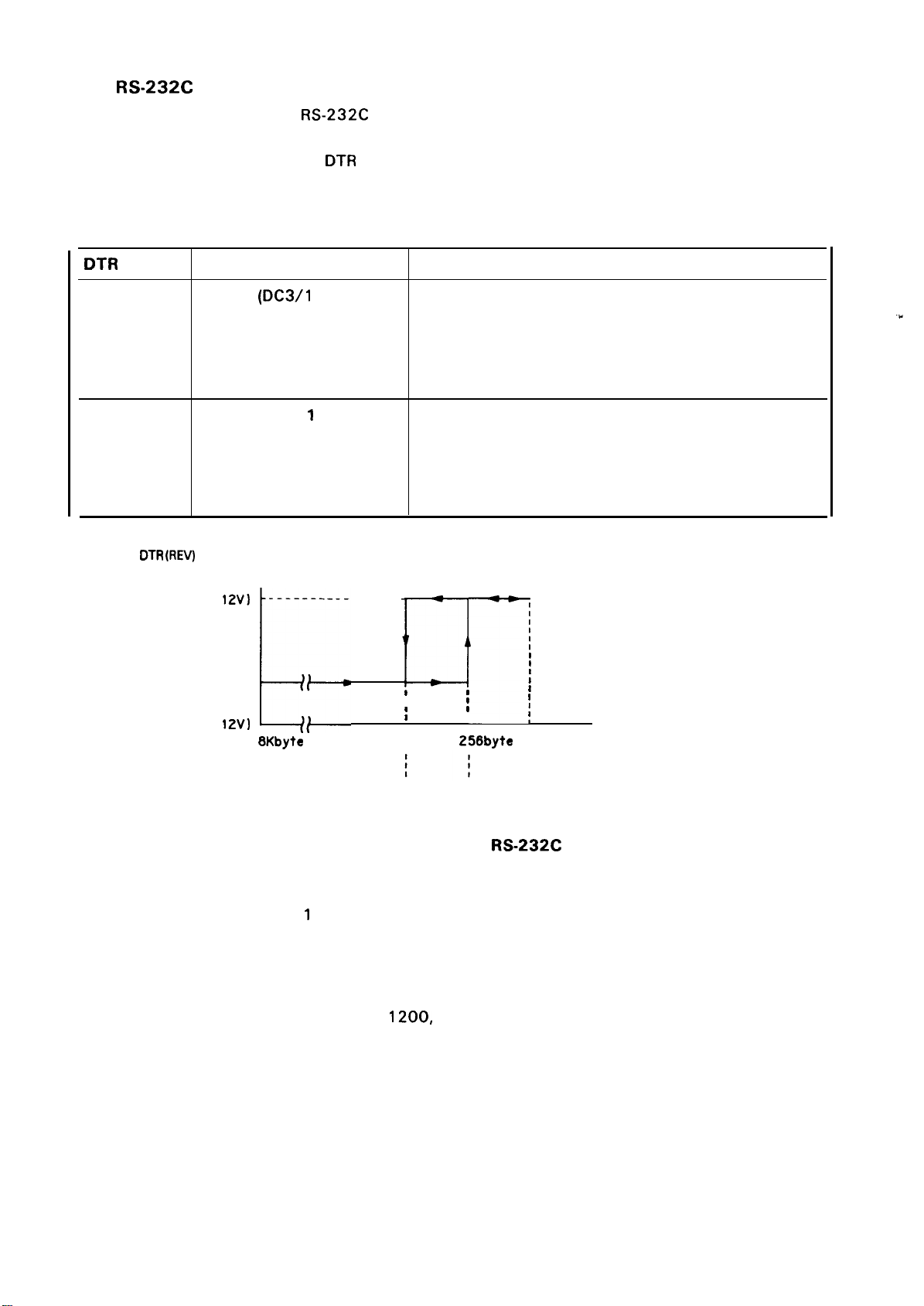
Table 1-14. Serial Interface Handshaking
REV.-A
DTR Signal
MARK
SPACE
DTR {REV)
MARK ( -
SPASE ( +
X-ON/OFF protocol
X-OFF
(DC3\l
3H)
X-ON (DC 1/1 1 H)
Signal
I
12V)
12V)
----------------
L,-
8Kbyte
When the number of bytes remaining in the input
buffer reaches 256 or less, the signal level goes to
MARK, or an X-OFF code is sent to the host computer.
This indicates that the printer is not ready to receive
data.
When the number of bytes remaining in the input
buffer reaches 528 or more, the signal level goes to
SPACE, or an X-ON code is sent to the host computer.
This indicates that the printer is ready to receive data.
I
1
I
I
‘
‘:’
512 byte 256byte O
Description
-.
I
I
I
I
I
I
:
I
I
I
1
‘-
t
I
I
I
byte Input Buffer Vacant Area
Word Length
bit
Start
Data bits
Parity
Stop bits
Bit Rate
Logic Level
X-ON
Figure 1-9. Handshaking for
X-OFF
RS-232C
1
8
Odd, Even, or none
or more
1 bit
1200,
300, 600,
EIA level, MARK: logical 1 (–3 - –27 V)
SPACE: logical O (+3 - +27 V)
2400, 4800, 9600, or 19200 BPS
1-17
X-ON/X-OFF Protocol
Interface
Page 26
REV.-A
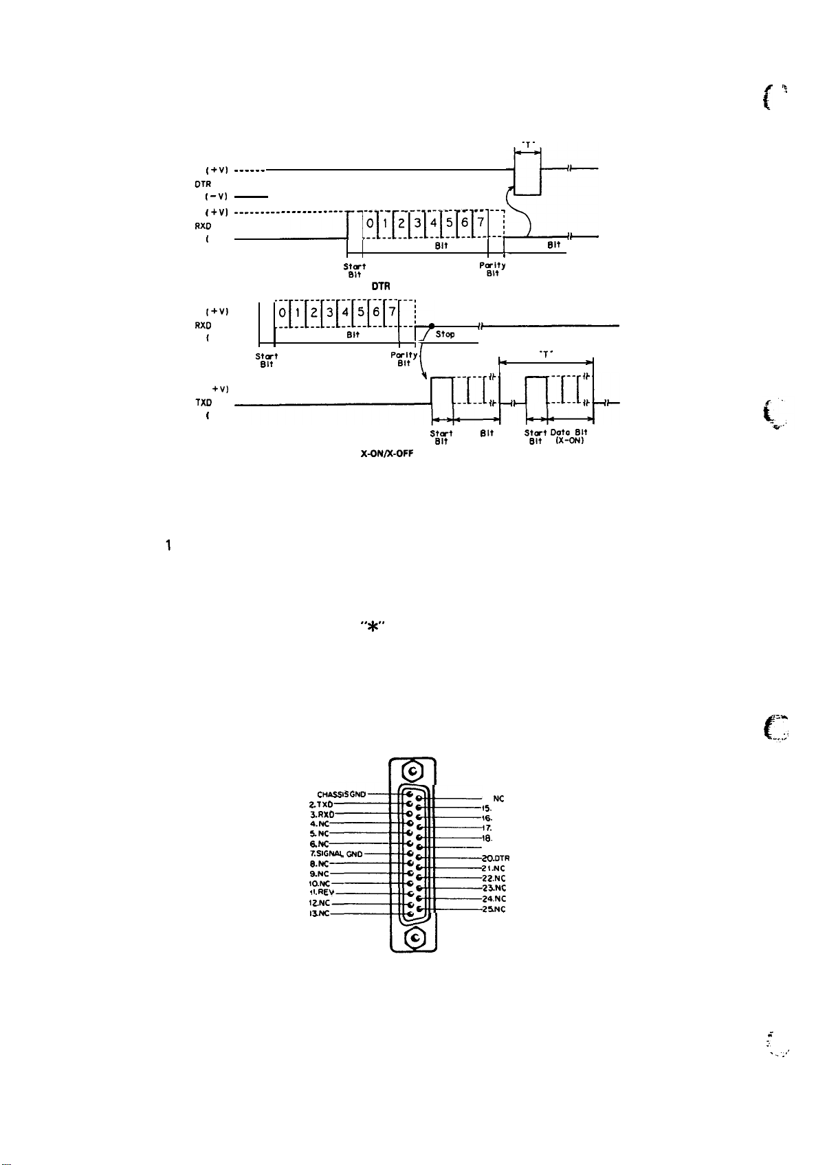
Data Transmission Timing
------
[
+V)
DTR
( -v)
---------------------
(
+V)
RXD
[
-v)
(
+V)
RXO –“
( -v]
(
+V)
TXD
(
-v)
See Figure
1
—-
‘IIM!l!m
Stmf
Blt
1-10.
-- -- -- -- -- -- --
:s!Mik16k
s;t&*
Data
Blt
X-ONDZ-OFF
DTR
Handshake
J
POrli/y
Data
Bit
StW
17
\
.stu-t
Blt
Protocol
Bit
Data
[X-OFF)
--
Pcr:;y
,,—
Blt
--7
.1
1-
L
stop
S::t
Blt
“T-
D~t:at:t
. .
.
~
{
“
...
,’
m
NOTES: 1. The value of “T” varies according to the input data.
2. The word structure of serial data is 1 start bit + 8 data bits + parity (Odd, Even, or none)
1
or more stop bits.
+
Figure 1-10. Serial Data Transmission Timing
Error Detection
Connector
Connector Pin Assignments
Parity error:
Overrun error: Ignored
Framing error: Ignored
D-SUB 25-pin connector (See Figure 1-1 1.)
Refer to Table 1-15.
1. CHA5.51S
Z.TXO
3.RxD
4.NC
5.NC
SAC
7.SIGW
e.Nc
9.NC
to.Nc
t I.REv
IZ.NC
IXNC
—
#
“*”
GND
GNO
is printed.
E
34.
45.
\6.
!7. Nc
18.
19. NC
2D.DTR
2i.NC
Z2.NC
2%NC
Z4.NC
2SNC
NC
NC
NC
Zn
.
.,
f
-..
,,,
Nc
Figure 1-11. Serial Interface Connector
1-18
.-
:.,
. . .,
,’
Page 27

\
Table 1-15. RS-232C Serial Interface Connector Pin Assignments
Pin No. Signal
I
2
20
TXD o
DTR
1/0
o
Transmit data.
Indicates when printer is ready to receive data. “MARK” level
indicates printer is not ready to receive data.
11
3
7
REV(=2nd RTS)
RXD
SIGNAL
1
CHASSIS
GND
GND
—
—
o
I
Same as
Receive data.
DTR.
Signal (Logic) ground level.
Printer chassis ground.
NOTE: “Direction” of signal flow is as viewed from the printer.
\
Description
1-19
Page 28
REV.-A
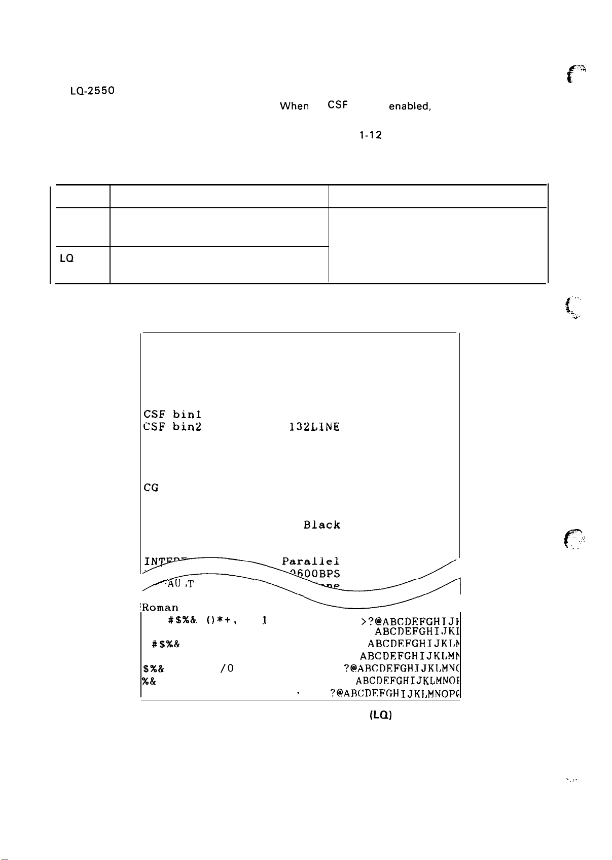
1.4 SELF-TEST OPERATION
-’%
f
The LQ-2550 printer has the following self-test functions. The current and default settings at the control -‘“
panel are printed when the self-test is executed.
is printed out at the end of the first page.
Table 1-16 lists the self-test operating instructions and Figure
Table 1-16. Self-Test Operation
Type-face
Draft
LQ
Turn the power ON while pressing the
LINE FEED switch.
Turn the power ON while pressing the
FORM FEED switch.
Start
Current setting
FONT
PITCH
CONDENSED
FORM
LNG
Tractor 66LINE
CSF
binl
CSF bin2
1“ SKIP
AUTO TEAR OFF
LEFT MARGIN
RIGHT MARGIN
CG
TABLE
COUNTRY
PRINT DIR. Bi-d
COLOR
Default setting
When
the
Roman
10CPI
132LINE
132LINE
Italic
Black
C-SF
mode is
Push the ON LINE switch, and turn the
power OFF.
enabIed,
1-12 shows the self-test printing.
the current sheet length
stop
off
off
off
o
136
USA
# . .
&
.+’
. . .
c“
- ,,. .
.
. .
.
A{]
I
IT
MACRO
1
IRoman
! “
#$%&.
‘ (
)*+,
-. /0 I 234 56789: ; < =
! “ #$%&‘ ( )*+ , -. /01234 56789 : ; < = > ?@
“
#$%&.
‘ ( )*+ ,-. /0123456789 : ; < = > ?@
#$%& ‘ ( )*+ ,-. /0 123456789 : ; < = > ?@
$%&.
‘ ( )*+ ,-. /0 123456789
%&
‘ ( )*+ , -. /0 123456789
& ‘ ( )*+ , -
. /0 1234 56789:
Figure 1-12. Self-Test Printing (LQ)
: ; < = >
: ; < = > ?@!
“
, < = >
1-20
?@i4FWT)J?FGH
ABCI)EFGHIJKLMNOE
?@.A~c:~F.F~H T
I
>?@ABCI)EFcHTJ}
ABCllEFGHI.JKI
ABCDFFGHIJKIIh
A13CDEFGHIJKLMb
IJKl,MN(
JK],MNOPG
. . . . .
Page 29
.,
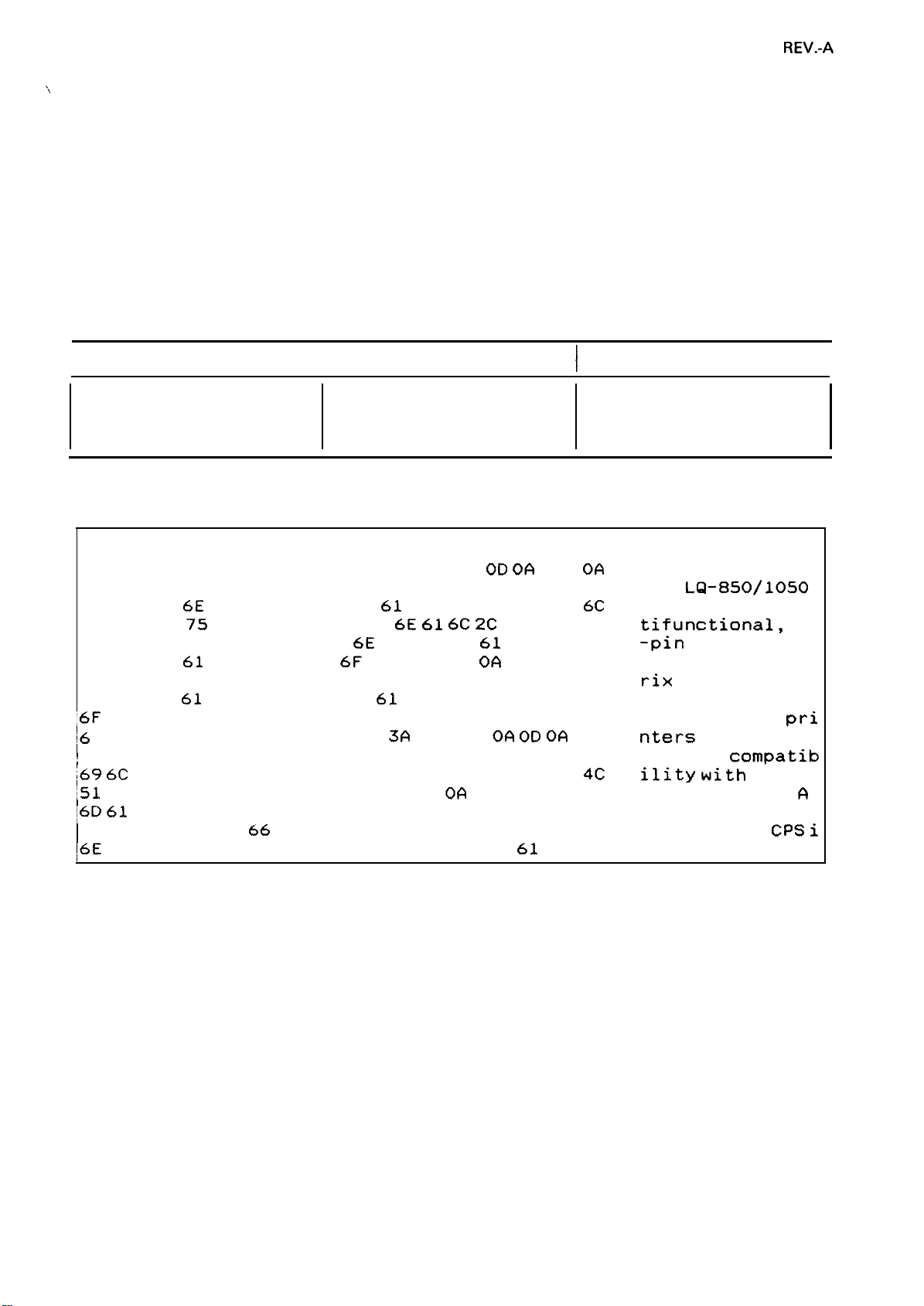
1.5 HEXADECIMAL DUMP FUNCTION
In hexadecimal dump mode, the printer prints out the data it receives in hexadecimal format. The printer
prints a column of 16 hexadecimal values, followed by a column containing the 16 corresponding ASCII
characters. If there is no corresponding printable character for a value (e.g., a control code, such as
a carriage return or line feed), a period (.) is printed in the ASCII column in the position of the code.
Each line of the dump contains 16 values, printed in the order they were received, and any remaining
data (less than 16 values on the final line) can be printed by operating the ON LINE switch. Table 1-17
explains the hexadecimal dump operation and Figure 1-13 shows a sample printout of the operation.
Table 1-17. Hexadecimal Dump Operation
REV.-A
I
Hexadecimal dump mode
\
Data Dump Mode
31 2E 31 20 46 45 41 54 55 52 45 53
54 68 65 20 4C 51 2D 38 35 30 2F 31 30 35 30 20
70 72 69
74 69 66
2D 70 69 6E 20 70 72 69
69 6D 70
72 69 78 20 70 72 69 6E 74 65 72 73 2E 20 54 68
65 20 6D
6F
66 20 74 68 65 20 74 68 65 73 65 20 70 72 69
6
E 74 65 72 73 20 61 72 65 3A 20 OD OA OD OA 2E
~ 20 55 70 77 61 72 64 20 63 6 F 6D 70 61 74 69 62
69
6C 69 74 79 20 77 69 74 68 20 74 68 65 20 4C
51
2D 38 30 30 2F 31 30 30 30 OD
,6D 61 78 69 6D 75 6D 20 70 72 69 6E 74 20 73 70
65 65 64 20 6F
,6E 20 64 72 61 66 74 20 6D 6F 64 65 20
Function
6E 74 65 72 73 20 61 72 65 20 6D 75 6C
75
6E 63 74 69 6F
61
63 74 20 64 6F 74 2D OD 06 6D 61 74
61
69 6E 20 66 65 61 74 75 ‘72 65 73 20
66
20 32 36 34 20 43 50 53 20 69
I
Turn the power ON while Turn the power OFF.
pressing both the LINE FEED
and FORM FEED switches.
6E
Operation
OD 06
6E 61
74 68 65 61 64 2C 20
6C 2C 20 32 34
OA
2 E 20 41 20
61
I
OD
OA
74 20
stop
1.1 FEATURES. . . .
The
LQ-850/1050
printers are mul
tifunctlonal,
-pin
print head,
impact dot- . . mat
rix
printers. Th
e main f eatu res
of the these
nters
ility
Q-800 /1000...
maximum print sp
eed of 264
n draft mode at
are: . . . . .
Upward
with
compatib
24
pri
the L
A
CPS
I
i
Fig 1-13. Hexadecimal Dump List
1-21
Page 30
REV.-A
1.6 PRINTER INITIALIZATION
There are two initialization methods: hardware
1.6.1 Hardware Initialization
This type of initialization occurs when printer power is turned on or when the printer receives the I NIT
signal from the
the following actions:
● Initializes the printer mechanism
● Clears the downloaded character set
● Clears the input data buffer
● Clears the image buffer
● Sets printer selections to their default values (Refer to Section 1.6.3.)
1.6.2
This type of initialization occurs when the printer receives a command
printer is initialized in this way, it performs the following actions:
● Clears the image buffer
● Sets printer selections to their default values
(Several settings are changed by the last
1.6.3.).
host via the 8-bjt Parallel interface. When the
Software Initialization
initialization and software initialization.
winter is
SelecType operation before
initialized in this wwt it Performs
(ESC @)
ESC@
via software. When the
is input (Refer to Section
1.6.3
The default values set by the default setting mode of the
initialization. The printer’s default values are as follows:
Page
Left and Right Margin
Line Spacing
Vertical Tab Positions
Horizontal Tab Positions
VFU Channel
Family Number
Downloaded Characters
Justification
Character Spacing
Bit Image Mode Assignment
Default Values
Position
of Type Style
SelecType
Preset paper position becomes top-of-form position
SelecType setting
1/6”
Cleared
Every 8 characters (relative)
Channel O
SelecType setting
Deselected
Left justification
No additional spacing
ESC
ESC
K =
Z =
ESC *O, ESC
ESC
X3
L =
function are only reset by a hardware
ESC xl, ESC
Y =
ESC X2,
1-22
. .,,
Page 31

REV.-A
‘ 1.7 ERROR CONDITIONS
This section describes the error conditions and buzzer operation of the printer.
AND BUZZER OPERATION
1.7.1 Error Conditions
If any of the following errors occur, the printer automatically enters the OFF LINE mode and outputs
the appropriate interface signal.
● Carriage and platen gap home positons are not detected at printer mechanism initialization.
● The ON LINE switch is pressed, causing the printer to enter OFF-LINE mode.
● Paper-out is detected.
● A paper-out signal is detected after the printer has
cut sheet feeder enabled.
For information concerning the status of the interface signals, refer to Table I-l 2.
perFormed
a paper loading operation with the
1.7.2 Buzzer Operation
. .
The buzzer rings as follows:
When a BEL code is sent to the printer, the buzzer sounds for 0.1 seconds.
●
When an error has occurred,
●
Carriage Trouble:
Paper End:
●
When a panel setting is accepted, the buzzer sounds for 0.1 seconds.
Sounds 5 times (rings for 0.5 seconds with 0.5 second intervals.)
Sounds 3 times (rings for 0.1 seconds with 0.1 second intervals.)
1-23
Page 32

REV.-A
1.8 MAIN COMPONENTS
The LQ-2550 printer includes the following major subassemblies:
●
Model-5560 printer mechanism
●
ROMA board (main board)
●
ROPS/ROPSE board (power supply board, 100- 120V and 220Fan Unit
●
Housing
●
c
ROPNL-W
Figure 1-14 shows
Fan Unit
board
\
(control panel)
LQ-2550 component locations.
the
240V
versions)
Figure 1-14.
LQ-2550
Component Locations
Printer
Mechanism
.
r’
1-24
Page 33

REV.-A
1.8.1 Printer Mechanism
This section describes over view of the printer mechanism, and paper handling and operations.
1.8.1.1 Overview
To improve paper handling, the following functions are newly incorporated in this 24-pin printer in
addition to the conventional ones.
● Automatic release mechanism
● Automatic paper thickness detection nechanism
● Automatic platen gap adjustment mechanism
● Automatic paper width detection mechanism
● Automatic loading lever open/close mechanism
Figure 1-15. Model-5560 Printer Mechanism
-
1-25
Page 34

REV.-A
1.8.1.2 Paper Handling and Operations
Paper Loading and Ejection
Since the paper release lever is controlled automatically, the pApER SELECT and LOAD/EJECT switches
highly
on the control panel provide
(continuous) and single sheet paper and loading/ejecting paper are performed automatically.
a) Single Sheet Loading and Ejection
To load a sheet of paper, press the PAPER SELECT switch and select FRICTION feed. If fanfold paper
is loaded, the paper is ejected backward (automatic back out). Place the page along the paper guide,
and press the LOAD/EJECT switch. This loads the paper at the top-of-form position. If the
LOAD/EJECT switch is pressed after paper has been loaded, it causes the paper to be ejected
forward.
b) Fanfold Paper Loading and Ejection (Back Out)
Set the fanfold paper into the push-tractor unit. To load fanfold paper, press the PAPER SELECT
switch and select TRACTOR feed. If single sheet paper is loaded, the paper is ejected forward and
the fanfold paper is loaded. When the TRACTOR feed has already been selected, pressing the
LOAD/EJECT switch loads the paper automatically to the top-of-form position. If LOAD\ EJECT
switch is pressed after the fanfold paper has been loaded, the printer ejects the paper backward
to the push tractor. To back out several pages, press the LOAD\ EJECT switch several times, since
reverse feed is performed on a page-by-page basis.
improved paper handling. That is, change over between fanfold
f “:;
{;,,
Micro Adjustment Function
In either case a) or b) above, the top-of-form position is adjustable using the MICRO FEED switch (the
LEDs
message “TOF ADJUST” is displayed on the LCD, and the MICRO FEED, V, and A
ofl/1
the FORM FEED switch advances the paper forward in increments
the switch is held down, and pressing the LINE FEED switch moves the paper in reverse in increments
of 1/180”. Moving the paper with these switches is called micro adjustment. The adjusted position
is stored in the memory and remains effective at the next loading even if the power is cycled. But the
tractor feed is selected, the adjusted position is remained even if the power is turned off.
Auto-Tear-Off Function
To enable the auto-tear-off function, select AUTO TEAR OFF using the
function is activated and the PAPER SELECT is FRICTION, paper is fed in the following way: after the
input data buffer becomes empty, while the printer is ON-LINE, the printer feeds the paper so that the
perforation at the form’s end is moved automatically to the tear-off edge of the printer cover. After the
printer has positioned the paper, the message “TEAR OFF ADJUST” is displayed on the LCD, and the
A, and MICRO FEED
V,
adjustment of the tear-off position. The adjusted position is stored in the memory and remains effective
at the next tear-off even if the power is turned off and on. If subsequent data is input to the printer,
the paper will be reversed to its original position automatically and printing will start. If the ON-LINE
switch is pressed (taking the printer OFF-LINE) while the paper is advanced to the tear-off position, then
the printer will reverse the paper to its original position. The manual tear-off function selected by the
TEAR OFF switch is also called a tear-off function.
LEDs
are lit. The FORM FEED and LINE FEED switches are then available for micro
80” continuously as long as
SelecType function. When this
are lit.). Pressing
,:. ,
(-’
J.-,
1-26
.., -.,,.
Page 35

‘1
1.8.2
REV.-A
ROMA
Board (Main Board)
Figure 1-16 shows the
ROMA
board, which contains an HD64 180R1 P6 (main) CPU andaPPD7810HG
(sub) CPU to control the operation of the printer. Driver circuits for the motors, solenoids,
ICS
and sensors are also included on this board. The main
on the ROMA board are:
CPU
●
HD64180R1 P6 (1 3A) . . . . . . . . . . .
●
pPD7810HG
Gate
●
EO5A1OAA (1 4A) . . . . . . . . . . . . . . . . . . .
●
E05A02LA (2A) . . . . . . . . . . . . . . . . . . . . . .
●
E05A09BA
(7B)
. . . . . . . . . . . . . . . . . .
Array
IC
(4B) . . . . . . . . . . . . . . . . . . . . .
8-bit one-chip CPU (main control)
8-bit one-chip CPU (sub control)
Memory management unit
Printhead
data control
Carriage (CR) and paper feed
(MMU)
IC
(PF)
IC
motors phase pulse control unit
(MCU) IC
● E05A09BA
. . . . . . . . . . . . . . . . . . . . .
(3B)
Platen gap
(PG)
and color select
(CS)
motors phase pulse control unit
(MCU) IC
“)
Memory IC
●
EP-ROM
(1 1A) . . . . . . . . . . . . . . . . . . . . . . . . .
●
EP-ROM
(7A) . . . . . . . . . . . . . . . . . . . . . . . . . . .
●
MASK-ROM (1 2A) . . . . . . . . . . . . . . . . . .
●
PS-RAM (9A) . . . . . . . . . . . . . . . . . . . . . . . . . . .
●
ST-RAM* (1OA) . . . . . . . . . . . . . . . . . . . . . . .
x: This memory is backed-up by
Universal
●
M546 10P (1 1 B) . . . . . . . . . . . . . . . . . . . . .
●
S17304
●
STK6981 H (7D) . . . . . . . . . . . . . . . . . . . . .
●
H8D2148
●
STK66082E (1A) . . . . . . . . . . . . . . . . . . .
IC
(7C) . . . . . . . . . . . . . . . . . . . . . . . . . . . .
(2C) . . . . . . . . . . . . . . . . . . . . . . . .
Main CPU program, 256 K-bit
Sub CPU program, 256 K-bit
Character generator, 2M-bit
Buffers, working area, 256 K-bit
Holds status data, panel data, 256 K-bit
a lithium battery.
8-bit parallel interface
CR motor driver
PF motor driver
Head fan
Printhead
(HF)
driver
IC
IC
motor controller and driver
IC
IC
IC
printhead,
LA 3B
)
1A --
,,—
2°C
Figure 1-16.
7A 7B 9A 10A 1 1A 12A
,
-
,
7’D 7C
ROMA
1-27
i
IB
Board
13A
14A
Page 36

REV.-A
1.8.3 ROPS\ROPSE Board (Power Supply Circuit Board)
The power supply circuit board is one of two boards, the
ROPSE
contains a fuse, line filter, and switching regulator circuit. Compact circuitry is made possible by the
use of a DC-to-DC converter.
for 220-
240 V operation. The basic construction of the two boards are the same: each board
ROPS
for 100- 120 V AC operation or
the
. . .
..Y
:\
f ~~•
“-”
. . .
L
ROPS
Board
--+
f“
- ,,,:.,
.’
.-
.—. +
ROPSE
Board
——-————
.-
Figure 1-17.
ROPS/ROPSE
1-28
Board
Page 37

REV.-A
) 1.8.4 Fan Unit
A fan unit is used to lower the internal temperature of the printer. It removes heat within the printer
housing that is generated by the electric circuits.
.
Figure 1-18. Fan Unit
1.8.5 Housing
The housing consists of the upper and lower cases and accommodates the control panel, printer
mechanism, control circuit board, power circuit, and fan unit. The optional cartridges (e.g., font and
identity modules) can be mounted easily without removing the upper case. Figure 1-19 shows the
LQ-2250 housings.
)
.
Figure. 1-19. Housing
1-29
Page 38

REV.-A
1.8.6 Control Panel
This section describes the control panel functions.
1.8.6.1 Hardware Specification
On the control
Crystal Display) as shown in Figure 1-20.
immediately below the illustration.
ON LINE Switch
This switch toggles the printer between ON-LINE and OFF-LINE. If the printer is set OFF-LINE, printing
is stopped and the printer becomes BUSY. This switch is also used in the
ON LINE LED (Green) Lights in the ON-LINE mode. Blinks when the printhead temperature is too high.
Panel, there are
r
0
POWER
0
READY
0
PAPER OUT
o
ON LINE
pig=
twelve
0
TEAR
~
❑
non-locking
fjfyyj
ON
UNE
Figure 1-20. Control Panel
switches, sixteen
The functions of the switches and indicators are given
LCD
FONM
FEEO
LINE FEED
LOAOIE.JfCl
LEDs,
@s$aQ
-,
and a 20-column LCD (Liquid
1
SelecType function.
c
FORM FEED Switch
Pressing this switch
top-of-form position.
adjustment function,
LINE FEED Switch
When the printer is OFF-LINE, the paper advances continuously one line at a time if this switch is pressed
for more than 0.5 seconds. The space between lines of text is set using the line spacing command.
This switch is also used for the micro adjustment function, the platen gap adjustment function, and
SelecType function.
the
LOAD/EJECT Switch
Pressing this switch when the printer is OFF-LINE, loads or ejects the paper (If a page is inserted in the
cut sheet feeder, it is loaded; if a page is already loaded, it is ejected). Details of the paper loading and
ejection process are described in Section 1.8.1.2. This
once while the printer is OFF-LINE, advances the paper
This switch is also used for
and the
SelecType function.
the micro adjustment function, the platen gap
switch is also used in the
ve~ically to the next
SelecType
function.
.,,
(“-
:..
-
1-30
.:
..
...
Page 39

FONT Switch
)
Pressing this switch selects a font, and holding the switch for more than 1.0 second cycles through
the fonts sequentially. The LCD displays the currently selected font.
PITCH Switch
Pressing this switch selects
through the character pitches sequentially. The LCD displays the currently selected character pitch.
CONDENSED Switch
Pressing this switch selects normal or condensed printing.
CONDENSED LED (Green) Lights when condensed mode is selected.
PAPER SELECT Switch
Selects the paper. Each time this switch is pressed, the paper handling method changes in the following
order: TRACTOR, FRICTION,
paper handling.
.) TRACTOR LED (Green) Lights when tractor feed is selected.
FRICTION LED (Green) Lights
CSF LED (Green) Lights when
the
character pitch, and holding
CSF
BIN 1,
when friction feed is selected.
CSF
CSF
BIN2. Each LED and the LCD displays the currently selected
mode is selected.
the switch for more than 1.0 second cycles
REV.-A
TEAR
Advance the paper to the tear-off position. This switch is only effective for the tractor feed (Refer to
Section 1.8.1.2.).
TEAR OFF LED (Orange) Lights when the tear-off function is enabled.
MICRO FEED Switch
Selects or cancels the micro adjustment function. When this function is enabled, the LED on this switch
and the
backward and the FORM FEED switch is used to feed the paper forward. Paper feed performed in this
micro feed mode does not affect the page position control. This function is also used to adjust the paper
loading position and to adjust the paper to meet the tear-off edge (Refer to Section 1.8.1.2.).
)
MICRO FEED LED (Orange) Lights when micro feed is enabled.
PLATEN GAP ADJUST Switch
Selects or cancels the platen gap adjustment function. When this function is selected, three
V,
and decrease the platen gap respectively. The relative platen gap value message is displayed on the
LCD.
+0. 14mm
PLATEN GAP ADJUST LED (Orange) Lights when the platen gap adjustment function is enabled.
OFF Switch
V and A
and the LED on this switch) are lit and the LINE FEED and FORM FEED switches are used to increase
“+”
level means to be widened. “-” level means to be narrowed. The limits of adjustment are
to –O. 1 4mm.
LEDs
are lit. In the micro feed mode, the LINE FEED switch is used to feed the paper
LEDs
(A,
SelecType Switch
Selects or cancels the
switch is lit and the functions of the ON LINE, FORM FEED, LINE FEED, and LOAD/EJECT switches are
changed for the
SelecType
)
LED (Orange) Lights when
SelecType
SelecType function. When the SelecType function is selected, the LED on this
function.
SelecType mode is selected.
1-31
Page 40

REV.-A
Other LEDs
POWER LED (Green) Lights when power is ON.
READY LED (Green) Lights
PAPER OUT LED (Red)
D
a
A V LED (Yellow) Lights the setting for the
when the printer can receive data.
Lights when the paper is at the end.
SelecType,
adjustment functions.
tear-off, micro adjustment, and platen gap
1.8.6.2
This function is invoked when the SelecType switch is pressed (except during ‘printing). When” this
function is invoked, the printer beeps and the message
SelecType function, major functions can be set by operating the ON LINE
(V), and LOAD/EJECT
this mode and returns to the ON-LINE
DEFAULTS” means that MACRO settings or DEFAULT settings will not be stored in the backup memory.
●
The SelecType mode has five menus. While the message “SeiecType MODE” is displayed, every time
the LINE FEED (V) switch is pressed, the main menu of this mode is displayed in the order:
LOAD MACRO
Function in which the settings stored in one of the four macro channels can be read out and set as
the current
CHANGE MACRO
Function in which the current settings can be changed and stored into one of the four macro channels.
The twelve settings and their options are shown in Table 1-18.
SelecType Function
(D) switches. By pressing the SelecType switch the second time the printer exits
Refer to Figure 1-21 for the entire
SelecType settings.
‘“SelecType MODE’”
(a).
is displayed.. In the
FORM FEED (A), LINE FEED
mode. Exiting without performing “SAVE MACRO” or “SAVE
SelecType
operational sequence.
[
“
~’
CHANGE DEFAULTS
Functions in which the default settings shown can be changed. the default settings and options are
shown in Table 1-19.
PRINT OUT SETTINGS
Function in which all settings
CLEAR ALL MACROS
Function which all settings in
in macro channels and the defaults can be printed out.
macro channels are cleared.
.7
,,
. . . . .
.
(’
,.,
1-32
Page 41

CHAPTER 2
OPERATING PRINCIPLES
REV.-A
2.1 General
2.1.1 Connector Descriptions
2.1.2 Printer Mechanism Operations
2.2 POWER SUPPLY CIRCUIT OPERATION
(ROPS/ROPSE Board)
2.2.1
2.2.2 Input Filter Circuit
2.2.3 Rectifier, Smoothing,
2.2.4 Main Switching Circuit 1
2.2.5 +5 V and +12 V Supply Circuit . . . . . . . . . . . . . . . . . . . . . . . . . . . . . . . . . . . . . . 2-31
. . . . . . . . . . . . . . . . . . . . . . . . . . . . . . . . . . . . . . . . . . . . . . . . . . . . . . . . . . . . . . . . . . . . . . . . . . . . . . . . . . . . . . . . . . . . . . . . . . . .
. . . . . . . . . . . . . . . . . . . . .
2.1.2.1 Printing Mechanism
2.1.2.2 Platen Gap Adjustment Mechanism . . . . . . . . . . . . . 2-8
2.1.2.3 Carriage Mechanism
2.1.2.4 Paper
ROPS/ROPSE
and Surge-suppression Circuits . . . . . . . . . . . . . . . . . . . . . . . . . . . . . . . . . . . . . . . . 2-27
2.2.5.1 +5 V Current Limiting and Voltage
Feed Mechanism . . . . . . . . . . . . . . . . . . . . . . . . . . . . . . . . . . . . . 2-16
. . . . . . . . . . . . . . . . . . . . . . . . . . . . . . . . . . . . . . . . . . . . . . . . . . . . . . . . . . . . . . . . . . . . . . . . .
Board Outline . . . . . . . . . . . . . . . . . . . . . . . . . . . . . . . . . . . . . . . . . . . .
. . . . . . . . . . . . . . . . . . . . . . . . . . . . . . . . . . . . . . . . . . . . . . . . . . . . . . . . . . . . . . . . .
. . . . . . . . . . . . . . . . . . . . . . . . . . . . . . . . . . . . . . . . . . . . . . . . . . . .
Regulator Circuits . . . . . . . . . . . . . . . . . . . . . . . . . . . . . . . . . . . . . . . . . . . . . . .
.
. . . . . . . . . . . . . . . . . . . . . . . . . . . . . . . . .
. . . . . . . . . . . . . . . . . . . . . . . . . . . . . . . . . . . . . . . . .
. . . . . . . . . . . . . . . . . . . . . . . . . . . . . . . . . . . . . . . . . . . .
. . . . . . . . . . . . . . . . . . . . . . . . . . . . . . . . . . . . . . . . . . .
2-1
2-2
2-4
2-5
2-11
2-25
.
2-25
2-27
2-28
.
2-32
2.2.6 Main Switching Circuit 2 (+35 V Supply Circuit) . . . . . 2-34
2.2.7 +35 V Current Limiting and Voltage
Regulator Circuits . . . . . . . . . . . . . . . . . . . . . . . . . . . . . . . . . . . . . . . . . . . . . . . . . . . . . . . . . . . . . . . . .
2.2.8 Over Voltage Protection Circuit
2.3 CONTROL CIRCUIT BOARD
2.3.1 Reset Circuit . . . . . . . . . . . . . . . . . . . . . . . . . . . . . . . . . . . . . . . . . . . . . . . . . . . . . . . . . . . . . . . . . . . . .
2.3.1.1 VX (Drive System Pull-up) Voltage
2.3.1.2 Power ON/OFF . . . . . . . . . . . . . . . . . . . . . . . . . . . . . . . . . . . . . . . . . . . . . . . . . . . .
2.3.1.3 INIT Signal Input from CN1 or CN2 . . . . . . . . . . . . . 2-45
2.3.1.4 Font/Identity Module Installation
and Removal . . . . . . . . . . . . . . . . . . . . . . . . . . . . . . . . . . . . . . . . . . . . . . . . . . . . . . . . . . . . . . . . . . . . . .
2.3.1.5 ST-RAM (1 OA) Battery Backup Circuit . . . . . . . . 2-47
2.3.2 interface...... . . . . . . . . . . . . . . . . . . . . . . . . . . . . . . . . . . . . . . . . . . . . . . . . . . . . . . . .
2.3.2.1
2.3.2.2
2.3.3 Control
(ROMA
Supply Circuit . . . . . . . . . . . . . . . . . . . . . . . . . . . . . . . . . . . . . . . . . . . . . . . . . . . . . . .
8-Bit Parallel Interface . . . . . . . . . . . . . . . . . . . . . . . . . . . . . . . . . . . . . . . 2-48
RS-232C
Panel Interface Circuit . . . . . . . . . . . . . . . . . . . . . . . . . . . . . . . . . . . . . . . . . 2-55
Board) . . . . . . . . . . . . . . . . . . . . . . . . . . . . . . . 2-40
Serial Interface . . . . . . . . . . . . . . . . . . . . . . . . . . . . . . . . . . 2-52
. . . . . . . . . . . . . . . . . . . . . . . . . . . . . . . . . . . . . . . . .
.
. . . . . . . . . . . . . . . . . . . . . 2-48
.
2-36
2-39
.
. . . . . . 2-42
.
2-43
.
2-44
.
. . . . . 2-46
2.3.3.1
LED Drive Section
Z.i
. . . . . . . . . . . . . . . . . . . . . . . . . . . . . . . . . . . . . . . . . . . . . . . .
2-56
Page 42

REV.-A
2.3.3.2 Switch Status Read Section
2.3.3.3 LCD Control/Drive Section . . . . . . . . . . . . . . . . . . . . . . . . . . . . . . . 2-58
2.3.4 State Detection and Sensor Signal Input Circuits . . . . . 2-61
2.3.4.1 Reference Voltage Supply Circuit . . . . . . . . . . . . . . . . . . 2-63
2.3.4.2 35 V Line Voltage Detection Circuit . . . . . . . . . . . . . 2-64
. . . . . . . . . . . . . . . . . . . . . . . . . . . .
2-57
,
‘-’,
i..
2.3.4.3
2.3.4.4
2.3.4.5 PW Sensor Circuit
2.3.4.6 PT Sensor Circuit
2.3.4.7 PG HP Sensor Circuit . . . . . . . . . . . . . . . . . . . . . . . . . . . . . . . . . . . . . . . . . 2-69
2.3.4.8 CR HP Sensor Circuit . . . . . . . . . . . . . . . . . . . . . . . . . . . . . . . . . . . . . . . . . 2-70
2.3.4.9 PE Sensor Circuit . . . . . . . . . . . . . . . . . . . . . . . . . . . . . . . . . . . . . . . . . . . . . . . .
2.3.4.10 RL/LD Sensor Circuit
2.3.4.11 Case Open Sensor Circuit
2.3.5
Printhead Control/Drive Circuit
2.3.5.1 E05A02LA Gate Array (2A) . . . . . . . . . . . . . . . . . . . . . . . . . . . . . 2-75
2.3.5.2 Printhead Drive Circuit
2.3.5.3 Relationship Between Paper Thickness
2.3.5.4 Relationship Between the First
2.3.6 HF Motor Control/Drive Circuit
VR1/VR2
Printhead Temperature Detection Circuit... 2-66
and Print Mode
Pulse Width and +35 V Line Voltage . . . . . . . . . . 2-79
Reading Circuit
. . . . . . . . . . . . . . . . . . . . . . . . . . . . . . . . . . . . . . . . . . . . . . .
. . . . . . . . . . . . . . . . . . . . . . . . . . . . . . . . . . . . . . . . . . . . . . . . .
. . . . . . . . . . . . . . . . . . . . . . . . . . . . . . . . . . . . . . . . . . . . . . . . . . . . .
. . . . . . . . . . . . . . . . . . . . . . . . . . . . . . . . .
. . . . . . . . . . . . . . . . . . . . . . . . . . . . . . . . . . . . . . . . .
. . . . . . . . . . . . . . . . . . . . . . . . . . . . . . . . .
. . . . . . . . . . . . . . . . . . . . . . . . . . . . . . . . . . . . . . .
. . . . . . . . . . . . . . . . . . . . . . . . . . . . . . . . . . . . . .
Printhead Drive
. . . . . . . . . . . . . . . . . . . . . . . . . . . . . . . . . . . . . . . .
2-65
2-67
2-68
.
2-71
2-72
2-73
2-74
2-76
2-78
2-80
‘i.,<,’
2.3.7 CR and PF Motors Control/Drive Circuit . . . . . . . . . . . . . . . . . . . . . . 2-82
2.3.7.1
2.3.7.2 CR Motor Control/Drive Circuit . . . . . . . . . . . . . . . . . . . . . 2-84
2.3.7.3 PF Motor Control/Drive Circuit . . . . . . . . . . . . . . . . . . . . . . 2-93
2.3.8 PG and CS Motors Control/Drive Circuits . . . . . . . . . . . . . . . . . . . 2-98
2.3.8.1
2.3.8.2 PG Motor Drive Circuit
2.3.8.3 CS Motor Drive Circuit
2.3.9
PT/RL/LD
2.3.10 Buzzer Drive Circuit
2.3.11 Initialization Sequence . . . . . . . . . . . . . . . . . . . . . . . . . . . . . . . . . . . . . . . . . . . . . . . . . . . . .
E05A09BA
E05A09BA
Solenoid Drive Circuit . . . . . . . . . . . . . . . . . . . . . . . . . . . . . . . . . . 2-104
Gate Array (MCU: 4B)............ . . . . . 2-83
Gate Array (MCU: 3B)............ . . . . . 2-99
. . . . . . . . . . . . . . . . . . . . . . . . . . . . . . . . . . .
. . . . . . . . . . . . . . . . . . . . . . . . . . . . . . . . . . .
. . . . . . . . . . . . . . . . . . . . . . . . . . . . . . . . . . . . . . . . . . . . . . . . . . . . . . . . . . .
2-100
2-102
2-105
.
2-106
LIST OF FIGURES
Figure 2-1.
Figure 2-2. Printer Mechanism Block Diagram
Cable Connections . . . . . . . . . . . . . . . . . . . . . . . . . . . . . . . . . . . . . . . . . . . . . . . . . . . . . . . . . . . . .
..,
,,...,,,,,. ,..,.,....,,,
.,.,
.
2.2
2-4
,.:
c
--J’
..-
$. .,
Z.ii
Page 43

REV.-A
Figure 2-3.
Figure 2-4.
Figure 2-5.
Figure 2-6.
Figure 2-7.
Figure 2-8.
Figure 2-9.
Figure 2-10.
Figure 2-11.
Figure 2-12.
Figure 2-13.
Figure 2-14.
Figure 2-15.
Figure 2-16.
Figure 2-17.
Figure 2-18.
Printing
Mechanism
Printhead Cooling Mechanism
Platen Gap Adjustment Sequence
. . . . . . . . . . . . . . . . . . . . . . . . . . . . . . . . . . . . . . . . . . . . . . . . . . . . . . . . . . . . .
. . . . . . . . . . . . . . . . . . . . . . . . . . . . . . . . . . . . . . . . . .
. . . . . . . . . . . . . . . . . . . . . . . . . . . . . . . . . .
Paper Thickness Detection Mechanism . . . . . . . . . . . . . . . . . . . . . . . .
Paper Thickness Detection Operation
Platen Gap Adjustment Mechanism
Carriage Movement Mechanism
PW Sensor Operations
Ribbon Feed Mechanism
Color Ribbon Strip Selection
Color Select Mechanism
Push Tractor Feeding
Friction Feeding
. . . . . . . . . . . . . . . . . . . . . . . . . . . . . . . . . . . . . . . . . . . . . . . . . . . . . . . . . . . . . . . . . . . .
. . . . . . . . . . . . . . . . . . . . . . . . . . . . . . . . . . . . . . . . . . . . . . . . . . . . . .
. . . . . . . . . . . . . . . . . . . . . . . . . . . . . . . . . . . . . . . . . . . . . . . . . . .
. . . . . . . . . . . . . . . . . . . . . . . . . . . . . . . . . . . . . . . . . . .
. . . . . . . . . . . . . . . . . . . . . . . . . . . . . . . . . . . . . . . . . . . . . . . . . . .
. . . . . . . . . . . . . . . . . . . . . . . . . . . . . . . . . . . . . . . . . . . . . . . . . . . . . . . . .
. . . . . . . . . . . . . . . . . . . . . . . . . . .
. . . . . . . . . . . . . . . . . . . . . . . . . . . . .
. . . . . . . . . . . . . . . . . . . . . . . . . . . . . . . . . . . .
2-5
2-7
2-8
2-8
2-9
2-10
2-11
2-11
2-13
2-15
2-15
2-17
2-18
Paper Release Mechanism Operations . . . . . . . . . . . . . . . . . . . . . . . . 2-21
Paper Loading Lever Open/Close Mechanism
Operation
. . . . . . . . . . . . . . . . . . . . . . . . . . . . . . . . . . . . . . . . . . . . . . . . . . . . . . . . . . . . . . . . . . . . . . . . . . . . . . . .
ROPS/ROPSE Board Block Diagram
. . . . . . . . . . . . . . . . . . . . . . . . . . . .
2-24
2-26
Figure 2-19.
Figure 2-20.
Figure 2-21.
Figure 2-22.
Figure 2-23.
Figure 2-24.
Figure 2-25.
Figure 2-26.
Figure 2-27.
Figure 2-28.
Figure 2-29.
Figure 2-30.
Figure 2-31.
Figure 2-32.
Figure 2-33.
Input Filter Circuit
. . . . . . . . . . . . . . . . . . . . . . . . . . . . . . . . . . . . . . . . . . . . . . . . . . . . . . . . . . . . . . .
2-27
Rectifier, Smoothing,
and Surge-suppression Circuits
Surge Current
Main Switching Circuit
. . . . . . . . . . . . . . . . . . . . . . . . . . . . . . . . . . . . . . . . . . . . . . . . . . . . . . . . . . . . . . . . . . . . . . .
1. . . . . . . . . . . . . . . . . . . . . . . . . . . . . . . . . . . . . . . . . . . . . . . . .2-28
. . . . . . . . . . . . . . . . . . . . . . . . . . . . . . . . . . . . . .
2-27
2-28
Main Switching Circuit 1 Waveforms . . . . . . . . . . . . . . . . . . . . . . . . . 2-30
+5 V and +12 V Supply Circuit
+5 V Current Limiting Circuit
+5 V Voltage Regulator Circuit
Main Switching Circuit 2
+35 V Supply Circuit
. . . . . . . . . . . . . . . . . . . . . . . . . . . . . . . . . . . . . . . . . . . . . . . . .
. . . . . . . . . . . . . . . . . . . . . . . . . . . . . . . . . . . . . . . . . . . . . . . . . . . . . . . .
. . . . . . . . . . . . . . . . . . . . . . . . . . . . . . . . . . . .
. . . . . . . . . . . . . . . . . . . . . . . . . . . . . . . . . . . . . . . .
. . . . . . . . . . . . . . . . . . . . . . . . . . . . . . . . . . . . .
2-31
2-32
2-33
2-34
2-35
Main Switching Circuit 2 Waveforms . . . . . . . . . . . . . . . . . . . . . . . . . 2-35
+35 V Current Limiting and Voltage Regulator
Circuits
PWM Comparison Sequence
. . . . . . . . . . . . . . . . . . . . . . . . . . . . . . . . . . . . . . . . . . . . . . . . . . . . . . . . . . . . . . . . . . . . . . . . . . . . . . . . . . . .
. . . . . . . . . . . . . . . . . . . . . . . . . . . . . . . . . . . . . . . . . . .
2-36
2-37
Over Voltage Protection Circuit . . . . . . . . . . . . . . . . . . . . . . . . . . . . . . . . . . . . . 2-39
ROMA Board Block Diagram
. . . . . . . . . . . . . . . . . . . . . . . . . . . . . . . . . . . . . . . . . . .
2-40
Figure 2-34.
Figure 2-35.
Figure 2-36.
Figure 2-37.
Figure 2-38.
Main CPU Address Map.. . . . . . . . . . . . . . . . . . . . . . . . . . . . . . . . . . . . . . . . . . . . . . . . . .
Sub CPU Address Map
. . . . . . . . . . . . . . . . . . . . . . . . . . . . . . . . . . . . . . . . . . . . . . . . . . . . . .
.
2-41
241
Reset Circuit . . . . . . . . . . . . . . . . . . . . . . . . . . . . . . . . . . . . . . . . . . . . . . . . . . . . . . . . . . . . . . . . . . . . . . . . . . 2.42
Vx Voltage Supply Circuit . . . . . . . . . . . . . . . . . . . . . . . . . . . . . . . . . . . . . . . . . . . . . . . . 2-43
Power ON Reset Timing . . . . . . . . . . . . . . . . . . . . . . . . . . . . . . . . . . . . . . . . . . . . . . . . . . .
2-iii
.
2.44
Page 44

REV.-A
Figure 2-39.
INIT Reset Timing
. . . . . . . . . . . . . . . . . . . . . . . . . . . . . . . . . . . . . . . . . . . . . . . . . . . . . . . . . . . . . . .
2-45
Figure 2-40.
Figure 2-41.
Figure 2-42.
Figure 2-43.
Figure 2-44.
Figure 2-45.
Figure 2-46.
Figure 2-47.
Figure 2-48.
Figure 2-49.
Figure 2-50.
Figure 2-51.
Figure 2-52.
Figure 2-53.
Figure 2-54.
Figure 2-55.
Figure 2-56.
Module Installed/Removed Reset Timing . . . . . . . . . . . . . . . . . . . 2-46
Battery Backup Circuit . . . . . . . . . . . . . . . . . . . . . . . . . . . . . . . . . . . . . . . . . . . . . . . . . . . . .
(8-bit Parallel) Data Transmission Timing . . . . . . . . . . . . . . . . . . . 2-48
8-Bit
Parellel
Interface Circuit . . . . . . . . . . . . . . . . . . . . . . . . . . . . . . . . . . . . . . . . 2-49
8-Bit Parallel Interface Circuit Operation
8-Bit Parallel Interface Timing
DTR Handshaking
X-ON/X-OFF Handshaking
RS-232C
RS-232C
RS-232C
Control Panel Interface Circuit . . . . . . . . . . . . . . . . . . . . . . . . . . . . . . . . . . . . . . 2-55
MSM59371
MSM59371
SED1
SED1
SED1
Serial Interface Circuit . . . . . . . . . . . . . . . . . . . . . . . . . . . . . . . . . . . 2-53
Serial Interface Circuit Operation . . . . . . . . . . . . . . 2-54
Data Transmission Timing . . . . . . . . . . . . . . . . . . . . . . . . . . . . . 2-54
Data Transfer Timing . . . . . . . . . . . . . . . . . . . . . . . . . . . . . . . . 2-56
Block Diagram
200 Block Diagram
200 Command/Data Write Timing . . . . . . . . . . . . . . . . . . . . 2-59
200 Character Code Map
. . . . . . . . . . . . . . . . . . . . . . . . . . . . . . . . . . . . . . . . . . . . . . . . . . . . . . . . . . . . . . .
. . . . . . . . . . . . . . . . . . . . . . . . . . . . . . . . . . . . . . . . . . . . . . . .
. . . . . . . . . . . . . . . . . . . . . . . . . . . . . . . . . . . . . . . . . . . . .
. . . . . . . . . . . . . . . . . . . . . . . . . . . . . . . . . . . . . . . . . . . . . . . . . .
.:...
. . . . . . . . . . . . . . 2-50
. . . . . . . . . . . . . . . . . . . . . . . . . . . . . . . . . . . . . . . .
. . . . . . . . . . . . . . . . . . . . . . . . . . . . . . . . . . . . . .
.
2-47
2-51
2-52
2-52
2-56
2-58
2-60
Figure 2-57.
Figure 2-58.
Figure 2-59.
Figure 2-60.
Figure 2-61.
Figure 2-62.
Figure 2-63.
Figure 2-64.
Figure 2-65.
Figure 2-66.
Figure 2-67.
Figure 2-68.
Figure 2-69.
Figure 2-70.
Figure 2-71.
Figure 2-72.
Figure 2-73.
Reference Voltage Supply Circuit
35 V Line Voltage Detection Circuit
35 V Line Protection
VR1/VR2
Printhead
Printhead
PW Sensor Circuit . . . . . . . . . . . . . . . . . . . . . . . . . . . . . . . . . . . . . . . . . . . . . . . . . . . . . . . . . . . . . . . 2-67
PT Sensor Circuit
Paper Thickness and AN4 Voltage . . . . . . . . . . . . . . . . . . . . . . . . . . . . . . . 2-68
PG HP Sensor Circuit . . . . . . . . . . . . . . . . . . . . . . . . . . . . . . . . . . . . . . . . . . . . . . . . . . . . . . . . . 2-69
CR HP Sensor Circuit . . . . . . . . . . . . . . . . . . . . . . . . . . . . . . . . . . . . . . . . . . . . . . . . . . . . . . . .
PE Sensor Circuit
RL/LD Sensor Circuit . . . . . . . . . . . . . . . . . . . . . . . . . . . . . . . . . . . . . . . . . . . . . . . . . . . . . . . .
Case Open Sensor Circuit . . . . . . . . . . . . . . . . . . . . . . . . . . . . . . . . . . . . . . . . . . . . . . . . 2-73
Printhead
Printhead
Printhead
Reading Circuit
Temperature Detection Circuit . . . . . . . . . . . . . . . . . . 2-66
Temperature and Printing Operation . . . . . . . 2-66
Control/Drive Circuit Block Diagram . . . . . . . 2-74
Drive Equivalent Circuit . . . . . . . . . . . . . . . . . . . . . . . . . . . . . . . . 2-76
Drive Circuit Signal Timing . . . . . . . . . . . . . . . . . . . . . . . . . 2-77
. . . . . . . . . . . . . . . . . . . . . . . . . . . . . . . . . . . . . . . . . . . . . . . . . . . . . . . . . .
. . . . . . . . . . . . . . . . . . . . . . . . . . . . . . . . . . . . . . . . . . . . . . . .
. . . . . . . . . . . . . . . . . . . . . . . . . . . . . . . . . . . . . . . . . . . . . . . . . . . . . . . . . . . . . . . .
. . . . . . . . . . . . . . . . . . . . . . . . . . . . . . . . . . . . . . . . . . . . . . . . . . . . . . . . . . . . . . . .
. . . . . . . . . . . . . . . . . . . . . . . . . . . . . . . . . .
. . . . . . . . . . . . . . . . . . . . . . . . . . . . .
2-63
2-64
2-64
2-65
2-68
.
2-70
2-71
.
2-72
-..>\
f
. .
‘;
Figure 2-74.
First
Printhead
+35
V
Line Voltage . . . . . . . . . . . . . . . . . . . . . . . . . . . . . . . . . . . . . . . . . . . . . . . . . . . . . . . . . . .
Drive Pulse Width and
2-iv
.
2-79
. .
,.’
Page 45

REV.-A
Figure 2-75. HF
Figure 2-76. HF
Figure 2-77. CR
Figure 2-78.
Figure 2-79. Sub CPU Output Signal and
Figure 2-80. Reference Voltage Generation Circuit . . . . . . . . . . . . . . . . . . . . . . 2-85
Figure 2-81.
Figure 2-82. CR Motor Drive Circuit Signal Timing . . . . . . . . . . . . . . . . . . . . . . 2-87
Figure 2-83. CR Motor Phase Switching Timing
Figure 2-84. Carriage Motion Area . . . . . . . . . . . . . . . . . . . . . . . . . . . . . . . . . . . . . . . . . . . . . . . . . . . .
Figure 2-85.
Figure 2-86.
Figure 2-87.
Figure 2-88.
Figure 2-89. PG and CS Motors Drive Circuit Block Diagram.. 2-98
Figure 2-90. PG Motor Drive Circuit
Motor Control/Drive Circuit
Motor Control/Drive Circuit Signal Timing . . . . . . 2-80
and PF Motors Control Circuit Block
Diagram
TMI
CR Motor Drive Circuit
High Speed Skip. . . . . . . . . . . . . . . . . . . . . . . . . . . . . . . . . . . . . . . . . . . . . . . . . . . . . . . . . . . . . . .
PF Motor Drive Circuit . . . . . . . . . . . . . . . . . . . . . . . . . . . . . . . . . . . . . . . . . . . . . . . . . .
PF Motor Drive Circuit Signal Timing . . . . . . . . . . . . . . . . . . . . . . . 2-95
PF Motor Phase Switching Timing
. . . . . . . . . . . . . . . . . . . . . . . . . . . . . . . . . . . . . . . . . . . . . . . . . . . . . . . . . . . . . . . . . . . . . . . . . . . . . . . .
Clock Generation Circuit
. . . . . . . . . . . . . . . . . . . . . . . . . . . . . . . . . . . . . . . . . . . . . . . . . . .
. . . . . . . . . . . . . . . . . . . . . . . . . . . . . . . . . . . . . . . . . . . . . . . . . . .
. . . . . . . . . . . . . . . . . . . . . . . . . . . . . . . . . .
. . . . . . . . . . . . . . . . . . . . . . . . . . . . . . . . . . . . . .
TM1
Signal Timing.. 2-84
. . . . . . . . . . . . . . . . . . . . . . . . . . .
. . . . . . . . . . . . . . . . . . . . . . . . . . . .
2-80
2-82
2-84
2-86
2-89
.
2-91
.
2-92
.
2-94
2-97
2-100
Figure 2-91.
Figure 2-92.
Figure 2-93. Paper Thickness and Platen Gap
Figure 2-94. CS Motor Drive Circuit
Figure 2-95. CS Motor Phase Switching Timing . . . . . . . . . . . . . . . . . . . . . . . . . . . . 2-103
Figure 2-96.
Figure 2-97.
Figure 2-98.
Figure 2-99.
Figure 2-100. Printer Mechanism Initialization Sequence 1.... . . . . . 2-106
Figure 2-101. Printer Mechanism Initialization Sequence 2.... . . . . . 2-107
PG Motor Drive Circuit Signal Timing . . . . . . . . . . . . . . . . . . . . . . 2-100
PG Motor Phase Switching Timing . . . . . . . . . . . . . . . . . . . . . . . . . . . 2-101
. . . . . . . . . . . . . . . . . . . . . . . . . . . . . . . .
. . . . . . . . . . . . . . . . . . . . . . . . . . . . . . . . . . . . . . . . . . . . . . . . . . .
PT/RL/LD
PT Sorenoid Drive Circuit
Buzzer Drive Circuit . . . . . . . . . . . . . . . . . . . . . . . . . . . . . . . . . . . . . . . . . . . . . . . . . . . . . . . . . 2-105
Buzzer Drive Circuit Pulse Timing
Solenoid Drive Circuit
Pulse Timing . . . . . . . . . . . . . . . . . . . 2-104
. . . . . . . . . . . . . . . . . . . . . . . . . . . . . . . .
. . . . . . . . . . . . . . . . . . . . . . . . . . . . . .
2-101
2-102
2-104
2-105
LIST OF TABLES
Table 2-1.
Table 2-2.
Connector Descriptions . . . . . . . . . . . . . . . . . . . . . . . . . . . . . . . . . . . . . . . . . . . . . . . . . . 2-3
Printhead Specifications . . . . . . . . . . . . . . . . . . . . . . . . . . . . . . . . . . . . . . . . . . . . . . . . 2-6
Table 2-3.
Table 2-4.
Table 2-5.
Table 2-6.
HF Motor Specifications . . . . . . . . . . . . . . . . . . . . . . . . . . . . . . . . . . . . . . . . . . . . . . . . 2-7
PT Solenoid Specifications . . . . . . . . . . . . . . . . . . . . . . . . . . . . . . . . . . . . . . . . . . .
PT Sensor Specifications . . . . . . . . . . . . . . . . . . . . . . . . . . . . . . . . . . . . . . . . . . . . . .
Platen Gap Adjustment Mechanism
Specifications . . . . . . . . . . . . . . . . . . . . . . . . . . . . . . . . . . . . . . . . . . . . . . . . . . . . . . .
2-v
.
. . . . . . . . . . . . . 2-10
.
2-8
.
2-8
Page 46

REV.-A
Table 2-7.
PG Motor Specifications . . . . . . . . . . . . . . . . . . . . . . . . . . . . . . . . . . . . . . . . . . . . . . . . . .
.
2-10
Table 2-8.
Table 2-9. ”
Table 2-10.
Table 2-11.
Table 2-12.
Table 2-13.
Table 2-14.
Table 2-15.
Table 2-16.
Table 2-17.
Table 2-18.
Table 2-19.
Table 2-20.
Table 2-21.
Table 2-22.
Table 2-23.
Table 2-24.
PG HP Sensor Specifications . . . . . . . . . . . . . . . . . . . . . . . . . . . . . . . . . . . . . . . . . . 2-10
Carriage Movement Mechanism Specifications . . . . . . . 2-12
CR Motor Specifications
CR HP
PW Sensor Specifications . . . . . . . . . . . . . . . . . . . . . . . . . . . . . . . . . . . . . . . . . . . . . . .
Ribbon Feed Gear Train
Color Select Mechanism Specifications . . . . . . . . . . . . . . . . . . . . . . 2-14
CS Motor Specifications . . . . . . . . . . . . . . . . . . . . . . . . . . . . . . . . . . . . . . . . . . . . . . . . . .
Color Select . . . . . . . . . . . . . . . . . . . . . . . . . . . . . . . . . . . . . . . . . . . . . . . . . . . . . . . . . . . . . . . . . . . . . . . . . .
Paper Feed Mechanism Specifications . . . . . . . . . . . . . . . . . . . . . . . . 2-16
PF Motor Specifications . . . . . . . . . . . . . . . . . . . . . . . . . . . . . . . . . . . . . . . . . . . . . . . . . . .
PE Sensor Specifications
Paper Feeding Method and Paper
Paper Release Mechanism Specifications . . . . . . . . . . . . . . . . . . 2-19
RL Solenoid Specifications
RL Sensor Specifications . . . . . . . . . . . . . . . . . . . . . . . . . . . . . . . . . . . . . . . . . . . . . . . . .
Paper Feeding Method Switch Timing . . . . . . . . . . . . . . . . . . . . . . . . . 2-20
Sensor Specifications
. . . . . . . . . . . . . . . . . . . . . . . . . . . . . . . . . . . . . . . . . . . . . . . . . . .
. . . . . . . . . . . . . . . . . . . . . . . . . . . . . . . . . . . . . . . . . .
. . . . . . . . . . . . . . . . . . . . . . . . . . . . . . . . . . . . . . . . . . . . . . . . . . . . .
. . . . . . . . . . . . . . . . . . . . . . . . . . . . . . . . . . . . . . . . . . . . . . . . . .
. . . . . . . . . . . . . . . . . . . . . . . . . . . . . . . . .
. . . . . . . . . . . . . . . . . . . . . . . . . . . . . . . . . . . . . . . . . . . . . . .
2-12
2-12
.
2-12
2-13
.
2-14
.
2-14
.
2-16
2-16
2-16
2-19
.
2-19
. ,,
L
Table 2-25.
Table 2-26.
Table 2-27.
Table 2-28.
Table 2-29.
Table 2-30.
Table 2-31.
Table 2-32.
Table 2-33.
Table 2-34.
Table 2-35.
Table 2-36.
Table 2-37.
Table 2-38.
Table 2-39.
Table 2-40.
Paper Loading Lever Open/Close Mechanism
Specifications
LD Solenoid Specifications
LD Sensor Specifications . . . . . . . . . . . . . . . . . . . . . . . . . . . . . . . . . . . . . . . . . . . . . . . . .
Paper Loading Lever Open/Close Timing . . . . . . . . . . . . . . . . . . . . 2-23
ROPS/ROPSE Board Ratings
Voltages and Applications . . . . . . . . . . . . . . . . . . . . . . . . . . . . . . . . . . . . . . . . . . . . . . .
State of Module . . . . . . . . . . . . . . . . . . . . . . . . . . . . . . . . . . . . . . . . . . . . . . . . . . . . . . . . . . . . . . . . . .
ST-RAM Conditions with Power ON/OFF . . . . . . . . . . . . . . . . . . 2-47
8-Bit Parallel l/F Signals . . . . . . . . . . . . . . . . . . . . . . . . . . . . . . . . . . . . . . . . . . . . . . . . . .
Switch Status Reading . . . . . . . . . . . . . . . . . . . . . . . . . . . . . . . . . . . . . . . . . . . . . . . . . . . . .
SED1
200 Pin Functions . . . . . . . . . . . . . . . . . . . . . . . . . . . . . . . . . . . . . . . . . . . . . . . . . . .
SED1
200 Command List. . . . . . . . . . . . . . . . . . . . . . . . . . . . . . . . . . . . . . . . . . . . . . . . . .
State Detection Circuit
Sensors List. . . . . . . . . . . . . . . . . . . . . . . . . . . . . . . . . . . . . . . . . . . . . . . . . . . . . . . . . . . . . . . . . . . . . . . . . .
35 V Line Voltage and
VR1/VR2 Values and AN5/AN6 Voltages . . . . . . . . . . . . . . . . . 2-65
. . . . . . . . . . . . . . . . . . . . . . . . . . . . . . . . . . . . . . . . . . . . . . . . . . . . . . . . . . . . . . . . . . . . . . . .
. . . . . . . . . . . . . . . . . . . . . . . . . . . . . . . . . . . . . . . . . . . . . . .
. . . . . . . . . . . . . . . . . . . . . . . . . . . . . . . . . . . . . . . . . .
. . . . . . . . . . . . . . . . . . . . . . . . . . . . . . . . . . . . . . . . . . . . . . . . . . . . . .
ANO
Voltage
. . . . . . . . . . . . . . . . . . . . . . . . . . . .
2-22
2-22
.
2-22
2-25
.
2-25
.
2-46
.
2-51
.
2-57
.
2-58
.
2-59
2-61
.
2-62
2-64
Table 2-41.
Table 2-42.
Printhead Temperature Upper/Lower
and AN 1 Voltage . . . . . . . . . . . . . . . . . . . . . . . . . . . . . . . . . . . . . . . . . . . . . . . . . . . . . . . . . . . . . . . .
Paper State and
AN3
Voltage
Level . . . . . . . . . . . . . . . . . . . . . . . . . . . . . 2-67
2-vi
Limits
.
2-67
.-
“.-
.--’
Page 47

REV.-A
Table 2-43.
Table 2-44.
Table 2-45.
Table 2-46.
Table 2-47.
Table 2-48.
Table 2-49.
Table 2-50.
Table 2-51.
Table 2-52.
Table 2-53.
Table 2-54.
Table 2-55.
Table 2-56.
Table 2-57.
Table 2-58.
PG
Gear Flag an
HP Sensor Flag and
Paper State and PB7 Voltage
RL/LD
Sensor Circuit Signal Status . . . . . . . . . . . . . . . . . . . . . . . . . . 2-72
PA1
Voltage . . . . . . . . . . . . . . . . . . . . . . . . . . . . . . . . . . . . . 2-69
PAO
Voltage . . . . . . . . . . . . . . . . . . . . . . . . 2-70
. . . . . . . . . . . . . . . . . . . . . . . . . . . . . . . . . . . . . .
2-71
Printer Cover State and AN1 Voltage . . . . . . . . . . . . . . . . . . . . . . 2-73
E05A02LA Gate Array Functions
. . . . . . . . . . . . . . . . . . . . . . . . . . . . . . .
2-75
Printhaad Drive Pulse and Paper Thickness . . . . . . . . . . . 2-78
Printhead
Pulse Width, and Print Mode
Coil Drive Cycle,
Printhead
. . . . . . . . . . . . . . . . . . . . . . . . . . . . . . . . . . . . . . .
First Drive
2-78
H8D2148 Input Signal and HF Motor Status . . . . . . . . 2-81
MCU
(4B) Address Allocations . . . . . . . . . . . . . . . . . . . . . . . . . . . . . . . . . . . . 2-83
MCU
POT Terminal States and Carriage Speed . . . 2-85
CR Motor Speed and Phase Switching, System . . . 2-90
Various PF Motor Control Relationships . . . . . . . . . . . . . . . . . . 2-93
MCU (3B)
Motor Control Factors
Address Assignments
. . . . . . . . . . . . . . . . . . . . . . . . . . . . . . . . . . . . . . . . . . . . . . . . . . . .
. . . . . . . . . . . . . . . . . . . . . . . . . . . . . . . . . .
2-99
2-100
Related Factors for CS Motor Control . . . . . . . . . . . . . . . . . . . . . . 2-102
Table 2-59.
Related Factors for
PT/RL/LD
Solenoid Control . . . 2-104
2-vii
Page 48

2.1 GENERAL
REV.-A
This chapter will describe features and operations of the Model-5560 printer mechanism,
power circuit board, ROMA control circuit board and control panel.
In this chapter, the following abbreviations are used:
CR:
Carriage
CS:
Color select
PE: Paper end
PF: Paper feed
PG: Platen gap
PT: Paper thickness
LD: Loading
RL: Release
HP: Home position
HF: Head fan
PW:Paper width
ROPS/ROPSE
2-1
Page 49

REV.-A
2.1.1 Connector Descriptions
Figure 2-1 shows the connection between the ROMA board and other units. Table 2-1 gives general
descriptions of the connectors.
#8C0
-:
‘FANuNITk %
CARRIAGE
HOME POSITION
SENSOR
PAPER THICKNESS
SOLENOID. SENSOR
PAPER END
SENSOR
!.,.
%
{ ~
““””
.. . .
.
L
.
PAPER WIDTH
SENSOR.
COLOR SELECT
MOTOR.
HEAD FAN
%
z
$
23
z
tllHOME IWSITION
T
SOLENOID. SENSOR
>
PRINTHEAD
THERMISTOR
PLATEN GAP
MOTOR
PLATEN GAP
LOADING “
CARRIAGE
MOTOR
PAPERWED
MOlm
MOTOR
SENSOF
. . .
<,’
—
(
r
:
(
(
Figure 2-1. Cable Connections
2-2
Page 50

Table 2-1. Connector Descriptions
Boards
ROMA
Connectors
I
CN 1
I
CN2
I
CN3 Host computer
I
CN4
I
CN5 Font module
I
CN6
CN7
CN8 Control panel
I
I CN9
CN
l-i
I
10
CN1l
I
Host computer
#8 IXX l/F board
Identity/font module
Not
used
Battery unit
I
Printer mechanism
I
Connection
Descriptions
l/F (8-bit parallel)
l/F (option)
l/F
(RS-232C
SLOT A
SLOT B
Memory backup
CS motor, HF motor, and
PW sensor
Printhead (R)
Printhead (F)
serial)
+3V
DC
Pin number
36
I
I
I
I
26
—
32
32
l–
I
I
I
I
2
18
18
18
18
3oPs/
30PSE
CN 12
I
CN 13
I
I CN14 I
CN 15
I
I
CN16
CN 17
CN
18
CN 19
CN20
II
I
CN21 I Uppercase
CN22 ROPS board
I
CN 1
I
I
I
/
External AC power switch
PT solenoid and PT sensor
CR HP sensor
Fan unit
PE sensor
PG motor and PG HP
CR motor
PF motor
LD solenoid and LD sensor
RL solenoid and RL sensor
Case open sensor
+ 5 VDC
Power supply board
&12
VDC +35 DC
sensor
5
3
I
2
2
9
6
6
4
4
3
12
2
CN2
NOTES: Refer to Table A-18 in Appendix for details.
ROMA
board
2-3
r==
Page 51

REV.-A
2.1.2 Printer Mechanism Operations
..%
{
The Model-5560 is a serial printer mechanism equipped with a 24-pin impact dot printhead. This “““
mechanism has various new features to reduce manual paper handling. A block diagram is shown in
Figure 2-2.
+5
+35
Printing Mechanism
@Printhead
@Thermal Sensor
.-.-------------
‘@HF
Motor
@Thermal Sensor
PG Adjust Mechanism
@PT
Solenoid
@PT
Sensor
----------------
‘@PA Motor
@PG
H. P. Sensor
Carriage Mechanism
@CR Motor
@CR H. P. Sensor
@PW
Sensor
----------------
@AS Motor
Paper Feed Mechanism
@PF
Motor
@PE
Sensor
----------------
‘@AL Solenoid
@RL
Sensor
----------------
‘@LD
Solenoid
@LD
Sensor
Printer Mechanism
/
‘
f
<
/
I
c
4
-
I
I
I
I
t
I
I
I
I
I
/
I
I
I
I
I
I
I
I
I
I
I
I
I
I
I
+35
+35
+35 +5
I
+
Driver Circuit
+35
Driver Circuit
A
I
+35
Driver Circuit
A
T
Driver Circuit
+35
Driver Circuit
44
I
I
Driver Circuit
+35
Driver Circuit
+35
Driver Circuit
ROMA Board
f
r
-
*
*
+
.-
*
-
{’-”:’
%“
c
*
-
-
Figure 2-2. Printer Mechanism Block Diagram
2-4
.’
. .
,.
Page 52

2.1.2.1 Printing Mechanism
The printing mechanism consists of two parts: The printing mechanism composed of the
ink ribbon and platen, and the
printhead cooling mechanism composed of the printhead fan.
printhead,
Printing Mechanism
Figure 2-3 shows the printing mechanism.
printhead has 24 wires arranged in two staggered
The
connected to their own wire drive coils. The
printhead
lines (12 wires for each line). These wires are
specifications are listed in Table 2-2.
The basic printing operations are as follows:
The drive signal is sent from the control circuit to the
1.
printhead drive circuit and converted to the
printhead drive voltage (+35 V DC), which causes current to flow through the assigned head driving
coil in the
This magnetism pulls the actuating plate to the iron core, and the dot wire attached to the plate is
2.
printhead. This magnetizes the coil and the iron core.
pushed toward the platen.
The dot wire strikes the inked ribbon and paper against the platen to print a dot on the paper.
3.
4.
When the coil is de-energized, the iron core loses it magnetic force so that the actuating plate returns
to its initial position under the action of the actuating plate spring. After having struck the platen,
the dot wire also returns to its initial position under the action of impact energy and the wire resetting
spring, and is held in contact with the actuating plate until it is driven again.
This is the sequence used to print a dot on the paper.
REV.-A
Wtre
Stopper
Reaatwtg
Spring
Act~ating
Plate Spring
Dot
Wwe
Figure 2-3. Printing Mechanism
Papar
Ribbon
Platen
Mask
2-5
Page 53

Table 2-2. Printhead Specifications
Item
Type
Pin Diameter
Pin Configuration
Dot Pitch
Drive Voltage
Coil Resistance
Drive Frequency
Drive Mode
Thermal Sensor Thermistor
Impact dot
0.2 mm
12 line X 2 col.
1/1 80”
35 VDC
8.6 ohms
2.00 KHz (Max.)
Normal
copy 1 thickness. Refer to section 2.3.5.3
copy 2 for details.
Description
Refer to Figure 1-2.
*
10%
*
10% 25”C, for one coil
The selection is depend on the paper
Built-in
Remarks
2-6
?=..
f ~
.-, .
,,:
Page 54

REV.-A
Printhead Cooling Mechanism
Figure 2-4 shows the
printhead has a built-in thermistor to protect the dot wire drive coils from the high printhead
The
temperatures (which can occur after many hours of continuous printing) which may burn or degrade
them. The
back to the control circuit. This is used for
to about
printhead.
Another thermistor is used to protect the HF motor drive circuit from abnormal heating of the HF motor.
printhead temperature detected by the thermistor is converted into a voltage
40°C, the HF motor (Refer to Table 2-3 for its specif ications.) is turned on to cool down the
printhead cooling mechanism.
printhead protection and, if the printhead temperature rises
Printhead
-
Thermistor
signal
and fed
—.
Figure 2-4. Printhead Cooling Mechanism
Item
Type
Drive Voltage 35 VDC
Coil Resistance
Drive Frequency
Driving Method
Thermal sensor
I
Two-phase 6-pole PM type stepper
motor
~
61 ohms & 7% 25”C, for one coil
1600PPS
I
Constant voltage drive
Thermistor
Thermistor
Table 2-3. HF Motor Specifications
Description
& 120PPS One-phase excitation
I
‘
I
&
1
OYO
I
Built-in
Remarks
2-7
Page 55

REV.-A
2.1.2.2 Platen Gap Adjustment Mechanism
This mechanism sets the platen-printhead gap according to the paper thickness. Figure 2-5 shows the
platen gap adjustment sequence.
NOTE: Also, the gap can be ajusted by control panel operation (Refer to section 1.8.6. 1.).
~--:h
1--, :
Start
Paper Thickness Detection Mechanism
Figure 2-6 shows the paper thickness detection mechanism. The PT sensor lever is driven by the PT
solenoid when it is energized. The distance that the PT sensor lever moves is monitored by the
on the PT sensor, and the detected value is converted into a voltage and transferred to the control circuit.
Table 2-4 lists the specifications of the PT solenoid and Table 2-5 lists the specifications of the PT sensor.
Paper Thickness
Detection
Platen Gap
Adjustment
Figure 2-5. Platen Gap Adjustment Sequence
Platen
-(O&w
Y
PT Sensor Lever
pTsensor ~T”
Printhead Drive
Mode Selection
I
q--O~T
\
\
{
L--pTso,enoid
I
u
Setup Completed
u
1
TCR
Figure 2-6. Paper Thickness Detection Mechanism
Table 2-4. PT Solenoid Specifications
Item
Resistance
Drive Voltage 35
Item
Type Conductive rubber
Drive Voltage
65 ohms
VDC
I
VDC
12
Description
Table 2-5. PT Sensor Specifications
Description
2-8
Remarks
& 10%
*
10%
I
TCR
(Touch Control Sensor)
+ 1.5 V, –2.5 V
Remarks
<-’
. ,
.,
. .
.
Page 56

REV.-A
Figure 2-7 shows the operation of the paper thichness detection mechanism.
When paper is not loaded, point A of the PT sensor lever pushes the platen using shaft B as a fulcrum.
TCR
At this time, point C of the PT sensor lever places pressure on the
TCR
PT sensor to indicate the thickness. Ta is used for this
reading. After paper is loaded, point A of
the paper sensor lever holds the paper against the platen. Tb is used for this
(Touch Control Sensor) in the
TCR
reading.
Platen
PT Sensor Lever
A
TCR
B
(a) When no paper is loaded:
Figure 2-7. Paper Thickness Detection Operation
The control circuit uses Tb -
Ta as the paper thickness, and controls the platen gap mechanism so
as to provide the proper platen gap for the paper.
The control circuit adjusts
width which is divided into three grades
printhead trigger pulses applied to the printhead coils according to the paper
{Refer
to Section 2.3.5.).
/
Tb
(b) When paper is loaded:
2-9
Page 57

REV.-A
Platen Gap Adjustment Mechanism
Figure 2-8 shows the platen gap adjustment mectlanism and Table 2-6
lists
its specifications. The .
rotation of the PG motor is transmitted to the pG gear via the PG reduction gear. The position of the
PG gear is detected by the PG HP sensor (Refer to Figure 2-8(a).).
When the PG gear rotates, it drives carriage guide shaft B. Because carriage guide shaft B is attached
off-center, its rotation varies the
PG Reduction Gear
PG Motor Pinion Gear
printhead-platen
c
~o
&
gap (Refer to Figure 2-8(b).).
PG HP Sensor
4
.
.
‘k.? ~
‘-----/
<.
\,
---~,
:: 1’
&Q
.~
Flag
~.
Carriage Guide Shaft B
PG Gear
(a) PG Motor Gear Train
, Printhead
Platen
!
u
Gap
‘%
f“
. .
‘. .
L“
“
.
Figure 2-8. Platen Gap Adjustment Mechanism
Table 2-6. Platen Gap Adjustment Mechanism Specifications
Motor
PG motor;
I
I
/
Gear
transmission
Refer to Table 2-7.
Table 2-7. PG Motor Specifications
Item
Type Four-phase
Drive Voltage
Hold Voltage
Coil Resistance
Description
48-poie
PM type stepper
motor
VDC
35
VDC
5
I 1250hrns~
7% ]
(b) Platen Gap Adjustment
Driving method
Table 2-8. PG HP Sensor Specifications
I
Remarks
*
1
0’70
&
5°h
25°C,
for
one coil
[
Type
Drive Voltage 5
Guide
Shaft B
e C.w.
- C.c.w.
I
PG HP sensor
Refer to Table 2-8.
Item
Description Remarks
Photo-interrupter
VDC
Sensor
*
5°/0
I
,. .::
,,,
c
*:.,”’
1
Driving
Frequency
Driving Method
400 PPS
Constant voltage
drive
2-2 phase
excitation
1
2-10
.-
“.,
--,
Page 58

REV.-A
2.1.2.3 Carriage Mechanism
This mechanism consists of the carriage movement mechanism, ribbon feed mechanism and color
select mechanism.
Carriage Movement Mechanism
Figure 2-9 shows the carriage movement mechanism and Table 2-9 lists its specifications. The printhead
is mounted on the carriage, and the entire unit is supported by the two carriage guide shafts. The
is
carriage is fixed to the timing belt on one side and
Printing is accomplished by the combination of printing mechanism and carriage movement mechanism
operations.
The print start position is determined by the CR HP sensor when the mechanism is initialized. The PW
sensor monitors paper width so as to prevent printing outside the printable area (See Figure 2-1 O.).
moved when the CR motor drives the timing belt.
Am. /“”’”9 “e”
Figure 2-9. Carriage Movement Mechanism
Paper
~
Platen
d
Carriage Guide Shaft B
PW
Platen
Y
Figure 2-10. PW Sensor Operations
Sens4 ~
“----’-
~
2-11
I
4
;aper
/
Page 59

Table 2-9. Carriage Movement Mechanism Specifications
Motor
CR motor;
Driving Method
Timing belt 1/1
Refer to Table 2-10.
Table 2-10. CR Motor Specifications
Description
200-pole PM type step-
Type
Item
Four-phase
per motor
Drive Voltage 35
VDC
Coil Resistance 2.15 ohms & 10%
Driving Frequency 4000
2667
PPS
PPS
Carriage Per
Step Movement
20’’/step
(MIN.)
Sensor
CR HP sensor
PW sensor
Refer to Refer to
Table 2-11. Table 2-12.
Remarks
*
10’YO
25”C, for one coil
2-2 phase excitation
2000
1333
667
PPS
PPS
PPS
Driving Method Constant current chopper drive
Table 2-11. CR HP Sensor Specifications
Item
Type
Drive Voltage
Photo-interrupter
VDC
5
Description
Table 2-12. PW Sensor Specifications
Item
Type
Drive Voltage
Photo-reflector
5
VDC
Description
1-2 phase excitation
Remarks
&
5’yo
Remarks
&
!55%0
..3,
G
-;’
.,
2-12
Page 60

REV.-A
Ribbon Feed Mechanism
The ribbon feed mechanism consists of the ribbon feed mechanism and ribbon cartridge. Figure 2-11
shows the ribbon feed mechanism.
@
Inked Ribbon
I*
-
—..
Ribbon
/
Ureakmg
:
Spring
Transmis
Ribbon
Ribbon
Drive Gear
Ribbon Feed
1
#
Transmission
~
G~ar B 1
Ribbon Feed
Roller
Ribbon Pressure
%
1=’
I
Ribbon
Cartridge
Figure 2-11. Ribbon Feed Mechanism
The ribbon feed mechanism is mounted on the carriage. The ribbon drive wire is fixed between the
side frames of the mechanism. The wire is wrapped around the ribbon drive pulley so that the ribbon
drive gear always turns counterclockwise, via the gear trains containing the planetary gear (Refer to
Table 2-1 3).
Table 2-13. Ribbon Feed Gear Train
Direction of Carriage
Movement
Left to right
(arrow
C))
Ribbon drive pulley + Ribbon feed planetary gear
Ribbon feed transmission gear A + Ribbon feed transmission gear B 1
Gear Train
+
Ribbon drive gear
Right to left
(arrow
*)
Ribbon drive pulley
Ribbon feed transmission gear B2 + Ribbon drive gear
+
Ribbon feed planetary gear
-+
The inked ribbon is a loop contained in the cartridge case, and is held between the ribbon feed and
ribbon pressure rollers. When the ribbon feed roller mounted on the ribbon drive gear is driven by the
movement of the gear, the inked ribbon is fed. A spring is attached at the exit of the carriage case to
prevent the ribbon from slackening.
The area along the printhead wire is shielded by the ribbon mask to prevent the paper from getting
dirty during ribbon feeding.
>
{
2-13
-+
Page 61

REV.-A
Color Select Mechanism Specifications
If the color ribbon cartridge is mounted on the carriage, the color select mechanism
seven-color printing.
Table 2-14 shows the specifications of the color select mechanism.
Table 2-14. Color Select Mechanism Specifications
operates to allow
/ :;,,
i . . .
Motor
CS motor;
Refer to Table 2-15.
*1:
Three of the seven colors are printed by mixing the three ribbon colors.
Driving Method
Crank gear
Black
Syan
Magenta
Direction
-
Syan
- Magenta
- Yellow
Table 2-15. CS Motor Specifications
Ribbon Shift
Description
Type
item
I
Four-phase 48-pole PM type stepper
motor
* 1
Drive Voltage
Hold Voltage
Coil Resistance
Driving Frequency
VDC
35
VDC
5
165 ohms
450 PPS
5
10 ohms
O’xo
* 570
25”C, for one coil
2-2 phase excitation
Color Select*’
Refer to Table 2-16.
Remarks
Driving Method
Constant voltage drive
Table 2-16. Color Select
Print Ribbon
Print color
1st time 2nd time
Black
Magenta
Cyan
Violet
Yellow
Orange
Green
Black
Magenta
Cyan
Magenta
Cyan
Yellow
Yellow Magenta
Yellow
Cyan
NOTE: The printer prints in sequence from bright colors to dark colors so as to minimize ribbon
smearing
due to mixed color printing.
. .
. .
f
:
*
\ .,
.
2-14
Page 62

1. Outline
The color-inked ribbon is divided into four strips as shown in Figure 2-12. One strip can be
by vertically moving the color ribbon cartridge using point A of the carriage as a fulcrum.
REV.-A
selected
@
Carriage –
2. Operations
The rotation of the CS motor is converted into vertical motion of the
gear and CS drive gear, and moves the color ribbon cartridge up or down. The cartridge location spring
at the rear of the cartridge pushes the ribbon cartridge against the
pin to firmly hold the ribbon cartridge.
The next color strip on the ribbon cartridge is selected by the CS motor rotating 40 steps from Color
select home position (point C). (Refer to Figure 2-13 (b).) When the black ribbon cartridge is mounted,
the bottom of the ribbon cartridge touches projecting part A of the carriage.
This keeps the bottom of the black ribbon cartridge away from the CS rod during
movement, and defeats the color select mechanism operation.
The cartridge location spring at the rear of the ribbon cartridge pushes the ribbon
the projecting
(Refer to Figure 2-1 3(a).)
patt A of the carriage via the cartridge location pin to firmly hold the
—
Color Ribbon Cartridge
6.075 . . . . Yellow
-— Printing Point
—--–—-- W---
Down
J
Figure 2-12. Color Ribbon Strip Selection
CS
CS
[Selected Color]
rod via the CS transmission
rod via the cartridge location
its up and down
cartridge toward
ribbon cartridge.
Carriage
Cattridge Location Pin
Cartridge Location Spring
CS Unit
(a) When a black ribbon is used
L----7
L..
Black Ribbon Cartridge
n
. .
J::~n9 Part A
‘
1..-I
CS~rana~i~~ion~ea**csDriveGear
Figure 2-13. Color Select Mechanism
Color Ribbon Cartridge
Black
Cyan
Magenta
Yellow
‘“”1..4
CS Rod
L
. .
—..TCS
(b) when a color ribbon is used
‘otorpinion
(Cross section)
’ear
.-
2-15
Page 63

REV.-A
2.1.2.4 Paper Feed Mechanism
pF
This mechanism consists of the
loading lever open/close mechanism.
Paper feed mechanism
The PF motor drives the platen or tractor via the PF transmission gear, and feeds the paper. If the paper
runs out, the PE sensor detects it (Refer to Figures 2-14 and 2-1 5.).
Table 2-17 lists the specifications of the paper feed mechanism.
Table 2-17. Paper Feed Mechanism Specifications
motor, paper feed mechanism, paper release mechanism and paper
.,.,
,
\
c
,-
,*’
Motor
PF motor;
Refer to Table 2-18.
Item
Type
Drive Voltage
Hold Voltage
Coil Resistance
Driving Frequency
Driving Method
Driving method
Gear
transmission
Table 2-18. PF Motor Specifications
Description
Four-phase 48-pole PM type stepper
motor
\
35 VDC
VDC
5
I
4.2 ohms A 10%
144 PPS 2-2 phase excitation
Constant voltage drive
Table 2-19. PE Sensor Specifications
Paper feeding per step
l/360 ”/step
I
25°C, for one coil
PE sensor;
Refer to Table 2-19.
Sensor
Remarks
Item
Type
Rated Voltage
Push tractor feeding and friction feeding are described below.
The paper feeding methods consist of push tractor feeding (for continuous paper) and friction feeding
(for cut sheet paper). (Refer to Table 2-20.)
Y
Paper Release Mechanism State
Paper
Push tractor
Paper feeding method
*:
Optional Equipment
I
I
Mechanical switch
I 5
VDC
Table 2-20. Paper Feeding Method and Paper
Description
Cut sheet
Invalid
Standard
Friction Feeding
Cut sheet feeder”
2-16
I
I
1 *
5%
Remarks
Tractor Feeding
Continuous
Valid
Push &
pUii*
I
I
c
,,
.
..,+’
I
r
“\-----
Page 64

REV.-A
1. Push Tractor Feeding
Paper is fed by driving the PF motor with the paper release lever set forward to load fan-fold paper into
the push tractor unit.
Paper
Releae
Lever
P
r (close)
ar
Gear
-.
,.
(i) Side
(ii)
(a) Gear Arrangement
Paper Tension Roller Continuous Paper
Paper Holding Roller
~c.w.
- C.c.w.
% J
B//
Platen
Figure 2-14. Push Tractor Feeding
/-l----
;
c?
u
o /
%
G“
“
(b) Paper Path
View
Top View
@=
&’&
.-
““
P,:n.or
‘PF Roller (release)
Push Tractor
““
o
.“
0
-.
2-17
Page 65

REV.-A
2. Friction Feeding
The paper is loaded from the upper paper entrance with the paper release lever set backward. The paper
is held against the platen by the paper feed roller and is fed due to friction by the platen and paper
feed roller.
During friction feeding, the paper release lever retracts the tractor gear from the tractor transmission
gear so that the push tractor is not driven.
Paper Release Lever
Paper Te
Pape
Tra
(open)
sor
P
Paper Tension Roller
Paper Holding Roller.
+
C.w.
~
C.c.w.
PF Roller (friction)
(i) Side View
(ii) Top View
(a) Gear Arrangement
Cut Sheet
1
~-
--
t
% / ~
0
Q
DA
\
Platen
-Of)
/“”
‘
(b) Paper Path
&
Paper
4’
J
//
/
PE Sensor
/
/1
/1
Figure 2-15. Friction Feeding
2-18
--
.
. . . .
.’
Page 66

Paper Release Mechanism
The paper release mechanism
between friction feeding and push tractor feeding.
Table 2-21 lists the specifications of the paper release mechanism.
Table 2-21. Paper Release Mechanism Specifications
operates so that the paper feeding method is
REV.-A
automatically switched
Motor
PF motor;
Refer to Table 2-18.
Item Description Remarks
Coil Resistance
Drive Voltage 35
Item
Type Micro switch
Rated Voltage 5
Driving Method Trigger
Gear via trigger
clutch
Table 2-22. RL Solenoid Specifications
130 ohms
VDC
Table 2-23. RL Sensor Specifications
VDC
RL solenoid; RL sensor;
Refer to Table 2-22.
Description
*
10%
*
10%
& 596
Sensor
Refer to Table 2-23.
Remarks
2-19
Page 67

REV.-A
Figure 2-16 shows the basic operations of the paper release mechanism,
timina for the paper feeding method. Switching is described below.
Table 2-24. Paper Feeding Method Switch Timing
and Table 2-24 lists the switch
.,~,
f ~~Šˆ
.
.-
Paper Release
Lever State
RL
Solenoid
C.w.
PF
Motor
RL
sensor
Switching from Tractor Feeding to Friction Feeding
1.
Hold
C.c.
Close
Open
(a) Tractor
ON
OFF
w.
When the RL solenoid is energized, the
1
1
8
I
1
t
1
1
I
1
t
I
1
I
1
I
I
I
1
(b)
Tractor+
Friction
RLtrigger is pulled, and the clockwise rotation of the PF motor
is transmitted as follows:
(c) Friction
o
,
1
I
o
I
1
1
I
I
I
1
I
1
1
I
1
I
1
#
1
t
1
I
1
(d) Friction
1
I
8
1
I
1
I
,
1
I
1
1
1
o
I
t
1
1
1
1
1
+
Tractor
+a)
#
1
I
1
I
I
I
I
1
I
1
I
1
1
1
1
t
1
I
1
1
i
‘
“:*
PF motor
PF transmission gear + Tractor transmission gear+ Sun gear + RL
planetav
gear A
+
Paper release lever
The RL sensor confirms the switching operation. Subsequently, the PF motor is driven counterclock-
wise so as to
2
Switching from Friction Feeding to Tractor Feeding
allign the RL planetary lever and RL trigger.
When the RL solenoid is energized, the RL trigger is pulled, and the counterclockwise rotation of
the PF motor is transmitted as follows:
PF motor + PF transmission gear + Tractor transmission gear + Sun gear
+
RL planetary gear B + Paper release lever
The RL sensor confirms the switching operation.
Subsequently, the paper feed motor is driven
clockwise so as to align the RL planetary lever and RL trigger.
+
,.,,
F
4“
2-20
Page 68

paDer
Release Lever
REV.-A
RL Sensor
(close)
$
(a) Tractor
-1,+,
*-+-J “~:,
, RL planetary Gear B
with tractor
A
transmission
+sl
gear)
(b) Tractor + Friction
(c) Friction
Figure
2-16. Paper Release Mechanism Operations
2-21
(d) Friction
+
Tractor
~
*
C.w.
C.c.w.
Page 69

REV.-A
Paper Loading Lever Open/Close Mechanism
This mechanism advances the paper through the paper holding roller during loading or unloading. Table
2-25 lists the specifications of the paper loading lever open/close mechanism.
Table 2-25. Paper Loading Lever Open/Close Mechanism Specifications
f::
Motor
PF motor;
Refer to Table 2-18.
Table 2-26. LD Solenoid Specifications
Item
Coil Resistance
Drive Voltage
Figure 2-17 shows the basic operation of the paper loading Iever
2-28 lists open/close timing for the paper loading lever.
Driving Method
Gear via
trigger clutch
Description
130 ohms
VDC
35
Remarks
*
10%
*
10%
LD solenoid;
Refer to Table 2-26.
Trigger
Table 2-27. LD Sensor Specifications
Item
Type
Rated Voltage
Sensor
LD sensor;
Refer to Table 2-27.
Description Remarks
Micro switch
VDC
5
open\close mechanism, and Table
+5%
2-22
.-
t
.., -.
/,”
,. ,,
. . . .
“’
.
,
Page 70

Switching operations are described below.
Table 2-28. Paper Loading Lever Open/Close Timing
REV.-A
Paper Loading
Lever State
LD
Solenoid
OFF
(a) Close
ON
C.w.
PF
Motor
LD
Sensor
1.
Switching from Close to Open
C.c.
Hold
w.
Close
Open
Close+
(b)
1
1
1
1
!
1
I I
1
I
I
I I
I
I
t
I
I
1 1 1
1
Open
(c) Open
I
I
t
I
I
1
I
1
1 1
1 1
I
I
1
1
I
I
I
I I
1
1
1
1 1 1
1 1
1
t
I
1
1
1
I
I
,
1
I
t
1
1
b
1
I
1
(d) Open
+
Close
+(a
t
t
1
I
1
1
1
1
1
t
I
t
1
I
1
1
1
1
1
1
When the LD solenoid is energized, the LD trigger is pulled and the clockwise rotation of the paper
feed motor is transmitted as follows:
+
PF motor
lever
PF transmission gear + Platen gear + LD planetary gear -+ LD gear A + Paper loading
+
Paper holding lever (= Paper holding roller)
The LD sensor confirms the switching operation.
Subsequently, the PF motor is driven clockwise/counterclockwise so as to take up slack in the paper.
2.
Switching from Open to Close
When the LD solenoid is energized, the LD trigger is pulled, and the clockwise rotation of the PF motor
is transmitted as follows:
~
PF motor
loading lever
PF transmission gear+ Platen gear+ LD planetary gear+ LD gear A + LD gear+ Paper
+
Paper holding lever (= paper holding roller)
The LD sensor confirms the switch operation. Subsequently, the PF motor is driven clockwise/counter-
clockwise so as to take up slack in the paper.
2-23
Page 71

REV.-A
LD Sen
(open)
Shaft
Paper Loading Lever
.—
ear
(i)
Top View
(ii)
Side View
LD
(a) Close
(b) Close + Open
II
u
Spring
(d) Open ~ Close
LD Sensor (close)
(c) Open
Figure 2-17. Paper Loading Lever Open/Close Mechanism Operation
‘“ =
Ilml
o
%
2-24
a
w
C.w.
C.c.w.
Page 72

REV.-A
2.2 POWER SUPPLY CIRCUIT OPERATION
(ROPS/ROPsE
Board)
The DC power supplies required by the control circuits and mechanisms in this printer are included
on the power supply board. Table 2-29 shows the input ratings for this board.
Table 2-29.
Name
ROPS
ROPSE
2.2.1
The
ROPS/ROPSE
Board Outline
ROPS/ROPSE board supplies various DC voltages, as shown in Table 2-30, to operate the
100- 120
220- 240
ROPS/ROPSE
Input Voltage
Board Ratings
[VAC]
Fuse F1 Rating
125V, 6.3A
250V,
4.OA
mechanisms and control circuits.
ROPS
Since the
ROPS
the
board has almost the same structure as the
board.
● Refer to Appendix, Figures A-49 and A-50, for the entire circuit of the
ROPSE
board, this section will be describe
ROPS/ROPSE board.
Table 2-30. Voltages and Applications
~ower
SU
Voltage (DC)
PPIY
Applications
+35 V– GH
+ 5V - GL
tiX
(+5 V) - GL
. Printhead solenoids driving
● PT solenoid driving
. LD solenoid driving
● RL solenoid driving
● HF motor driving
. PG motor driving
● CR motor driving
CS
motor driving
●
● PF motor driving
● Fan motor driving
● Logic circuit
● Sensor circuits (excluding the PT sensor circuit)
● Control panel
● PG motor holding
● CS motor holding
● PF motor holding
● Optional interface board
● Optional Identity/Font module
● Reset circuit
● +35 V drive system/control system output pull ups
Buzzer
●
f 1 2V – GL
+ 12 V –
NOTE: GH . . Ground of drive circuit, GL .,.. Ground of logic circuit, AGN . . . . Ground of analog circuit
AGN
● Optional interface board
● PT sensor circuit (+ 12 V only)
2-25
Page 73

REV.-A
Figure 2-18 shows a block diagram of the power supply circuit.
External noise on the AC input line is first attenuated by the input filter circuit. Then the input AC is -““
rectified by the full-wave rectifier circuit and smoothed by the smoothing circuit.
Surge current that flows when the printer power is first turned on is suppressed by the
suppression circuit.
The voltage output from the smoothing circuit is converted to various voltages for the control circuits
Y
(+5 V and
When main switching circuit 1 is activated, voltage is induced in the secondary side of transformer
T1
by electromagnetic coupling with the primaw side. The voltage is rectified and smoothed separately
into + 5 V and
After being rectified and smoothed, the + 5 V output is fed back to main switching circuit 1 by the current
limiting and voltage regulator circuits via the photo coupler, and stabilized.
When the power supply for the control circuits starts operating normally, voltage is induced in the
secondary side of transformer T2. Upon receiving this voltage, main switching circuit 2 turns on, and
voltage is induced in the secondary side of transformer T3. After being rectified and smoothed, the
+35 V output is fed back to main switching circuit 2 by the current limiting, voltage regulator, and .
over voltage protection circuits, and is stabilized.
12 V) and drive circuits
*
12 V.
(+35
V).
surge-
““3
[
(
-.+
Power SW.
~;
I
1
i
PRIMARY SIDE
MAIN SWITCHING
CIRCUIT 1
PRIMARY SIDE T2 SECONDARY SIDE
F
PRIMARY SIDE T3 SECONDARY SIDE
MAIN SWITCHING
CIRCUIT 2
J&D
INPUT FILTER
CIRCUIT
TI
SECONDARY SIDE
RECTIFIER AND
SMOOTHING
m
CIRCUIT
m
RECTIFIER AND
SMOOTHING
CIRCUIT
—
-
RECTIFIER AND
SMOOTHING
CIRCUIT
~
Figure 2-18.
FULL-WAVE
RECTIFIER
CIRCUIT
r
ROPS/ROPSE
SURGE-SUPPRESSION
CIRCUIT
I
r
,.
CURRENT LIMITING
AND VOLTAGE
REGUIATOR CIRCUITS
—
1
Im
CURRENT LIMITING
AND VOLTAGE
-
REGULATOR CIRCUITS
4
Board Block Diagram
Y
=1+-121T0
~
Vcc+ vcc-
OVER VOLTAGE
PROTECTION
CIRCUIT
SMOOTHING
CIRCUIT
k]
:J
-
+5 CIRCUITS
GL
\
+35 TO THE
GL
CIRCUITS
THE
ANALOG
AND LOGIC
MECHANISM
DRIVE
,~:
,., .-
,.
. ,.
2-26
Page 74

REV.-A
2.2.2 Input Filter Circuit
Figure 2-19 shows the input filter circuit. The input filter circuit attenuates external harmonics (noise)
on the AC input line, and inhibits noise generated by the circuits in the printer from going out over the
AC line. The coils and capacitors employed in this filter have been chosen to be able to handle
fluctuations of the AC input line. The frame grounds (F. G.) connected between
C7 are for leakage current from the AC line to the frame.
(#8 CO)
SW
AC
IN
C2 and C3, and C5 and
. . .
I
L——.
2.2.3 Rectifier, Smoothing, and Surge-suppression Circuits
Figure 2-20 shows the rectifier, smoothing, and surge-suppression circuits. The filtered AC input voltage
from the input filter is input to diode bridge
Normally, the voltage across C 12
shorted at C 12 via DB 1 when viewed from the input side. Therefore, when the power is first turned
on, a large charging current flows to C 12. This current is known as a surge current. If the power switch
is turned on again when the input voltage is near its peak, the maximum surge current will flow (See
@ in Figure 2-2 1.).
point
>
INPUT
FILTER
CIRCUIT
Dl
>
I
Figure 2-19. Input Filter Circuit
+
-~’
DB
1, full-wave rectified, and smoothed by capacitor Cl 2. .
is O V before the printer power is turned on. This means the line is
I-3
11
DB1
D6
R8
T2
C12
I
VIN
IG
1
IL2
d
Q3
1
FET
12
13
14
●
●
I
10 n Sw
Figure 2-20. Rectifier, Smoothing, and Surge-suppression Circuits
2-27
Page 75

REV.-A
SURGE
CURRENT$
1
v
INPUT VOLTAGE
VIN
Figure 2-21. Surge Current
After the power is turned on, as the voltage across C 12 rises, the current is stabilized. Therefore, after
the power switch is turned on, resistor R9 is inserted in series between smoothing capacitor C 12 and
the input line to limit the surge current until the voltage across C 12 is stabilized. When 120 VAC is
applied, the voltage across C 12 reaches about 170 V. In this circuit,
approx. 17 [A] or less (170/R9 = 17 [A]).
When C 12 is fully charged, R9 is shorted to prevent it from wasting energy as heat. It is shorted by
TRIAC TY 1. When FET
at the secondaw side of transformer T3, and the line between T1 and T2 is shorted upon receiving
IG.
2.2.4 Main Switching Circuit 1
Q3 is turned on, voltage is induced by coil
\
0
/
the surge current is limited to
T314-13
at the primary side in coil
T314-13
[
...
/
Figure 2-22 shows main switching circuit 1.
I
D2
VIN
Is A
R2
J
IB
D1
R 1
Q1
IL
1’
>
1
cl 1
- — —
.-
I
:
(
(:”=
-.
. _ _ . . . - — — — — — —
1
Figure 2-22. Main Switching Circuit 1
E
&
R5
vlA
I
7
61
T1
~
-. --, D7
12
To the circuits
“at the secondary
side
L
12
1“
,,,
‘[-
-.,.,>
2-28
Page 76

The starting sequence is described below.
When the printer power is turned on, DC input voltage VIN is input to this circuit.
1.
2.
Drive current Is flows to the base of switching transistor
Q1
via starting resistor R4, and Q1 turns
on.
At the same time as step 2, V
3.
Tl, voltage VIA is induced in coil T1
Q1
Therefore,
Since the
4.
T1
m-s
increases continuously in proportion to time.
turns on quickly.
valUe
of current IB is constant as shown in the expression below, current IL applied to
1
IN is applied to coil T1
M
of TI at the primary side, and positive bias current ]B flows.
IM
at the primary side of pulse transformer
REV.-A
coil
,, = (T7JTIcM) VIN–(VDZ
R5 + R2 (1 +
+
hFE)
VOIBE)
where, VD2: Voltage drop across D2
VCIIBE:
Voltage drop between the base and emitter of Q 1
V1.S,
At this time, voltages
V1O+12, and V1O-12 are induced in coils
secondary side. Since the current flows in the reverse direction to diodes
T13-5, T1
3-4, and T1
2-3
D7, D8, and D9, no voltage
is output to the circuits at the secondary side.
IL
increases as time passes. When
5.
1 IN
Therefore, voltage V
T1
coil
7-6, the value of IB lowers, and current flows in the reverse direction via R 1 and D 1. Since the
potential at point
which flows from point
When Q 1 turns off, the energy induced in coils
6.
across coil T110.E drops. At the same time, a reverse voltage is applied to
@ becomes higher than that at point@, speed-up capacitor C 11 absorbs current
@ to @. Therefore, Q 1 turns off quickly.
4 is released in the reverse direction and the forward current flows to diodes
hFE
x IB =
IL,
however, Q1 saturates, so that the value of IL is limited.
T1
3.5, T1 3-4, and
T1 z-a
at the secondary side in step
D7, D8, and D9 at the
secondary side. In this way, voltage is applied to the secondary side of the circuit.
The energy being released decreases linearly with time. When the energy release is completed, the
7.
T1
voltage at each coil of
direction again due to R5, and
that at point
The operating sequence then returns to step 3. The circuit continues switching by repeating this
8.
@, and the energy accumulated in C 11 is released to keep IB flowing to Q1.
reaches zero momentarily, but switching current IB flows in the forward
Q1
switches on again. The potential at point@ becomes higher than
sequence.
at the
The above described sequence is generally known as a self-excited ringing choke converter (R. C. C.)
system.
When Q1 turns off in step 5, reverse voltage is induced at point @ momentarily, but D4, R7, and C 13
(snubber circuit) act as a limiter.
2-29
Page 77

REV.-A
The waveforms at various points are shown
Voltage
across T 110-8
Voltage across
T
17-6
Vm
o
-------- --------- --------
0
I
Q1
base
current
IB
l-l
0
below,
1
1
t
8
I
1
1
1
I
I
1
1
--------- ---------
I
I
I
I
1
I
i
1
1
‘
--------- -
T
VIN
J!_
T
VIN
A
-L
T
T1 7-6
X —
T
I ~ (AV.)
110-8
.:>,
f
---
Q1 collector
n=5,-1
IL
0
2,+12 )
o
10
current
Ion
(
Output current
10 = (105 + 10+12 + 10– 12)
Y’
+
OFF-4+
1
1
ON
-++
i
1
I
“
o~
Figure 2-23. Main Switching Circuit 1 Waveforms
As shown in the figure above, the output voltage to the circuits at the secondary side is controlled by
the ON/OFF time of Q 1.
2-30
. . .
,
Page 78

2.2.5 +5 V and +12 V Supply Circuit
Figure 2-24 shows the +5 V and + 12 V supply circuit.
T1
4- — – – – —
31
—————J
>’*:
Pcl
~:
,. ,,
11
12
“ , ‘
3
R16
AAA
I
R14
C21
I
I
R12
Vvv
REV.-A
\
1
413
14
1
+5V
2
3
+12V
5
6
GL
4
-1
2V
/
Figure 2-24. +5 V and +12 V Supply Circuit
This circuit outputs + 5 V, + 12 V, and –12 V. As described in the former section, this circuit also rectifies
and smoothes the energy released from the secondary side of pulse transformer T 1. The * 12 V is output
after being rectified by D8 and D9, and smoothed by C22 and C23. Fuse resistors R 19 and R22 protect
this circuit against a shorted output. R 17 and R 18 are dummy resistors, and are used to limit the rise
of the output voltage when it is open-circuited.
The + 5 V is output after being rectified by D7, smoothed by C 18, and after passing through the filter
circuit consisting of C 19, L3, and C20, so that rippIes and spikes will be eliminated.
2-31
Page 79

REV.-A
2.2.5.1 +5 V Current Limiting and Voltage Regulator Circuits
The + 5 V current limiting and voltage regulation is performed by controlling the ON/OFF time of
switching transistor Q 1.
Current Limiting
Figure 2-25 shows the + 5 V current limiting circuit.
The +5 V current limiting is controlled by
T1
10
a comparator (IC 1
).
‘k
f
-.
L3
m-
5
C19
3
I
~“
R3
I
1+
~i
-------
E!sk
3’
L -- -- - - _ - _ _
Figure 2-25. +5 V Current Limiting Circuit
Pcl
---,
I
~
,1/-
1
I
I
12
,—
1
+5
T
(
#
1
I
1
>
Vr.fs
Reference voltage
the plus side (pin 3) of
detection resistor R20, is supplied to the minus side (pin 2) of
As the load at
+ 12 V (HIGH) to O V (LOW)
of the photo transistor in photo coupler PC 1 constant. At this time, the photo diode and photo transistor
of PC 1 turns on, transistor Q2 turns on, and Q 1 turns off.
The collector current for the transistor of PC 1 is supplied by D3, C 10, and the primary side of coil
which is obtained by dividing the + 5 V output by
IC
1. Voltage VR20, which is proportional to the current flowing through current
R20 increases,
by Zener diode ZD 1 and R 14. ZD 1 keeps the voltage at the cathode side
VR20 rises.
When Vrefs < VR20, the output (pin 1 ) of IC 1 is changed from
2-32
IC
1.
R24
and R23 is supplied to
T1 ~s.
,, ,:,-.
C:’
. .
1
. . .
.
Page 80

REV.-A
Voltage Regulation
Figure 2-26 shows the + 5 V voltage regulator circuit. The voltage is regulated by shunt regulatorL5431
(Q4).
T1
r-----J
VIN
Q1
3
>
——
w-w’
Pc 1
Figure 2-26. +5 V Voltage Regulator Circuit
Q4 keeps the cathode at + 5 V using the 2.5 V reference voltage from the gate terminal, which is set
by voltage dividing resistors R 13 and R 15. If the output exceeds + 5 V, current
of Q4, the photo diode and photo transistor of PC 1 turns on,
1
J
(
Q2 turns on, and Q 1 turns off.
+12
R12
Vvv
IK
flows to the cathode
/
2-33
Page 81

REV.-A
2.2.6 Main Switching Circuit 2 (+35 V Supply Circuit)
Figure 2-27 shows main switching circuit 2.
Main switching circuit
mainly by regulator
circuit 2 is a general forward converter system, which is a separately-excited system. This circuit is
turned on after the + 5 V line turns on,
2 turns on after the + 5 V line is turned on. The +35 V supPly circuit is controlled
IC
TL594
(IC2)
at the secondary side. The circuit configuration of main switching
-+
12 V is applied to pin 12 of IC2, and
IC2
starts oscillation.
.
;,&,
[.
Vlr
R6
~
C14
I
—
1
k
+
D
4
C15
Q3
LI
D5
IL2
V31N
R1
1
10
12
R39
T3
9
●
●
T2
m-~
C36
I
(Refer to Figure 2-30.)
Figure 2-27. Main Switching Circuit 2
One end of coil
(pin 8
started switching when it received the + 12 V, transistors TR 1 and TR2 are on. Therefore, current flows
through coil
the direction shown by
is applied to coil T3
side.
and pin
T2s-z
is connected to the + 5 V line and the other end is connected to the collectors
1
1) of the output transistors
T2s-z
of T2 in the direction shown by Q. Gate current IG, then flows through coil
@,
potential VG is generated across R 10, and Q3 turns on. Input voltage
10.12
on the primary side of T3 and voltage
TR1
and TR2 of
2-34
IC2
(Refer to Figure 2-30.). Since IC2
V035
is
induced in coil
T3z.s
already
T2s.e
in
V3iN
on the secondary
,g>,
! ..
”””
Page 82

REV.-A
Figure 2-28 shows the +35 V supply circuit.
Current flowing in the direction shown by@ is applied to choke coil L4 and smoothing capacitors
C32,
and
C33,
via D 10-1, and then output.
If the output voltage from the secondary side reaches the limit of the current limiting or voltage regulator
circuits in the latter stage of this circuit, transistors TR 1 and
flows to coil
Q3
turns off. No current
rectified by D 10-2, smoothed by C31,
When the current drops below the limit of the current limiting or voltage regulator circuits (after Q3
has turned off),
waveforms at various points in main switching circuit 2.
In this way, the voltage output from this circuit is kept constant by controlling the ON/OFF time of
which is the different method employed in main switching circuit 1.
*1:
See Figure
T2s-z. IG
TR1 and
2-30,
therefore stops flowing to coil
IL2
flows to coil TSIO-12, and the energy
C32,
and
C33,
TR2
turn on again, and this sequence is repeated. Figure 2-29 shows the
T2M
(Refer to Figure 2-27.), VG becomes O V, and
and output.
TR2
of
IC2”
turn off so that no current
~’
accumulated in choke coil L4 is output
C31,
Q3,
R39
v~,
T3
10
l,,
12
0
!
‘=,
@
.5
J
‘;’’f’’’’a’andTR
2. coil T2 5-8 of T2 Current O
C36
D 10-1
--------
I
#
I
I
,
1
‘. - - -
1
D1O-2
----- --
Figure 2-28. +35 V Supply Circuit
(IG)
L4
R38
2dTR2
4
R42
—
I
I
/
-.
o~
~ :
C33 C32
C31
~)
@
7
+35V
2.5A
:
(O-5A)
10
11
GH
1
3“T3’0-’20fT3c”rren’
4. TS2-5
6. Choke coil L4 Current
of T3 Current
8. Output current 1035
(’L2)oLlJ’l/L
@
o~
~’
o~
Figure 2-29. Main
Switching Circuit 2 Waveforms
2-35
Page 83

REV.-A
2.2.7 +35 V Current Limiting and Voltage Regulator Circuits
Figure 2-30 shows the +35 V current limiting and voltage regulator circuits. This circuits is controlled
by switching regulator IC
IC2 has two error amplifiers, EA 1 and EA2. IC2 compares the output from either amplifier to a sawtooth
waveform from the oscillator section, using a PWM comparator, and turns on TR
the sawtooth waveform is larger than the outputs from both
xl:
Refer to Section
A.1.2.1
TL594*1
in Appendix for details.
(IC2).
amlifiers.
1
and
TR2
only when
w
{ “
“+;””
Refence voltage for
comparison detection
section
——.— —.. .—— —— — —
r
>
I
I 11 .3Kfl
VJ,,l ,
%
I
I
I
I
1690
1%
I
>+
-—————.
1000PF i‘50V
R35
1
Kfl
R371
(
)
R361 ‘
C30 ,
\
I Current
detection
I section
‘R~ti ‘)
1+
I
R41
*
I
R42
A-
-——
o&2y/
I
(
~ tG
‘1
/
)
—
R1
I
I
\
1
3
Voltage detection
section
“3
—.
\
I
I
f
I
- —
5“
T
~
—
——
T2
r
8
12
-1035
*
+35
+35V
I
c
GH
—
1
16 15 14 13 12
I I
‘EA2-
EA1
+-
123 45678
x
R27
2Kfl
+5V
10OPF
a
100K(I
I
C27
R30
R28
vREF(+5vj
1
.!&
+12
A
11
‘C TR2
Osc
C28
1000PF
5%
1%
R31
200Kf2
1
10 9
R32
9.76Kfl
R29
TR1
GND
‘-
I
—
I
Figure. 2-30. +35 V Current Limiting
C26 ,
3
33PF
-
C29
IuF
0.
5.62KCI
1%
Kfl
2.1
1%
7
tiGL
and Voltage Regulator Circuits
,-s
[’”
. . . . . .
. .
2-36
Page 84

REV.-A
The
relationships between the error amplifier
the dead-time control voltage are shown
and
Sawtooth
EAI
and
EA2 outputs
High
[+
> -)
Deed time control voltage
Low
(+< –)
waveform
I
ToN (max )
outputs, sawtooth
in Figure 2-31.
1
.
1
-1
TON (m<
waveform output from the oscillator,
T ON
~1
(max
)
/
TON
(max. )
v
TR1andTR2baeiim
Figure 2-31. PWM Comparison Sequence
t-
One cycle
4
The on-time of TR 1 and TR2 becomes short when the outputs of
becomes long when the outputs are inverted. The maximum on-time, however, is limited to 45% of one
cycle by the dead-time control.
EA1
EA2 are not inverted, and
and
Current Limiting
Figure 2-30 shows the +35 V current limiting circuit. Current limiting is performed mainly by error
amplifier
Reference voltage
minus
Voltage
R40//R4 l//R42)
As the load at 1035 increases. When the condition shown above is met, the output of EA2 changes from
LOW to HIGH. When the output of
2 turns off.
In this way, the voltage induced in the secondary side of T3 is dropped.
EA2.
V,,nw
which is obtained by dividing the +35 V by R36 and R37 is supplied to the
side of EA2 via resistor R35.
VRO
which is proportional to current 1035 flowing to current detection resistor RO (
is supplied to the plus side of EA2.
Vrefssl ~ VRO
EA2 is HIGH, TR 1 and TR2 turn off, and Q3 in main switching circuit
(at this time, 1035 z 7 [A])
Voltage Regulation
Figure 2-30 shows the +35
amplifier EA 1.
Reference voltage
of EA 1.
which
Voltage
to the plus side of EA 1.
is
VREF
obtained by dividing
V voltage regulator circuit. Voltage regulation is performed mainly by error
(+5
V) output from
the +35 V by
IC2
(pin 14) via resistor R27 is supplied to the minus side
R33 and R34
{see the expression below) is supplied
=
V35E
=
R33
R33
+
2-37
R34
x
V035
Page 85

REV.-A
When
the
output
voltage
of the +35 V line rises and the relationship between
as shown below, the output of EA1 is changed from LOW
to HIGH.
VREF
and
V35E
becomes
,,,,
.*
[;
VREF s V35E
(at this time, V035 z
35.3
[V])
When the output of EA 1 is HIGH, TR 1 and TR2 turn off, and Q3 in main switching circuit 2 turns off.
In this way, the voltage induced in the secondary side of T3 drops. When
starts switching operation again, and turns Q3 on and off.
VREF z V35E,
TR 1 and
TR2
2-38
Page 86

REV.-A
2.2.8 Over Voltage Protection Circuit
As described in Section 2.2.7, the voltage from the +35 V line is monitored by the voltage regulator
circuit, and fed back to main switching circuit 2 to keep the voltage constant. This circuit is employed
to protect main switching circuit 2 from being damaged if the voltage regulator circuit operates
abnormally.
Figure 2-32 shows the over voltage protection circuit.
Reference voltage
is obtained by dividing the +35 V by
When the output voltage of the +35 V line meets the condition shown in the expression below, the
output (pin
Therefore, 5 V is applied to the dead-time control terminal (pin 4) of
and
TR 1 and TR2 turn off.
7) of IC 1 changes from HIGH (1 2 V) to LOW (O V), transistor
VREF
(5 V) is supplied to the plus side of IC 1. Voltage
R45
and R46, is supplied to the minus side (pin 6) of IC 1.
VOVER
(= 0.12 X
Q5
turns on, and
IC2,
the dead-time becomes 100%,
V035),
R28
is shorted.
which
VREF s VOVER
Then, Q3 in main switching circuit 2 is cut off, the voltage applied to coil TIo.12 of T3 turns off, and
the voltage induced in coil
+35
R46
15.4
1%
R45
2.15
1%
4
GH
65
—
+
Ic 1
7
d
R44
3.9K(I
T
Kfl
Kfl
T3z-s
at the secondary side drops,
TL594(IC2)
16 15 14
EA1
R43
IKfI
+–
A
1
(V035 z 40.8
+
2
13 12
VREF(+5V
K
IQ--l=m
+12
I
~])
11
10 9
IG
T2
50
1
+5
t
●
3
8
2
R28
5.62K(I
1%
h
I
+~
4
)
C26N
33J
—C29
~25V
fiGL
16V
105”C
0,1 UF
Figure 2-32. Over Voltage Protection Circuit
2-39
2.1
Vvv
R31
Kfl
1%
—
—
Page 87

REV.-A
2.3 CONTROL CIRCUIT BOARD
Figure 2-33 shows a block diagram of the ROMA board.
The
ROMA
and the other is the
12.2 MHz (to match the serial data transfer clocks). The main and sub
other using serial ports. Various gate array
main and sub
board mainly consists of two 8-bit CPUS; one is the HD64 180R 1 P6 (1 3A) for the main control
pPD78
CPUS and to simplify the circuits.
10HG (7B) for the sub control. Both are operated at a clock frequency of
(ROMA
ICS
and hybrid
Board)
ICS
are employed to lighten the load on the
CPUS communicate with each
‘3
.,
(....
PRINTER
MECHANISM
8-BIT
PARALLEL
l/F
PRINTHEAO
(
~-—.
VXGEMERATION
ll~h
I IREsETclRc~~ ~#j-f&p6,,3A,
I
—
-/
EOSA021A
I
I
I
r
I
i
MMU
(
1 4A}
MM102
LATCH
(14C)
-?>
M5461OP
(
11
B)
(2A)
u
sTK66082E
(1A)
2M-BIT
ROM
C.
G.(1 2A)
IM-BIT
ROM
C.G.11
29) —
,;:’
71
*2
AO-A18
MM1OO
MM101
—
CSBOO
CSS40
~
a
—
ROMA
12.2 MHZ
flol-
Sf;\AL
/— \ ~::~,,,
1
)0- 07
1
1
Aa
1
-15
‘“J
1
1
1
1
BOARD —
1 2.2 MHZ
~ol-1
poRT
-7 POO-7 1
P
,0-A7
LATCH
(BA)
E
lo-
D7
1
I
— — —
“ 1
lp—~=:=pEN)::~:R
8uZZER
‘
=
ORIVER
ORIVER
ORIVER
ORIVER
&
LO SOLENOID
RL
SOLENOIO
PT SOLENOIO
I
PG
HP SENSOR
CR HP SENSOR
PE SENSOR
LO SENSOR
RL SENSOR
PT
SENSOR
PW
SENSOR
PRINTHEAO
THERMISTOR
B
R
PRINTER
MECHANISM
.k
*
?...,”..
. . ,.
(-j
2:;_;iS;T
[
1 OA)
———
_------,
: IOENTITY(
y
xl:
VP-3000 (Japanese version): 5 12K-bit ROM
X2:
Used only in the VP-3000
FONT
; MOOULE
I
IS LOT Al
,-------
riii-=
,
(SLOT 81 ~ —
,-------
=M
I
—
CSBDO
CSBEO
Figure 2-33.
1
—
—
——————
ROMA
Board Block Diagram
2-40
—J
,..
Page 88

REV.-A
The main functions of the main CPU and its peripheral components are as follows:
● Interfacing with the host computer
● Processing and expanding the commands and data input from the computer via the interface
● Printhead control
The main CPU controls the memory using a gate array
Figure 2-34 shows the
The main functions of the sub CPU and its peripheral components are as follows:
IC
address map for the main CPU.
(MMU:
14A).
● Printer mechanism control
● Control panel control
● Printer cover state monitoring
● Buzzer driving
The sub CPU has a multiplexed low order address/data bus. The low order address bus and data bus
are selected according to the ALE signal from the sub CPU via a latch ( 14C).
Figure 2-35 shows the
FFFFH
MMU G/A
FDAOH
FD40H
FD20H
FDOOH
=
E05A02LA
G/A (2A)
M54610P
( 14)
LS375
( 14C)
(
11 B)
IC
address map for the sub CPU.
PS-RAM (9A)
k
FFFFH
FFOOH
INTERNAL RAM
MCU G/A
(3B)
8000H
6000H
OOOOH
~
PS RAM
(9A)
1
Kbyle
I
BANK AREA
------1
PROGRAM ROM
( 1 1A)
Figure 2-34. Main CPU Address Map
X 32 BANK
2M-b,t
MASK ROM
(C GO. 12A)
~,”
OOH
BANK ADDRESS
40H
Not
used
I I I
SLOT
A
OOH
~
SL:T
8Kbyte
X 46 BANK
256
Ki~~f)TRAM
Figure 2-35.
COOOH
MCU G/A
t
8000H
I
I
m
3
(n
OOOOH
(4 B)
PROGRAM ROM
(
7A)
Sub CPU Address Map
2-41
Page 89

REV.-A
2.3.1
Reset Circuit
reset
Figure 2-36 shows the
After being input to the E05A 10AA gate array
circuit.
(NIMU:
14A), the reset signal resets the gate array, then
is sent out to the other devices. Reset operation (hardware reset) is performed
1. The printer power is turned on or off.
2. A low
3. A identity/font module is installed or removed with the power on.
~
signal is input from the host computer.
when:
BI
EXTERNAL
MMU [1
4A)
Figure 2-36. Reset Circuit
m
MAIN-CPU( 13A)
RESET
=
of LS 175 (14C)
RESET of
RESET of MCU
RESET
~1
RESET of CN2
MCU
of
SUB-CPU(7B)
(4B)
(3B)
On
ROMA BOARD
T
O
EXTERNAL
)
,,
$.
---
.“.
2-42
Page 90

REV.-A
2.3.1.1
Figure 2-37 shows the Vx voltage supply circuit.
The Vx voltage is used to pull up the bus for the control signals transmitted to the power on reset on
reset circuit, and drive circuits. It is also used to pull up the output of the buzzer drive
Vx (Drive System Pull-up) Voltage Supply Circuit
ZD
1
4. Iv
--———
“R21
R=b
R20
R21
R2
Q2
.C32
Figure 2-37. Vx Voltage Supply Circuit
E
PT SOLENOID DRIVE CIRCUIT
RESET of E05A02LA
OUTPUT
of IC (6B)
(2A)
IC
(66).
After the printer power is turned on, the + 5V line reaches about
(VR21)
is induced across resistor R21. The difference and
When the + 5V line drops to about
Therefore, each
IC is reset, and the control circuits stop operating.
4.7V
or less, Q2 and Q 1 turn off so that the Vx line drops to OV.
+5V
is applied to the Vx line.
4.7V,
and a potential of about 0.6V
2-43
Page 91

REV.-A
2.3.1.2
Power ON/OFF
Figure 2-36 shows the reset circuit and Figure 2-38 shows the waveform of this operation.
When
of R 120,
in the
the ROMA board and to the outside via CN2.
When the power is switched off, the voltage at
when
the ROUT signal low.
the power is switched on and Vx rises, voltage is applied to the integration circuit (composed
C66, D 14). The voltage at
MMU
sets the ROUT signal high (Figure 2-38,
VTHLD
reaches VN the output switches from high to low, and the reset circuit
(Dl
4 is a diode used to discharge
(v)
Vx
5
THLD
VP
C66
increases according to
AT POWER ON
I
TR1).
The reset (ROUT) signal is sent to the
C66
decreases according to
C66).
‘–––––––
=
VTHLD
Vx (1-e-n) and the reset circuit
AT POWER OFF
I
VTHLD
= Vx (e-n-l) and,
in the
v.
0
ROUT
I
I [
TRI
~lr-
I
5
I
I
I
I
{
I
II
11
I
0
I
I
1
RESET
CPU
OPERATES —
I
RESET
t~
MMU
IC’S
sets
on
.,!, ,
{
.
.
Figure 2-38. Power ON
2-44
Reset Timing
Page 92

REV.-A
2.3.1.3
Figures 2-36 shows the reset circuit and Figure 2-39 show the timing of the signals during this operation.
When the
at the CPU terminal via the integration circuit (R 115, C67, and D 13), the M546 10P (1 1 B), and
When the voltage at the CPU terminal reaches
DISC
at the
goes high after the reset circuit is initialized. When the
signal goes high again.
INIT
Signal Input from CN1 or
INIT
signal is input from outside (it should be low for 50 PS or more), it reduces the voltage
signal low. When the DISC signal goes low, the ROUT signal subsequently goes low, the voltage
THLD
terminal drops to VN (the pulse width shold be:
5(v)
w
INIT
CN2
IC (6 B).
VN,
the reset circuit (in the MMU) is activated to set the
TR2 > INIT
THLD
terminal voltage increases to VP, the ROUT
= low), and then the DISC signal
CPU
DISC
THLD
ROUT
VP
VN
VP
vN
11:
+
~-------
-—
—
—
k-------------
1
w
I
@
I
1
----------
~-------
F
k--i
37 l/.ls
Figure 2-39.
INIT
Reset Timing
2-45
Page 93

REV.-A
2.3.1.4
Font/lndentity
Module Installation and Removal
Figure 2-36 shows the reset circuit and Figure 2-40 shows the module installed/removed reset timing.
The font and indentity modules should not be installed or removed while the power is on. If this is done,
the ROUT signal must be set low to prevent a ROMA board circuit malfunction.
~
After reset, the main CPU starts execution for address 00001-1 and sends a
The reset circuit in the
installed or removed, the
MMU
counts
32x=
exculsive OR value of
pulses and then generates a
CAR1
and CAR2 changes from the reset default value, and
the DISC signal is set low by the rising edge of the second pulse of the synchronized
Consequently, the
THLD voltage begins decreasing. When the THLD voltage drops to VN the DISC signal
signal to the memory devices.
RDCLK
pulse. When a module is
RDCLK
signal.
goes high an then begins increasing. When it rises to VP, the ROUT signal goes high and the main and
sub CPUS restart from address
Also, Table 2-31 shows the relationship between the input at CAR1 and CAR2 of
OOOOH.
MMU
(1 4A) and the
state of the mudule.
DISC
t
.-~
.- ,”’
THLD
ROUT
—
CAR1
RD CLK
● C’R2
t
I
I
1
1
I
1
1
1
:;
t,
12
A CARATRIDGE IS
INSTALLED
~
r-i
0,
,,
REMOVED
,,
,,8
I
)
1
(
A CARTRIDGE REMOVED
1 1
1
12
t
I
1
1
~
Figure 2-40. Module Installed/Removed Reset Timing
IN STACLED
.7-)
,,,
f
CN4 Side
Installed
Not installed
Mouting
Removing
Mounting
I?cmm,,
in”
Table 2-31. State of Module
CN5 Side
Mouting
Removing
Mounting
Removing
:H%i=&-
2-46
YARI
CAR2
-L
L
‘--T
H
L-H
ROUT
“
Page 94

REV.-A
2.3.1.5 ST-RAM (1
The ST-RAM (1
OA)
Battery Backup Circuit
OA)
employes a lithium battery (3.00 to 3.35 VDC) for backup, and is used to maintain
the initial data for the printer mechanism and settings for the control panel
is turned off.
Figure 2-41 shows the ST-RAM (1
conditions when the power is turned on or off.
OA)
battery backup circuit, and Table 2-32 shows the ST-RAM
+5
4
020
(
Q19
ZD6
R96
m
when the printer power
CN7
LITIUM BATTERY 1
3.00
3.35(v)
–
‘+
Y
: -- -‘- - -’
2 I
D17
~- ---- ‘
R97
-
‘;
u
I
m
c45—
(
—
777
28
/
Vcc
4
~ND
\
22
Cs
ST-RAM
(1 OA)
Figure 2-41. Battery Backup Circuit
When the power is turned on under normal conditions, + 5V is applied to Vcc of the ST-RAM, and the
CPU starts read/write operations. When the power is turned off, and the voltage on the + 5V line drops
to about 3.3V or less, transistors Q 19 and Q20 turn off, and the voltage from the external lithium battery
is applied to the
When the voltage from the lithium battery drops, the message “RAM CLEAR” is displayed on the LCD
when the printer power is turned on.
Vcc terminal of the ST-RAM. In this way, the data in the ST-RAM is maintained.
Table 2-32. ST-RAM Conditions with Power ON/OFF
Vcc
I
Printer Power
I
I
OFF
ON
I
+5 V Line
I
L
~
H
I
CS(Pin
I
I
H I +5
L“
22)
I
I
2.4- 2.7*2 I
[v]
I
ST-RAM Mode
3
I
Standby*
Normal
I
I
I
*1:
Must be 0.2 V or less
*2:
Must be 2.0 V or more
X3:
Data hold
NOTE: L = O V, H = 5V
Reference: Power consumption at standby: 0.002 [mA] TYP.
2-47
Page 95

REV.-A
2.3.2
Interface
This printer has both an 8-bit parallel interface and an RS-232C serial interface.
2.3.2.1 8-Bit Parallel Interface
Operating Principles
Figure 2-42 shows the 8-bit parallel interface data transmission timing. Data is transferred between
a host computer and the printer using the following sequence:
BUSY
ACKNLG
fl(a)
I
$
/
~b
DATA
,
{~
STROBE
Figure 2-42. 8-Bit Parallel Data Transmission Timing
First, the host computer confirms that the BUSY signal from the printer is low or that the ACKNLG
a)
signal from the printer is high. When the BUSY signal is low, the printer is ready to receive data.
When it is high, the printer can not receive data from the host computer since the printer is
proseccing data. Therefore, the host computer does not transfer data until the BUSY signal changes
from high to low. (Some host computers check both the BUSY and
check either the BUSY or
After the host computer has confirmed that the BUSY signal is low, it places data (8 bits per word)
b)
ACKNLG signal.)
in parallel on the data bus (DO - D7), and the printer reads the data
pulse.
After receiving a data word from the host computer, the printer sets the BUSY signal high to inform
c)
the host computer that the printer is
After
d)
proseccing the data, the printer sets the ACKNLG signal low, allowing the host computer to
proseccing data and is not ready to receive any more data.
transfer data again. The printer sets the BUSY signal low approximately 5
ACKNLG signal low, then sets the ACKNLG signal high after approximately 5
host computer that the printer is ready to receive data.
ACKNLG signals, and others just
atthefalling
edge of the STROBE
ps after setting the
KS,
informing that the
,,,::
F
,
.!.
2-48
Page 96

REV.-A
8-bit Parallel
Inteface
Circuit
Figure 2-43 shows the 8-bit parallel interface circuit.
This circuit is controlled by the main CPU.
Address mapping for the
purpose 8-bit parallel interface
M546
10P ( 11 B) is performed by the main CPU via the
IC M546
10P ( 11 B) is employed to simplify the control required from
MMU
(14A). General
the main CPU.
The latch circuit ( 14C) converts the control data in the main CPU into an 8-bit parallel interface signal
(PE, ERROR, and BUSY) according to the select signal
The
SLCTIN
and AUTO FEED XT signals are fixed signals from the host computer, read into the sub
(MMI02)
from the
MMU.
CPU as default values, and transferred to the main CPU.
● Refer to Appendix
EXTERNAL
\
+
INIT
9
6USY
Ei5
BUSY
A.1.l
.10 for the details of the
,
M54610P(1 1
El)
t
B03
RDY
—.
BSYF
EBUSY
BSSL
M546
6B
10P.
R87
A4h
I
READY LED pANEL
CONTROL
—
T
R R
I
~
\
—
la la
h-%-
<Wl
II
ACKI
=
..-
I
iii
m
DOU1-
Psw
m
Bll
1
I
I
II
1
I
I
I
I
i
I
I
I
Ill
iF2
m
MAIN CPU
..-.
.
II JAI
m
6
—
I
p
\\
— IQ
40 4D
LITCH
F
m,D
Q
20
2D
u
30 3D 0
CLK
“
1
(14CI
O’J
DO- D
MMI02
MMIOO
PORT1
PORTO
7
MMU
(1 4A)
/
’
[
I
!“
1
ACKNLG
DATA1-8
STROBE
ERROR
PE
SLCTIN
AUTOFEEO-XT1
A%
s
I
DIN
l-~
‘0
R126
G
C51
A
B04
8
BO 1
#
J
Figure 2-43. 8-Bit Parellel Interface Circuit
Figures 2-44 and 2-45 show the processing sequence for these signals and the interface signal timing.
Table 2-33 shows the control signals used between the printer and host computer.
2-49
Page 97

(
ON-LINE
\
DC 1 is sent.
q
8-bit data is input.
)
/
4
I
Hardware reset
occured.
is
1
Set default values.
q
—
STROBE pulse is sent.
I
. PORTO = - H “ . . . f i x e d
(
● PORT 1 = “ H
Set initial
. EBUSY = “ L “
●
B14
= “ L
-
-
. . . f i x e d
vaiues.
Bll
= - H “
)
&
I YES
ERROR STATE
I
NO
ACKI goes “ L“ .
I
[
Wait 5
CPU write address at
ACKI goes “ H “
Figure 2-44. 8-Bit Parallel Interface Circuit Operation
us
MMIOO
t
Wait 5 us
I
I
A
(5
I
.
if’?,
%.
. -
. .
2-50
Page 98

INITIAL IZE
READ DATA
*
1
J
From
CPU
HOST
%-5
ACK I
I
DIN 1-8
[
w=
t’
Figure 2-45. 8-Bit Parallel Interface Timing
/,
I(
“b
x
1
“
4
I
VALID DATA
I
@-
IEADY/ERROR
H
L
PE
Disable
L
H
Table 2-33. 8-Bit Parallel l/F Signals
BUSY PRINTER
Goes high, when
STROBE pulse is sent
from host.
H
ON-LINE
OFF-LINE
An error has
occurred. (for error
conditions, refer to
Section 1.7.1.)
OFF-LINE PAPER END
Paper end has
occurred.
HOST
Acknowledge:
READY
NOT READY
2-51
Page 99

REV.-A
2.3.2.2 RS-232C Serial Interface
Operating Principles
The two handshaking methods are as follows:
Status flag . . . DTR (REV) signal
1.
The DTR signal is set to SPACE
(+V)
when the printer can accept data and is set to MARK (–V) when
the printr is in an error state or when the empty area in the input buffer reaches 256 bytes or less.
In this way, handshaking with the host is accomplished by setting the
DTR signal to either SPACE
or MARK. (Refer to Figure 2-46.)
DTR
RXD
( +
( -v)
[
+V)
[
-v)
II
P:r,yy
t+
y–
StoD
------
v)
II
Start
Bit
Data Bit
Bit
II
J
“’
NOTES: 1. The value of “T” veries according to the input data.
2. The word structure of the serial data is:
1 start bit + 8 data bits + parity (Odd, Even, or none) + 1 or more stop bits.
Figure 2-46. DTR
X-ON/X-OFF protocol . . . Sent over the
2.
Handshaking is accomplished by sending either X-ON (1 1H)orX-OFF(13H) over the
host. When the printer can accept data, the printer sends an X-ON code. When the printer becomes
busy, it sends, an X-OFF code to the host computer. The X-OFF code is sent to the host when the
empty area in the printer input buffer reaches 256 bytes or less, or when the printer is in an error
state (Refer to Figure 2-47.).
[
+
v)
RXD
TXD
[
-VI
(
+ v)
[
– v)
–
‘“[lM14m[:
Start
Bit
Data Bit
TXD
Handshaking
line
::1
- ,,
stop
I
P;ri~y
Bit
ik
-- --
‘[[
-- -- +-/+
k
‘[[’
‘T
-
-- --
-- --
TXD
line to the
J
{k
+
-++
r“:
~.
. .
>
.
Start
Data
Blt
(X-OFF)
NOTES: 1. The value of “T” veries according to the input data.
2. The word structure of the serial data is: 1 start bit + 8 data bits + parity
none) 1 or more stop bits.
Figure 2.47. X-ON/X-OFF Handshaking
2-52
Blt
Stint
Blt
D~tao~;t
-
(Odd, Even, or
<’
. . . .
.
Page 100

REV.-A
Circuit Description
Figure 2-48 shows the
converted from
EIA
RS-232C serial interface circuit.
(+3 to +27 V, –3 to –27 V) to
ITL
driver 75189 (3A). The converted data is sent to the main CPU via buffers in the
the contrary, data transmitted from the main CPU is sent to the 75188 (4A), converted from TTL to
voltage levels, and transmitted to the host computer.
The sequence for the serial interface operation is shown in Figure 2-49, and that for handshaking in
Figure 2-50.
Data transmitted from the host computer is
O V, + 5 V voltage levels by the RS-232C line
M546 10P
(1 1 B). On
EIA
CN3
!
DTR&20
REV~
1
&2
TxD
I
1
1
I
1
1
1
I
I
1
1
1
1
1
I
;3
RxD
1
‘Gh
FG
~~~
I
D1
- “ 6
3
75189 (3A) 9
10
+12
VCC
GND
1
4 13
-12
-VCC
Vcc 14
GND
D2
75188 (4A)
4
BUSY:
5
2
-12
R22
Clo
z’
C7
—
7
4
)
4
#
777
~––––-
91
L-----
3!
---——
–– ---J
M546
,- - - - -
L
10P (1 1 B)
–
- – - - - -
– – – – _ – – – – – - - .1
1
~
36 6,0
~
EBUSY
-1
#
;2
;
B02
CLK
,D
4 ‘
IRXA1
MMI02
~3
TxA
of
MAIN-CPU
( 1 3A)
1
MMU(l
.-.
4A)
Figure 2-48. RS-232C Serial Interface Circuit
2-53
 Loading...