

Page 1

LQ-500 L-1000
TECHNICAL MANUAL
EPSON
Page 2

FCC COMPLIANCE STATEMENT
FOR AMERICAN USERS
This equipment uses and generates radio frequency energy and if not installed and used properly, that is,
in strict accordance with the manufacturer’s instructions, may cause interference to radio and television reception. It has been type tested and found to comply with limits for a Class B computing device in accordance
with Sub-part J of Part 15 of FCC Rules, which are designed to provide reasonable protection against such
interference in a residential installation. However, there is no guarantee that interference will not occur in
a particular installation. If this equipment does cause interference to radio or television reception, which can
be determined by turning the equipment on and off, the user is encouraged to try to correct the interference
by one or more of the following measures:
l reorient the receiving antenna
l relocate the computer with respect to the receiver
l move the computer away from the receiver
l plug the computer into a different outlet so that the computer and receiver are on different branch circuits.
If necessary, the user should consult the dealer or an experienced radio/television technician for additional
suggestions. The user may find the following booklet, prepared by the Federal Communications Commission, helpful: “ How to Identify and Resolve Radio-TV Interference Problems.” This booklet is available from
the U.S. Government Printing Office, Washington, D.C., 20402, Stock No. 004-000-00345-4.
© 1988 Seiko Epson Corporation
Epson America, Inc.
Service
23610 Telo Avenue
Torrance, California 90505
All rights reserved. No portion of this document may be reproduced, stored in a retrieval system, or transmitted in any form or by any means, electric, mechanical, photocopying, recording, or otherwise, without the
written permission of Epson America, Inc. No patent liability is assumed with respect to use of the information contained herein. While every precaution has been taken in the preparation of this book, Epson America,
Inc., assumes no responsibility for errors or omissions. Neither is any liability assumed for damages resulting
from the use of the information contained herein.
Epson@
is a registered trademark of Seiko Epson Corporation
LQ-500TM is a trademark of Epson America, Inc.
LQ-500/L-1000
iii
Page 3
REVISION SHEET
REV.-A
iv
LQ-500/ L-1000
Page 4

REV.-A
PRECAUTIONS
Precautionary notations throughout the text are categorized relative to 1) personal injury, and 2) damage
to equipment:
DANGER
Signals a precaution which, if ignored, could result in serious or fatal personal
injury. Great caution should be exercised in performing procedures preceded by
a DANGER heading.
WARNING Signals a precaution which, if ignored, could result in damage to equipment.
The precautionary measures itemized below always should be observed when performing
repair/maintenance procedures.
DANGER
1. ALWAYS DISCONNECT THE PRODUCT FROM BOTH THE POWER SOURCE AND
PERIPHERAL DEVICES BEFORE PERFORMING ANY MAINTENANCE OR REPAIR
PROCEDURE.
2. NO WORKSHOULD BE PERFORMED ON THE UNIT BY PERSONS UNFAMILIAR WITH
BASIC SAFETY MEASURES AS DICTATED FOR ALL ELECTRONICS TECHNICIANS IN
THEIR LINE OF WORK.
3. WHEN PERFORMING TESTING AS DICTATED WITHIN THIS MANUAL, DO NOT CONNECT THE UNIT TO A POWER SOURCE UNTIL INSTRUCTED TO DO SO. WHEN THE
POWER SUPPLY CABLE MUST BE CONNECTED, USE EXTREME CAUTION IN WORKING ON POWER SUPPLY AND OTHER ELECTRONIC COMPONENTS.
WARNING
1. Repairs on Epson products should be performed only by an Epson-certified repair
technician.
2 Make certain that the source voltage is the same as the rated voltage, listed on the serial
number/rating plate. If the Epson product has a primary AC rating different from the
available power source, do not connect it to the power source.
3. Always verify that the Epson product has been disconnected from the power source before
removing or replacing printed circuit boards and/or individual chips.
4. In order to protect sensitive microprocessors and circuitry, use static discharge equipment, such as anti-static wrist straps, when accessing internal components.
5. Replace malfunctioning components only with those components recommended by the
manufacturer,. introduction of second-source ICs or other nonapproved components may
damage the product and void any applicable Epson warranty.
LQ-500/L-1000
V
Page 5

REV.-A
PREFACE
This manual describes functions, theory of electrical and mechanical operations,
maintenance, and repair of the LQ-500 and the L-1000. Thoughout this manual both
printers are discussed. When an item is unique to one printer, special notation is
made. Common items are treated in a general format.
The instructions and procedures included here are intended for the experienced repair
technician, who should pay attention to the precautions on the preceding page. The
chapters are organized as follows:
Chapter 1 - Provides a general product overview, lists specifications, and
illustrates the main components of the printer.
Chapter 2 - Describes the theory of printer operation
Chapter 3 - Discusses the options.
Chapter 4 - Includes a step-by-step guide for product disassembly, assembly,
and adjustment.
Chapter 5 -
Chapter 6 - Describes preventive maintenance techniques and lists lubricants
* The contents of this manual are subject to change without notice.
Provides Epson-approved techniques for troubleshooting.
and adhesives required to service the equipment.
LQ-500/L-1000
vii
Page 6

REV.-A
TABLE OF CONTENTS
CHAPTER 1.
CHAPTER 2.
CHAPTER 3.
CHAPTER 4.
CHAPTER 5.
CHAPTER 6.
APPENDIX
PRODUCT DESCRIPTION
PRINCIPLES OF OPERATION
OPTIONAL EQUIPMENT
DISASSEMBLY, ASSEMBLY, AND ADJUSTMENT
TROUBLESHOOTING
MAINTENANCE
LQ-500/L-1000
ix
Page 7

REV.-A
1.1
1.2
1.3
1.4
1.5
1.6
1.7
CHAPTER
1
GENERAL DESCRIPTION
FEATURES..
SPECIFICATIONS.. ..........................................................................
1.2.1 Hardware
1.2.2
INTERFACE OVERVIEW
DIP
SWITCHES AND JUMPER SETTING ...........................................
1.4.1 DIP Switch
1.4.2 Jumper Setting.. .................................................................
SELECTYPE FUNCTION
OPERATING INSTRUCTIONS
1.6.1 Self-Test
1.6.2
1.6.3 Bit-Image Printing..
1.6.4
1.6.5
1.6.6 Printer Initialization.. ...........................................................
1.6.7
1.6.8
1.6.9
MAIN COMPONENTS
1.7.1
1.7.2
1.7.3
1.7.4
1.7.5
1.7.6
...................................................................................
Specifications
Firmware
Hexadecimal Dump Function
Error
Buzzer Operation
Default
Adjust
Printer Protection
PBMA Board.......................................................................
PEBPNL
PEBFIL
Transformer
Printer Mechanism
Housing
Specifications..
..................................................................
Settings ............................................................
..................................................................
............................................................................
Conditions
Values.. ..................................................................
Lever Operation
Board
Board.. ...................................................................
.............................................................................
.................................................................
.......................................................................
...................................................................
.......................................................................
.......................................................
......................................................
...........................................................
...............................................
.............................................................
................................................................
.......................................................
for Heavy-Duty Printing..
(M-5410) ................................................
..........................
1-1
1-3
1-3
1-7
1-11
1-14
1-14
1-15
1-15
1-16
1-16
1-18
1-19
1-20
1-20
1-20
1-21
1-21
1-22
1-23
1-23
1-24
1-25
1-26
1-27
1-28
FIGURE 1-1.
FIGURE 1-2.
FIGURE 1-3.
FIGURE 1-4.
LQ-500/ L-1000
LIST OF FIGURES
Exterior View of the LQ-500/L-1000..
Pin
Configuration ............................................................
Cut-Sheet Printable Area.. ................................................
Printable Area for Continuous (Sprocket)-Feed Paper
................................
.........
1-2
1-3
1-4
1-5
1
-i
Page 8

REV.-A
FIGURE 1-5.
FIGURE 1-6.
FIGURE 1-7.
FIGURE 1-8.
FIGURE 1-9.
FIGURE 1-10.
FIGURE 1-11.
FIGURE 1-12.
FIGURE 1-13.
FIGURE 1-14.
FIGURE 1-15.
FIGURE 1-16.
Character
Data Transmission
Self-Test
Hexadecimal Dump Function
Lever
LQ-500/ L-1000
PBMA Main Control Board
PEBPNL Control Panel Board
PEBFIL Filter Board
Transformer
Model
Housing
Matrix..
Printout
Position..
5410
..........................................................................
LIST OF TABLES
TABLE 1-1.
TABLE 1-2.
TABLE 1-3.
TABLE 1-4.
TABLE 1-5.
TABLE 1-6.
TABLE 1-7.
TABLE 1-8.
TABLE 1-9.
TABLE 1-10.
TABLE 1-11.
TABLE 1-12.
TABLE 1-13.
TABLE 1-14.
TABLE 1-15.
TABLE 1-16. Lever Position
Interface Options..
Optional Units
Cut-Sheet
Continuous (Sprocket)
Printing
Character Matrix and Character Size
Connector Pin Assignments and Signal Functions..
Printer Select/Deselect Control
Settings for DIP Switch 1 (SWI)
Settings for DIP Switch 2 (SW2)
International Character Set Selection
Font Selection
Character Pitch Selection
Print Density
Bit Image Printing
Specifications ..................................................
Mode..
............................................................
Timing................................................
............................................................
............................................
...............................................................
Component
.........................................................
....................................................................
Printer
Mechanism..
...........................................................
.................................................................
................................................................
.................................................................
...................................................................
............................................................
.................................................................
Layout..
................................................
Paper Specifications
.................................................
..................................
...........................................
.......................................
......................
.................................
...........
........................................
.......................................
.......................................
................................
1-10
1-11
1-16
1-17
1-20
1-22
1-22
1-23
1-23
1-24
1-24
1-25
1-1
1-1
1-3
1-4
1-8
1-9
1-11
1-13
1-14
1-14
1-14
1-15
1-15
1-18
1-18
1-20
1
-ii
LQ-500 / L-1000
Page 9

REV.-A
GENERAL DESCRIPTION
1 .1 FEATURES
The LQ-500/L-1000 are small, light-weight, low-cost printers compatible with the LQ-800. The two printers differ in the housing design. All other features are the same. The main features are as follows:
Expanded ESC/P-code printing, implemented as a standard feature
1.
Printing speeds: 180 CPS (alphanumeric Draft 12 CPI)
2.
150 CPS (alphanumeric Draft 10 CPI)
60 CPS (alphanumeric LQ 12 CPI)
50 CPS (alphanumeric LQ 10 CPI)
3. Optional 8100 series interface
4. Clear, easy-to-read printing with a standard EPSON font
5. Two built-in LQ fonts (Roman and Sans Serif)
Optional Font Module to provide a wide variety of fonts
6.
Front panel switch selection of Draft, Roman, Sans Serif, or slot (Optional Font Module) font
7.
8. Automatic paper-loading function
Easy handling of cut sheets with the optional cut-sheet feeder (CSF)
9.
The LQ-500/L-1000 is equipped with the standard EPSON 8-bit parallel interface. Various interface options
enable users to print data from a wide variety of computers. Table l-l lists the interface options, Table l-2
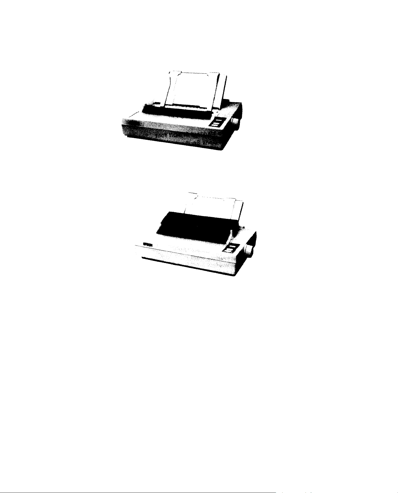
lists the optional units available for the LQ-500/L-1000, and Figure l-l shows an exterior view of the
LQ-500 / L-1000.
Table l-l. Interface Options
NOTE: Refer to the “Optional Interface Technical Manual” for details.
Table 1-2. Optional Units
LQ-500/ L-1000
l-l
Page 10
GENERAL DESCRIPTION
(Printer Cover A)
R
EV .-A
Figure 1-l.
(Printer Cover B)
Exterior View of the LQ-500/L-I000
LQ-500 / L-1000
1-2
Page 11

REV.-A
1.2 SPECIFICATIONS
This section describes the specifications for the LQ-500/L-1000 printer.
1.2.1 Hardware Specifications
GENERAL DESCRIPTION
Printing Method
Pin Configuration
Serial, impact, dot matrix
24 wires (12 x 2 staggered, diameter 0.2 mm)
Feeding Method
Line Spacing
Paper Insertion
Paper-Feed Speed
Paper Specifications
LQ-500/ L-1000
Figure 1-2. Pin Configuration
Friction feed, tractor feed (pull tractor)
1/6 inch, or programmable in units of 1/l80 inch
From rear
100 ms/line (at 1/6-inch feed)
2.2 inches per second (continuous feed)
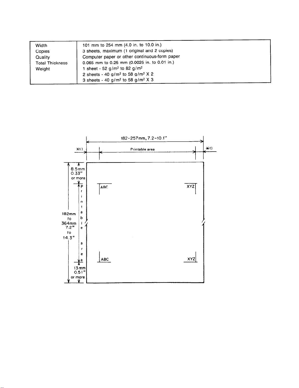
See Tables 1-3 and 1-4
Table 1-3. Cut-Sheet Specifications
1-3
Page 12
GENERAL DESCRIPTION
Table 1-4. Continuous (Sprocket) Paper Specifications
Printable Area
The figure below illustrates the printable area for cut sheets.
REV.-A
*1) 3 mm or more using 182 mm to 229 mm (7.2 in. to 9 in.) width paper.
27 mm or more using 257 mm (10.1 in.) width paper.
Figure 1-3. Cut-Sheet Printable Area
1-4
LQ-500/ L-1000
Page 13
REV.-A
GENERAL DESCRIPTION
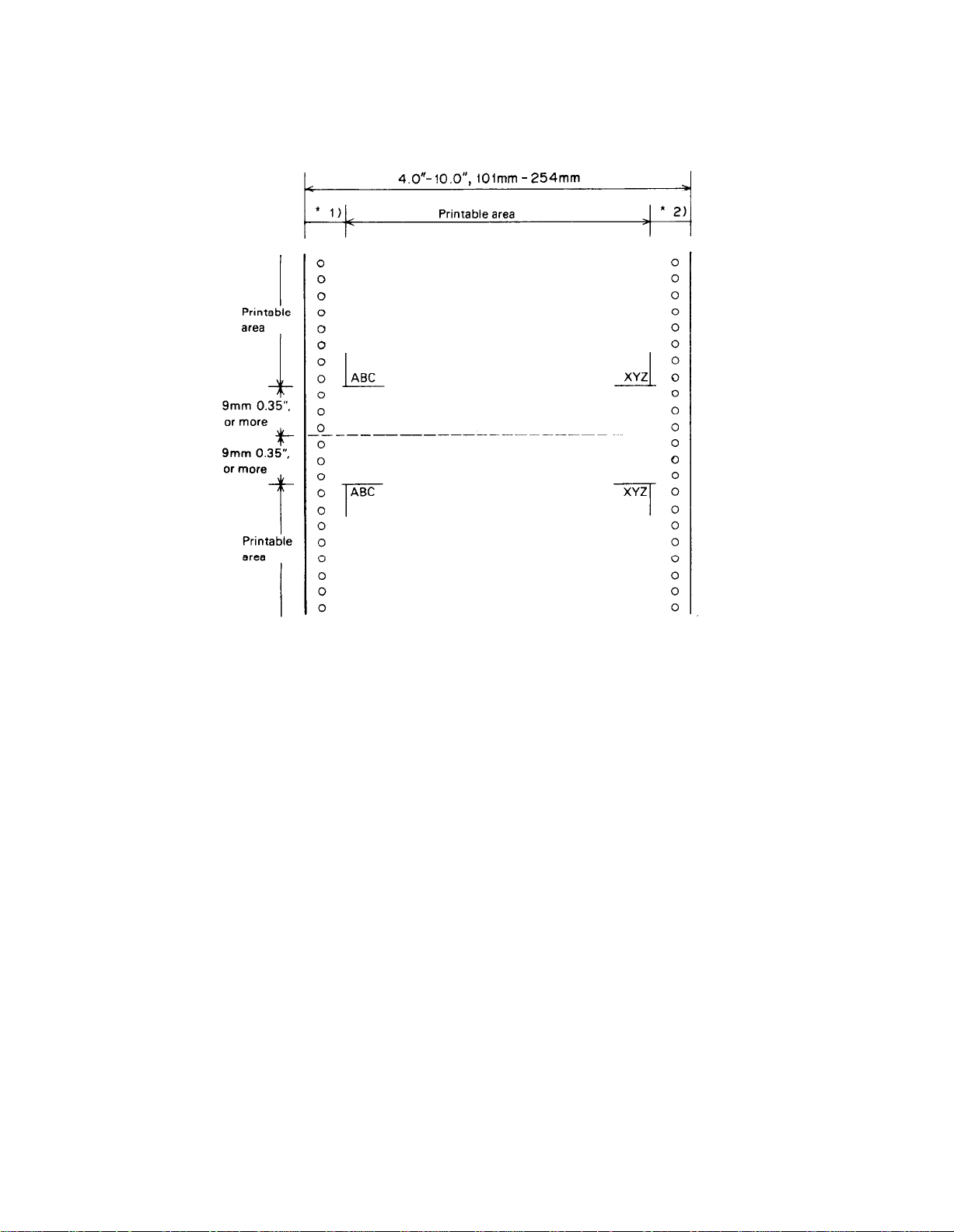
*1) 13 mm or more using 101 mm to 242 mm (4 in. to 9.5 in.) width paper.
26 mm or more using 254 mm (10 in.) width paper.
l 2) 13 mm or more using 101 mm to 242 mm (4 in. to 9.5 in.) width paper.
24 mm or more using 254 mm (10 in.) width paper.
Figure 1-4. Printable Area for Continuous (Sprocket) -Feed Paper
LQ-500/ L-1000
1-5
Page 14

GENERAL DESCRIPTION
Ink Ribbon
Type
Color
Reliability
Dimensions of Ribbon
Cartridge
Reliability
Mean Cycles Between Failures
(MCBF)
Mean Time Between Failures
(MTBF)
REV.-A
Exclusive ribbon cartridge
Black
2 million characters at 48 dots/character
293 mm (width) x 34 mm (height) x 72 mm (depth)
3 million lines (excluding printhead)
4000 POH (25% duty)
Life of Printhead
200 million strokes
Safety Approvals
Safety Standards
UL478 (U.S. version)
CSA22.2#154
VDE0806 (TUV) (European version)
Radio Frequency
Interference (RFI)
FCC class B (U.S. version)
VDE0871 (Self-certification) (European version)
Electrical Specifications
Power Conditions
120 VAC ± 10% (120 V version)
220 VAC ± 10% (220 V version)
240 VAC ± 10% (240 V version)
Frequency Range
49.5 to 50.5 Hz (50 Hz version)
59.5 to 60.5 Hz (60 Hz version)
Rating Current
1.8A (120 V version)
0.9A (220 V version)
0.9A (240 V version)
Insulation Resistance
10 Megohms min. (Between AC Line and Chassis)
Dielectric Strength
(Between AC Line and Chassis) 1250 VAC (rms), 1 minute (120 V version)
3750 VAC (rms), 1 minute (220/240 V version)
Environmental Conditions
Temperature
Humidity
Resistance to Shock
Resistance to Vibration
Physical Specifications
Weight
Dimensions
1-6
5 to 35 degrees C -operating
-30 to 60 degrees C -in shipment container
10 to 80 % RH -operating
5 to 85 % RH -storage
1 G, within 1 ms -operating
2 G, within 1 ms -storage
0.25 G, 55 Hz max. -operating
0.50 G, 55 Hz max. -storage
7 Kg
390 mm (width) x 320 (depth) x 139 mm (height), excluding knobs
and paper guides
LQ-500/ L-1000
Page 15

REV.-A
1.2.2 Firmware Specifications (ESC/P)
GENERAL DESCRIPTION
Control Code
Printing Direction
Input Data Buffer
Character Code
Character Set
Family
Fonts
Printing Mode
Printing Speed
Printing Columns
Character Matrix
Character Size
ESC/PTM level ESC/P-83 (EPSON Standard Code for Printers)
Bidirectional (text)
Bidirectional (bit-image) (when SW 2-6 is ON)
Unidirectional (bit-image) (when SW 2-6 is OFF)
8K bytes (when SW 2-5 is ON)*
1K byte (when SW 2-5 is OFF)
*When DIP SW 2-5 is set on ON, downloading will be ignored.
8 bits
96 ASCII and 13 international character sets
EPSON Roman (Family number: 0)
EPSON Sans Serif (Family number: 1)
EPSON Roman 10, EPSON Roman 12, EPSON Roman 15,
EPSON Roman Proportional;
EPSON Sans Serif 10, EPSON Sans Serif 12,
EPSON Sans Serif 15, EPSON Sans Serif Proportional;
EPSON Draft 10, EPSON Draft 12, EPSON Draft 15.
Selection and mixture of the following modes are allowed, except 15 CPI
Condensed Mode
0 Printing quality (draft/letter quality)
0 Character pitch (10, 12, 15, or proportional)
0 Condensed
0 Double-width
l Double-height
0 Emphasized
0 Double-strike
0
Italic
l Underlined
0 Outline
0 Shadow
See Table 1-5.
See Table 1-5.
See Table 1-6.
See Table 1-6.
LQ-500/ L-1000
1-7
Page 16

GENERAL DESCRIPTION
REV.-A
Table 1-5. Printing Mode
NOTES:
1. “Max.” means the value when characters of the maximum width were printed.
2. “Min.” means the value when characters of the minimum width were printed.
3. “-" means that “LQ” character set is automatically selected when proportional pitch is specified.
1-8
LQ-500/ L-1000
Page 17

REV.-A
GENERAL DESCRIPTION
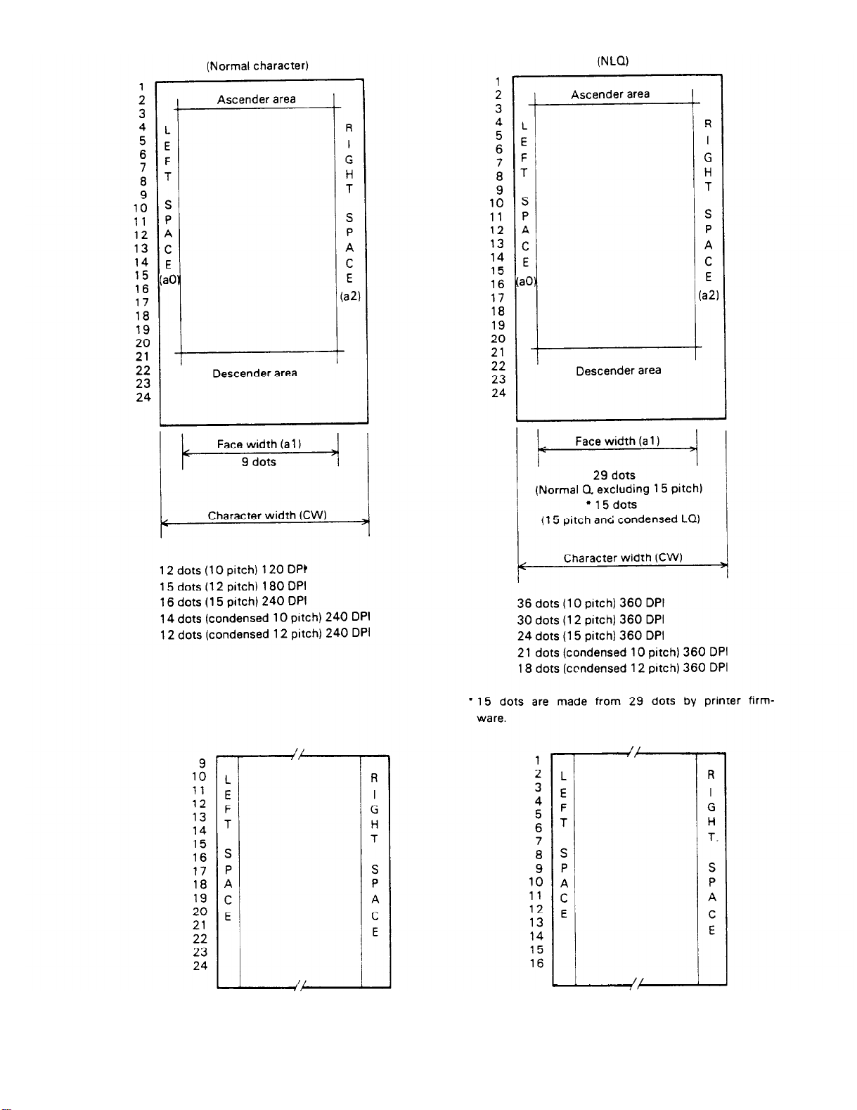
Table 1-6. Character Matrix and Character Size
NOTES:
HDD is horizontal dot density in dots per inch.
1.
Face matrix and character size indicate the size of the maximum character, and this value will be changed
2.
by differences in paper, ribbon, etc.
Unit ESC sp (which also can be sent as the unit followed by the character string CHR$ (&h20)) indicates
3.
the minimum length to be added to the right of the character that can be specified with the ESC sp control
code.
4. 4.""indicates that character matrix is reshaped by printer firmware. Character width becomes half
of noncondensed character width.
LQ-500/L-1000
1-9
Page 18
GENERAL DESCRIPTION
REV.-A
1-10
Figure 1-5. Character Matrix
LQ-500/ L-1000
Page 19

REV.-A
GENERAL DESCRIPTION
1.3 INTERFACE OVERVIEW
The 8-bit parallel interface, provided standard with this printer, has the following specifications:
Data Format
Synchronization
Handshaking
Signal Level
Adaptable Connector
Data Transmission Timing
8-bit parallel
By STROBE pulse
By BUSY and ACKNLG signal
TTL-compatible
57-30360 (Amphenol) or equivalent
See Figure 1-6
Figure 1-6. Data Transmission Timing
Table 1-7 shows the connector pin assignments and signal functions of the 8-bit parallel interface.
Table 1-7. Connector Pin Assignments and Signal Functions
LQ-500 / L-1000
1-11
Page 20

GENERAL DESCRIPTION
Table 1-7. Connector Pin Assignments and Signal Functions (Cont.)
REV.-A
NOTES:
1.
“Dir.” refers to the direction of the signal flow as viewed from the printer.
2.
“Return” denotes a twisted-pair return line.
3. The cable used must be shielded to prevent noise.
4.
All interface conditions are based on TTL levels. Both the rise and fall times of all signals must be less
than 0.2 µs.
5.
The AUTO FEED-XT signal can be set at LOW by DIP switch 2-4.
6.
The SELECT-IN signal can be set at LOW by jumper 6.
7.
Printing tests, including those of the interface circuits, can be performed without using external equipment
by setting DATA 1-8 of the interface connector to certain codes and connecting the ACKNLG signal to the
STROBE signal.
1-12
LQ-500/ L-1000
Page 21
REV.-A
GENERAL DESCRIPTION
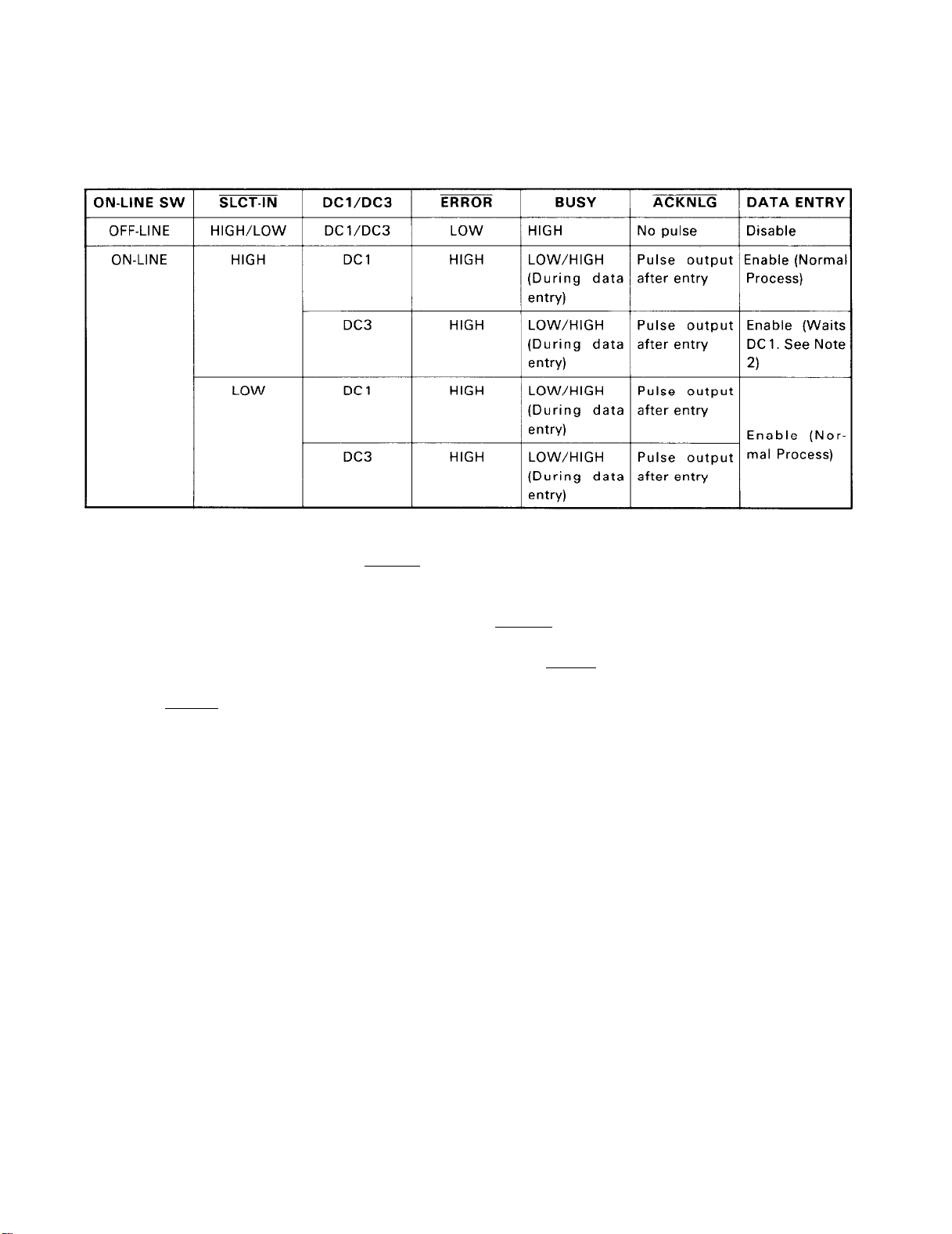
Table 1-8 shows the printer select/deselect (DC1 /DC3) control, including relations among ON-LINE, SELECT-IN
input, DC1 /DC3, and interface signals.
Table 1-8. Printer Select/Deselect Control
NOTES:
1.
In Table 1-8, it is assumed that no ERROR status exists other than that attributable to OFF-LINE mode.
2.
Once the printer is deselected by the DC3 code, the printer will not revert to the selected state unless the
DC1 code is input again. (In the deselected state, the printer ignores input data until the DC1 code is received.)
3.
The DC1 and DC3 codes are enabled only when the SLCT-IN signal (Input Connector 36 for the parallel
interface unit) is HIGH and printer power is initialized.
4.
If the SLCT-IN signal is LOW when the printer is initialized, DC1 /DC3 printer select/deselect control is
invalidated, and these control codes are ignored.
5.
If the SLCT-IN signal is HIGH and is not set to LOW by jumper 6 when printer initialized, the printer
starts from the selected (DCl) state.
LQ-500/ L-1000
1-13
Page 22

GENERAL DESCRIPTION
REV.-A
1.4 DIP SWITCHES AND JUMPER SETTING
This section describes the DIP switch selections and the jumper setting for the LQ-500/L-1000 printer.
1.4.1 DIP Switch Settings
The two DIP switches for the printer are located inside the ROM cartridge slot cover and function as shown
in Tables 1-9 through 1-13. (Note that the status of the DIP switches is read only at power on or upon receipt
of the INIT signal.)
Table 1-9. Settings for DIP Switch 1 (SW1)
* Unidirectional printing is selected by default, however input of ESC U O can be used to set the print direction to
Bidirectional.
Table 1-11. International Character Set Selection
1-14
LQ-500/ L-1000
Page 23

REV.-A
GENERAL DESCRIPTION
Table 1-12. Font Selection
1-4 1-5
Off Off
On
Off On
On On
Off
Font
Roman
Sans Serif
Slot
Draft
Table 1-13. Character Pitch Selection
2-7 2-8
Off
On
Off On
On On
Off
Off
Character Pitch
10 CPI
12 CPI
15 CPI
Proportional
1.4.2 Jumper Setting
Jumper 6, which is user-selectable, is located inside the ROM cartridge slot cover. If the jumper is connected,
the SLCT-IN signal is fixed to LOW, and DC1 /DC3 printer select control is ignored.
1.5 SELECTYPE FUNCTION
Selectype allows the user to choose fonts easily while the printer is ON-LINE. This function provides for selec-
tion of Draft, Roman, Sans Serif, or the slot (ROM cartridge) font. SelecType is effective only when the printer
is ON-LINE and is not printing. Font selection is performed by pressing the FORM-FEED switch with the printer
ON-LINE and not printing. The printer’s control panel indicates which font has been specified.
LQ-500/ L-1000
1-15
Page 24

GENERAL DESCRIPTION
REV.-A
1.6 OPERATING INSTRUCTIONS
This section describes the self-test and hexadecimal dump functions and also includes the error states, printer
initialization, and the buzzer operation.
1.6.1 Self-Test
To begin printing the self-test using Draft mode, turn the printer ON while pressing the LINE-FEED button. To
begin printing the self-test using the Letter Quality (LQ) mode, turn the printer power ON while pressing
FORM-FEED.
Self-test printing can be stopped or started by pressing ON-LINE (ON-LINE indicator is not lit). To finish the
self-test, stop the printing by pressing the ON-LINE switch and turn OFF the printer power.
The firmware revision number is printed as the first line of the self-test, and subsequently, current DIP switch
settings are printed.
1-16
Figure 1-7. Self-Test Printout
LQ-500/ L-1000
Page 25
REV.-A
GENERAL DESCRIPTION
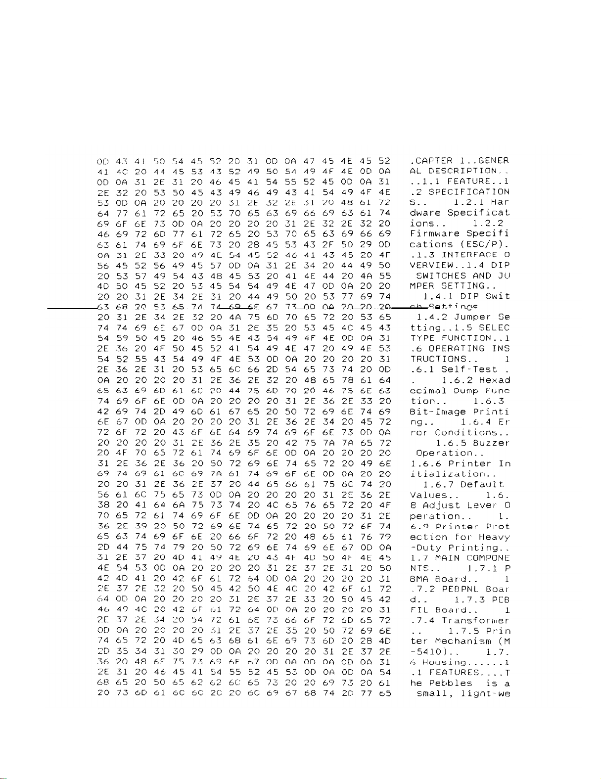
1.6.2 Hexadecimal Dump Function
The printer enters HEX-DUMP mode when it is powered on while the LINE-FEED and FORM-FEED buttons
are pressed down. In HEX-DUMP mode, the hexadecimal representation of the input data is printed out, along
with corresponding ASCII characters. This function is valuable for checking the data the printer has received
from the host. If input data is a control code rather than a character code, a period (.) is printed in the ASCII column.
Data Dump Mode
LQ-500/ L-1000
Figure 1-8. Hexadecimal Dump Function
1-17
Page 26
GENERAL DESCRIPTION
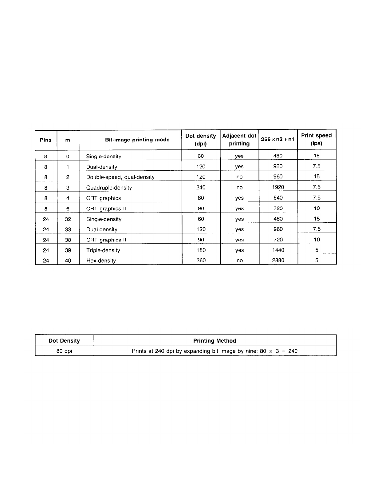
1.6.3 Bit-Image Printing
This printer has four standard print densities, listed below in dots per inch (dpi):
120 dpi (including half dots): Triple speed
180 dpi (including half dots): Double speed
240 dpi (including half dots): 1.5 speed
360 dpi (including half dots): Normal speed
The firmware, however, implements the print densities as shown in Table 1-14
Table 1-14. Print Density
REV.-A
NOTES: ESC* m n1 n2 [DATA] n2 x 256 + n1
dpi = dots per inch
ips = inches per second
The firmware handles the print densities as shown in Table 1-15.
Table 1-15. Bit-Image Printing
1-18
LQ-500/ L-1000
Page 27

REV.-A
GENERAL DESCRIPTION
1.6.4 Error Conditions
If any of the following error conditions is detected, the printer automatically enters OFF-LINE mode.
0 Home position is not detected at printer mechanism initialization.
e Home position is detected during printing.
0 ON-LINE is pressed, and the printer enters OFF-LINE.
l A paper-out signal is detected and forms-override is finished.
0 Paper out is detected after the printer performs a paper-loading operation with the cut-sheet feeder enabled.
The following interface signals are output to indicate the error and to halt data transmission:
BUSY signal becomes HIGH.
ERROR becomes LOW.
No ACKNLG pulse is sent.
1.6.5 Buzzer Operation
The buzzer sounds under the following circumstances:
0 When the BEL code is sent to the printer (0.5-second ring).
0
When a paper-out error is detected, the buzzer sounds 3 times (rings for 0.1 second with a 0.1-second interval).
0 When abnormal carriage movement is detected, the buzzer sounds 5 times (rings for 0.5 second, with a 0.5-
second interval).
l When a panel setting is accepted (0.1-second ring).
1.6.6 Printer Initialization
There are two initialization methods: hardware initialization and software initialization.
Hardware Initialization
This type of initialization takes place when the printer power switch is turned ON (and the AC power cord is
plugged in) or when the INIT signal is received over the parallel interface line.
When the printer is initialized, it performs the following actions:
(a) Initializes printer mechanism.
(b) Clears input data buffer.
(c) Clears downloaded character set.
(d) Clears the print buffer.
(e) Returns printer settings to their default values.
Software Initialization
This type of initialization takes place when the printer receives the software initialize code. Upon receipt of this
code, the printer does not perform the functions listed above under (a), (b), and (c). The settings changed by
the last SelecType operation are reset.
LQ-500/ L-1000
1-19
Page 28

GENERAL DESCRIPTION
1.6.7 Default Values
When the printer is initialized, the following default values or functions are set:
REV.-A
Page Position
Left and Right Margins
Line Spacing
Vertical Tabs
Horizontal Tabs
VFH Channel
Category of Type Style
Current paper position becomes top-of-form position
Released
116 inch
Cleared
Every 8 characters (relative)
Channel 0
SelecType - Software initialization
DIP switch - Hardware initialization
Downloaded Characters
Deselected - Software initialization
Cleared - Hardware initialization
Justification
Character Spacing
Bit-Image Mode Assignment
Left justification
10 CPI
ESC K = ESC + 0, ESC L = ESC * 1
ESC Y = ESC * 2, ESC Z = ESC * 3
Printing Effects
Cleared
1.6.8 Adjust Lever Operation
The head adjust lever must be set to the proper position according to the paper thickness. See Table 1-16
and Figure 1-9.
Table 1-16. Lever Position Operation
1-20
Figure 1-9. Lever Position
LQ-500/ L-1000
Page 29

REV.-A.
GENERAL DESCRIPTION
1.6.9 Printer Protection for Heavy-Duty Printing
This printer has “printhead protection” to safeguard the printhead from overheating or from voltage dropping
to the head driver.
If head temperature exceeds upper limit value, then printing is automatically stopped until head temperature
has dropped to a certain value to resume printing.
If heavy-duty printing causes the voltage supplied to the head drive circuit to drop to the lower limit, then printing is interrupted immediately, and thereafter, if power supply voltage is recovered to a certain value, then the
remaining print line will be printed. This protection will occur when half or more of the wires are activated
simultaneously and continuously.
LQ-500/L-1000
1-21
Page 30

GENERAL DESCRIPTION
REV.-A
1.7 MAIN COMPONENTS
The main components of the LQ-500/L-1000 printer are designed for easy removal and replacement to maintain/repair the printer. The main components are:
1) PBMA board:
2) PEBPNL board:
3) PEBFIL board:
4) Transformer
5) M-5410:
The main control board; the CPU on this board controls all main functions
The control panel board.
The filter circuit board.
The printer mechanism.
Figure 1-10. LQ-500/L-1000 Component Layout
1.7.1 PBMA Board
The use of the µPD7810HG CPU makes the main control board simple in its circuit design.
Figure 1-11. PBMA Main Control Board
1-22
LQ-500/ L-1000
Page 31

REV.-A
GENERAL DESCRIPTION
1.7.2 PEBPNL Board
The PEBPNL board is the LQ-500/L-1000 control panel, which contains the indicator LEDs, switches, and buzzer.
Figure 1-12. PEBPNL Control Panel Board
1.7.3 PEBFIL Board
The PEBFIL board eliminates noise from the AC line to the printer and from the printer to the outer line. The
fuse used on this board prevents overheating.
LQ-500/L-1000
(120 V Version) (220/240 V Version)
Figure 1-13. PEBFIL Filter Board
1-23
Page 32

GENERAL DESCRIPTION
REV.-A
1.7.4 Transformer
This transformer changes the input AC from the filter circuit into 26 VAC and 12 VAC in order to supply the
necessary voltages to the control circuit board.
(120 V Version)
(220 V Version)
(240 V Version)
Figure 1-14. Transformer
1.7.5 Printer Mechanism (M-5410)
The M-5410 printer mechanism was developed expressly for use with LQ-500/L-1000 printer: the components
include a carriage motor, carriage mechanism, paper-feed motor, paper-feed mechanism, ribbon-feed
mechanism, printhead, and sensors.
1-24
Figure 1-15. Model 5410 Printer Mechanism
LQ-500/ L-1000
Page 33

REV.-A
1.7.6 Housing
LQ-500/L-1000 housing consists of the upper and lower cases. The upper case houses the control panel. The
lower case contains the printer mechanism and the main control board. The printer cartridge is easily removable
and can be replaced simply by lifting the upper case.
GENERAL DESCRIPTION
Figure 1-16. Housing
LQ-500/L-1000
1-25
Page 34

REV.-A
CHAPTER 2
PRINCIPLES OF OPERATION
2.1
2.2
OVERVIEW
2.1.1 SummaryofConnectors..
2.1.2 Overview of Printer
2.1.3
2.1.4
PRINCIPLES
2.2.1
2.2.2
2.2.3
2.2.4
2.2.5
2.2.6
.....................................................................................
Mechanism
2.1.2.1
2.1.2.2
2.1.2.3
OverviewofCircuitry.. ........................................................
Firmware Overview
Power Supply Circuit ..........................................................
2.2.1.1
2.2.1.2 Chopper-Type Switching
2.2.1.3
2.2.1.4 Transformer
2.2.1.5 Rectifier and Smoothing
2.2.1.6
2.2.1.7
2.2.1.8 + 24 VDC
2.2.1.9
2.2.1 .10 Vx
Reset Circuit
Firmware OperationatReset..
Address Decorder and
Carriage Operation
2.2.5.1
2.2.5.2
2.2.5.3
2.2.5.4
2.2.5.5
2.2.5.6
Paper Feed
2.2.6.1
2.2.6.2
Sensors.. .............................................................
Motors
Printhead
OF
OPERATION..
Power Supply Circuit Block Diagram
Filter
+ 5
Pulse-Width Modulation
+ 12
Carriage Mechanism
Carriage
Carriage Motor Drive Circuit Block Diagram..
Gate Array EOlA05KA Operation in Carriage
Motor Drive Circuit
Carriage Motor Drive Circuit
Carriage
Paper-Feed Mechanism Operation
Paper-Feed
................................................................
............................................................
.............................................................
.........................................................
Circuit
.........................................................
VDC
Regulator Circuit
Regulator Circuit..
VDC
Supply
Voltage
......................................................................
........................................................................
Supply
.............................................................
Motor Specifications...............................
Motor Software
Motor Specifications..
....................................................
Operation.. ..........................
.....................
Regulator Circuit.. ...........
........................................................
Circuit
(PWM) Circuit..
Circuit.. .....................................
Circuit..
.............................................
Bank
Register..
.............................................
...............................................
Control.. .........................
............................
....................................
.................
.................................
...................................
.................................
.........
.................................
.........................
.........................
2-1
2-1
2-3
2-4
2-6
2-6
2-7
2-8
2-9
2-9
2-9
2-13
2-12
2-12
2-11
2-14
2-16
2-18
2-20
2-21
2-22
2-26
2-30
2-32
2-32
2-32
2-33
2-34
2-36
2-42
2-49
2-49
2-51
LQ-500/L-1000
2-i
Page 35

REV.-A
2.2.7
2.2.8
2.2.9
2.2.10
2.2.11
Circuit
2.2.6.3
2.2.6.4
Printhead
2.2.7.1
2.2.7.2
2.2.7.3
2.2.7.4
2.2.7.5
2.2.7.6
A/D Converter Circuit..
Host
Buffer and Data Flow..
2.2.10.1
2.2.10.2
Ribbon-Feed
Paper-Feed
Paper-Feed
...........................................................................
Printhead Printing Operation
Printhead Specifications
Printhead Drive Circuit Block Diagram..
Gate Array E05A02LA Operation in Printhead
Drive Circuit
Printhead
Printhead
Interface ....................................................................
Buffer
Data Flow..
Mechanism
Motor
Motor Software
Drive
Software
.................................................................
..........................................................
Drive
.......................................
........................................................
Circuit
.......................................................
........................................................
.....................................................
.........................................
Control..
.............................
Control.. .....................
.................................
.................................
.................
2-51
2-52
2-54
2-54
2-55
2-55
2-56
2-58
2-59
2-61
2-64
2-67
2-67
2-70
2-72
FIGURE 2-1.
FIGURE 2-2.
FIGURE 2-3.
FIGURE 2-4.
FIGURE 2-5.
FIGURE 2-6.
FIGURE 2-7.
FIGURE 2-8.
FIGURE 2-9.
FIGURE 2-10.
FIGURE 2-11.
FIGURE 2-12.
FIGURE 2-13.
FIGURE 2-14.
FIGURE 2-15.
FIGURE 2-16.
FIGURE 2-17.
FIGURE 2-18.
FIGURE 2-19.
LIST OF FIGURES
Cable
Printer Mechanism
Paper-End
Thermal Sensor (Printhead Temperature Detection).
Connectors..
Sensor..
Home-Position Sensor
Printhead
Circuit Block Diagram
Memory Map (64K
Power Supply Circuit
Step-Down
Step-Down Timings
PEBFIL Filter Circuit
Transformer Circuit
Rectifier and Smoothing Circuit
+5 V Regulator Circuit
Oscillator
Constant Voltage Control (+ 5 VDC)
AMP
NJM2355 Internal Circuit
........................................................................
Circuit..
Waveform
Output
1
..........................................................
Block Diagram
..........................................................
.....................................................
......................................................
Bytes)
.................................................................
.................................................
Block Diagram..
..........................................................
.........................................................
Board
..........................................................
........................................................
..............................................
....................................................
..................................................
....................................
...............................
........................................
..................................
..........
2-2
2-3
2-4
2-4
2-5
2-6
2-7
2-8
2-9
2-11
2-11
2-12
2-12
2-13
2-14
2-14
2-15
2-15
2-16
2-ii
LQ-500 / L-1 000
Page 36

REV.-A
FIGURE 2-20.
FIGURE 2-21.
FIGURE 2-22.
FIGURE 2-23.
FIGURE 2-24.
FIGURE 2-25.
FIGURE 2-26.
FIGURE 2-27.
FIGURE 2-28.
FIGURE 2-29.
FIGURE 2-30.
FIGURE 2-31.
FIGURE 2-32.
FIGURE 2-33.
FIGURE 2-34.
FIGURE 2-35.
FIGURE 2-36.
FIGURE 2-37.
FIGURE 2-38.
FIGURE 2-39.
FIGURE 2-40.
FIGURE 2-41.
FIGURE 2-42.
FIGURE 2-43.
FIGURE 2-44.
FIGURE 2-45.
FIGURE 2-46.
FIGURE 2-47.
FIGURE 2-48.
FIGURE 2-49.
FIGURE 2-50.
FIGURE 2-51.
FIGURE 2-52.
FIGURE 2-53.
FIGURE 2-54.
FIGURE 2-55.
FIGURE 2-56.
FIGURE 2-57.
Output Transistor Drive Waveform
+24 V Regulator Circuit
Constant-Voltage Control (+ 24 VDC)
Over-Current Protection (OCP)
+ 12 VDC Circuit
Vx Voltage Circuit
Reset Circuit
RESET Output
RESET Pulse Oscillation Process (Module Mounted) ..........
RESET Pulse Oscillation Process (Module Removed) .........
Initialization
Memory
Carriage Mechanism
Carriage Drive Circuit Block Diagram
Gate Array Operation
Carriage Motor Drive
STK-6981 B Circuit Diagram
Reference
Constant Current Control
Chopping
Schmitt
Chopping
Carriage Motor
Home-Position
Printing
Friction-Feed Operation
Sprocket-Feed Operation.. ................................................
Paper-Feed Motor Drive
Paper-Feed Motor
Printhead Printing Operation
Printhead Drive Circuit Block Diagram
E05A02LA
Printhead Drive Circuit
Printhead Driving
Print
Relationship between Head Driver Voltage and Print
Driving Pulse
A/D
Host
Map
Voltage
Waveforms.. .....................................................
Trigger Circuit.. ...................................................
Current and
Area and
Block
Timing.. ..................................................................
Converter Circuit
Interface .................................................................
.............................................................
...................................................................
.................................................................
Program
...................................................................
Control.. ...................................................
Seek.. .......................................................
Diagram.. ...............................................
Width.. .......................................................
...................................................
............................................................
Flowchart.. ......................................
........................................................
.......................................................
Circuit.............................................
..............................................
Generation Circuit
Circuit..
Drive
Printing
Drive Timing
Waveforms
Timing.....................................
...................................................
Circuit..
.....................................................
......................................................
....................................
................................
..........................................
................................
...............................
.....................................
Speed.. .................................
.......................................
Chart
...............................
............................................
..............................
...........................................
2-17
2-18
2-19
2-19
2-20
2-21
2-22
2-23
2-24
2-25
2-26
2-29
2-31
2-32
2-33
2-35
2-36
2-37
2-38
2-39
2-40
2-42
2-43
2-47
2-48
2-49
2-50
2-51
2-52
2-54
2-55
2-56
2-58
2-58
2-59
2-59
2-60
2-62
LQ-500/L-1000
2-iii
Page 37

REV.-A
FIGURE 2-58.
FIGURE 2-59.
FIGURE 2-60.
FIGURE 2-61.
FIGURE 2-62.
FIGURE 2-63.
FIGURE 2-64.
FIGURE 2-65.
TABLE 2-1.
TABLE 2-2.
TABLE 2-3.
TABLE 2-4.
TABLE 2-5.
TABLE 2-6.
TABLE 2-7.
TABLE 2-8.
TABLE 2-9.
TABLE 2-10.
TABLE 2-11.
TABLE 2-12.
TABLE 2-13.
TABLE 2-14.
TABLE 2-15.
TABLE 2-16.
TABLE 2-17.
TABLE 2-18.
TABLE 2-19.
TABLE 2-20.
TABLE 2-21.
Buffer
Input
Line Buffer Structure
Image Buffer Structure
Queue
Download
Routine.. .................................................................
Main
Printing
Ribbon-Feed
Buffer
Buffer
Routine
Structure..
Structure..
..............................................................
Mechanism
....................................................
.......................................................
.....................................................
..................................................
Structure..
.............................................
..................................................
LIST OF TABLES
Board
Power
Control
Control
Reference
Current
Phase-Excitation
Drive
Drive
Chopping
Time
Acceleration Time Data (2-2 Excitation)
Deceleration
Acceleration
Deceleration
Excitation Sequence (Clockwise: Paper Feeds Forward).
Setting
E05A02LA
Scan
Control
Ribbon-Feed
Connector Summary
Supply Applications
Commands..
Commands..
Voltage ...........................................................
Values for
Sequence
Sequence
Current............................................................
Constants
Time Data (2-2
Time Data (1-2
Time Data (1-2
Time
...................................................................
Gate
Lines
and
Commands..........................................................
Gear Train
........................................................
........................................................
Reference
Method..
Excitation).
(2-2
Excitation). .......................................
(1-2
Speeds.. ............................................
for
Array
Switches..
DIP
..............................................
...............................................
Voltages..
................................................
.......................................
Excitation). ............................
Excitation). ............................
Excitation). ............................
Functions.. .....................................
.........................................
...................................................
............................
.............................
....
2-65
2-65
2-66
2-66
2-67
2-68
2-69
2-70
2-1
2-10
2-30
2-34
2-37
2-39
2-41
2-41
2-42
2-43
2-43
2-44
2-44
2-45
2-46
2-52
2-53
2-57
2-61
2-63
2-70
2-iv
LQ-500/ L-1000
Page 38

REV.-A
PRINCIPLES OF OPERATION
2.1 OVERVIEW
This chapter describes the signals at the various connectors that link the primary Components of the
LQ-500/L-1000, including the printer mechanism, power supply circuits, and control circuits. The chapter also
describes the operation of the printer’s circuitry and printer mechanism.
2.1.1 Summary of Connectors
The interconnection of the primary components is shown in Figure 2-1. Table 2-l summarizes the function,
size, and type of the connectors designated in the figure.
Table 2-1. Board Connector Summary
LQ-500/L-1000
2-l
Page 39

PRINCIPLES OF OPERATION
REV.-A
2-2
Figure 2-1. Cable Connections
LQ-500/L-1000
Page 40

REV.-A
2.1.2 Overview of Printer Mechanism Operation
The Model 5410 printer mechanism is a serial, impact, dot-matrix printer that prints at 180 dots per inch (DPI)
in both the horizontal and vertical directions. Figure 2-2 shows a block diagram of the Model 5410 printer
mechanism.
PRINCIPLES OF OPERATION
Figure 2-2. Printer Mechanism Block Diagram
LQ-500 / L-1000 2-3
Page 41

PRINCIPLES OF OPERATION
2.1.2.1 Sensors
The printer mechanism is equipped with the following sensors:
Paper-End (PE) Sensor
Home-Position (HP) Sensor
Thermal Sensor (Printhead Temperature)
Paper-End Sensor (PE Sensor)
Figure 2-3 shows the paper-end sensor. This sensor switch is ON when paper runs out.
Paper-out state - ON + LOW level
Paper present - OFF - HIGH level
REV.-A
Figure 2-3. Paper-End Sensor
Home-Position Sensor (HP Sensor)
Figure 2-4 shows the home-position sensor. This sensor switch is ON when the carriage is at the home position.
Home position - ON + LOW level
Other position - OFF + HIGH level
The reference position for the carriage driver is determined by this sensor.
2-4
Figure 2-4. Home-Position Sensor
LQ-500/ L-1000
Page 42

REV.-A
Thermal Sensor (Printhead Temperature Detection)
The thermal sensor in the printhead monitors printhead temperature. If head temperature exceeds the upper
limit value, then printing is automatically stopped until head temperature drops to a certain value before resuming printing.
Figure 2-5 below illustrates the printer’s thermal-sensor circuit.
PRINCIPLES OF OPERATION
Figure 2-5. Thermal Sensor (Printhead Temperature Detection)
LQ-500 / L-1000
2-5
Page 43

PRINCIPLES OF OPERATION
REV.-A
2.1.2.2 Motors
This printer has the following motors:
Carriage motor (stepper motor)
Paper-feed motor (stepper motor)
Carriage Motor
The carriage motor is used to move the carriage right and left along the platen. This unit employs a 4-phase,
48-step motor using either 1-2 or 2-2 phase excitation and is controlled by an open-loop system.
Paper-Feed Motor
Paper feeding is carried out by a 4-phase, 48-step motor. This unit is designed to advance the paper l/180
inch for each step (phase switch), using 2-2 phase excitation. The motor is controlled by the CPU in an openloop configuration.
2.1.2.3 Printhead
Figure 2-6 shows the dot-wire operation. The head-driving coil is energized, so that the dot wire is pushed out.
The dot wire strikes the ribbon against the paper, printing a dot.
2-6
Figure 2-6. Printhead
LQ-500/L-1000
Page 44

Page 45

PRINCIPLES OF OPERATION
2.1.4 Firmware Overview
This printer has a µPD7810HG CPU with 64K bytes of address space. Figure 2-8 shows a memory map of this
address space.
REV.-A
NOTE: CG = character generator.
GA = gate array.
2-8
Figure 2-8. Memory Map (64K Bytes)
LQ-500/ L-1000
Page 46

REV.-A
PRINCIPLES OF OPERATION
2.2 PRINCIPLES OF OPERATION
This section describes the operation of each component.
2.2.1 Power Supply Circuit The paragraphs below provide details of power supply circuit operations.
2.2.1.1 Power Supply Circuit Block Diagram
120/220/240 VAC are applied to the step-down transformer via the filter circuit to create 26 VAC and 12 VAC,
which are then input to the power supply circuit on the main board. The 26 VAC are converted into about 36
VDC via the full-wave rectifier and smoothing circuit, and input to the regulator circuits for + 24 VDC and + 5
VDC to be supplied to the control circuit. The + 24 VDC and + 5 VDC are also supplied to the Vx voltage circuit
and, while generating the Vx voltage, transferred to the control circuit.
The 12 VAC supplies a nonstabilized + 12 V to the control circuit via the positive terminal of the half-wave rec-
tifier and smoothing circuit.
LQ-500/ L-1000
Figure 2-9. Power Supply Circuit Block Diagram
2-9
Page 47

PRINCIPLES OF OPERATION
REV.-A
Table 2-2. Power Supply Applications
2-10
LQ-500 / L- 1000
Page 48

REV.-A
PRINCIPLES OF OPERATION
2.2.1.2 Chopper-Type Switching Regulator Circuit
A chopper-type switching regulator is employed in the power supply circuit. Operation of the step-down circuit
is as follows:
Figure 2-10. Step-Down Circuit
Figure 2-10 shows the chopper-type, step-down switching regulator circuit. When the transistor is ON, voltage
Vi is applied to coil L and capacitor C, and load current IL flows. At this time, electromagnetic energy WL is
accumulated in choke coil L. When the transistor turns off, energy WL is applied to the load via flywheel diode
D so that output voltage Vo becomes the average value:
LQ-500/L-1000
Figure 2-11. Step-Down Timings
2-11
Page 49

PRINCIPLES OF OPERATION
REV.-A
2.2.1.3 Filter Circuit
The AC line voltage passes through the power switch, then is input to the filter circuit. A fuse, F1, is used on
the PEBFIL board. The filter circuit attenuates external noise and inhibits noise generated in the printer from
going out via the AC line. Either Cl or C2 drains leakage current between the primary coil and the case. Figure
2-12 shows the filter circuit.
Figure 2-12. PEBFIL Filter Circuit Board
2.2.1.4 Transformer
AC voltages (120 VAC, 220 VAC, 240 VAC) that pass through the filter circuit are divided into 26 VAC and
12 VAC and supplied to the PBMA circuit. Figure 2-13 shows a schematic drawing of the power transformer.
Figure 2-13. Transformer Circuit
2-12
LQ-500/ L-1000
Page 50

REV.-A
2.2.1.5 Rectifier and Smoothing Circuit
The 26 VAC from the secondary coil of the transformer are full-wave rectified by diode bridge DB1, and converted to approximately 36 VDC by smoothing capacitor C40. The + 24 VDC and + 5 VDC voltages are converted from this DC voltage, which is used as the power supply voltage for the switching regulator IC at the
next stage.
PRINCIPLES OF OPERATION
Figure 2-14. Rectifier and Smoothing Circuit
LQ-5001 L-1000
2-13
Page 51

PRINCIPLES OF OPERATION
REV.-A
2.2.1.6 + 5 V Regulator Circuit
Figure 2-15 shows the +5 VDC regulator circuit. An NJM2355 switching regulator IC is used for constant-
frequency pulse-width modulation. The circuit shown above employs an NJM2355 configured as a chopper-
style switching regulator circuit.
This IC has a built-in oscillator. The oscillation frequency is determined by external components connected
to pins 2 and 3. Therefore, R105 and C34 cause the circuit to oscillate at about 30 KHz. The oscillator waveform
is shown in Figure 2-16.
2-14
Figure 2-15. + 5 V Regulator Circuit
Figure 2-16. Oscillator Waveform
LQ-500 / L- 1000
Page 52

REV.-A
PRINCIPLES OF OPERATION
AMP 1 in the IC is an error amplifier used to monitor the output voltage. Figure 2-17 shows the constant-voltage
control circuit. Pin 1 of the IC provides a 5 V reference output (Vref), which is applied to the negative terminal
of AMP 1. The error amplifier adjusts its output according to the voltages applied to the positive and negative
input terminals. This has the effect of maintaining the voltage at the positive terminal at 5 V.
Figure 2-18 shows the output from AMP 1. When the voltage at pin 4 becomes higher than that at pin 5 (over
voltage), AMP 1 outputs current modulated by pulse-width modulation (PWM) to reduce the output voltage of
the circuit. PWM is described below.
Figure 2-17. Constant Voltage
Figure 2-18. AMP 1 Output
Control (+ 5 VDC)
R108 and C35 compensate for phase lag in the error amplifier to prevent abnormal oscillation.
LQ-500/ L-1000
2-15
Page 53

PRINCIPLES OF OPERATION
REV.-A
2.2.1.7 Pulse-Width Modulation (PWM) Circuit
Figure 2-19 shows the internal circuit of the NJM2355 IC. The PWM comparator operates as follows:
In circuit 1 the output from AMP 1 flows into the negative terminal of comparator 1, and the outputs from AMP
2 and AMP 3 in circuit 2 flow into the negative terminal of PWM comparator 2 without wired OR. Dead-time
control voltage is also input to additional negative terminals of both PWM comparators 1 and 2.
A sawtooth waveform from the oscillator is input to the positive terminals. The sawtooth waveform from the
oscillator causes the comparators to generate pulses as shown in Figure 2-20.
2-16
Figure 2-19. NJM2355 Internal Circuit
LQ-500/ L-1000
Page 54

REV.-A
As shown in Figure 2-20, when the potential at the NJM2355 is lower than the preset voltage or current value,
it is controlled by the dead-time control voltage. When it exceeds the preset value, it is controlled by the error
amplifier to keep it lower than the preset value.
PRINCIPLES OF OPERATION
Figure 2-20. Output Transistor Drive Waveform
LQ-5001 L-1000
2-17
Page 55

PRINCIPLES OF OPERATION
2.2.1.8 + 24 VDC Regulator Circuit
Figure 2-21 shows the + 24 V regulator circuit. The + 24 VDC regulator circuit has almost the same function
and employs the same oscillation circuit as the +5 VDC regulator circuit. Here, the error amplifier AMP 2 is
used for over-current control, and AMP 3 for constant-voltage control. The operation of the error amplifier AMP
REV.-A
Figure 2-21. +24 V Regulator Circuit
2-18
LQ-500/ L-1000
Page 56

REV.-A
PRINCIPLES OF OPERATION
The negative terminal of AMP 3 receives VREF (5 V). Consequently, the voltage applied to the positive terminal
is adjusted to 5 V. Therefore, based on Figure 2-22, the output voltage is set to the following value:
Figure 2-22. Constant-Voltage Control (+ 24 VDC)
AMP 2 operates as follows for over-current control: + 24 V is applied to the negative terminal, and the positive
terminal will receive an equal voltage when, based on Figure 2-23, a negative current of the following value flows.
Figure 2-23. Over-Current Protection (OCP)
Dead-time control has no bearing in this case, because pin 3 of IC1 is grounded.
LQ-500/ L-1000
2-19
Page 57

PRINCIPLES OF OPERATION
2.2.1.9 + 12 VDC Supply Circuit
The 12 VAC from the transformer is half-wave rectified by diode D19 and is converted to + 12 VDC. As shown
by Figure 2-24, the half-wave rectified voltages pass through the capacitor smoothing circuit so that the ripple
is small, and the average DC voltage rises when no load current flows and drops as load current increases.
Figure 2-24. + 12 VDC Circuit
REV.-A
2-20
LQ-500/ L-1000
Page 58

REV.-A
PRINCIPLES OF OPERATION
2.2.1.10 Vx Voltage Supply Circuit
When the +24 V power supply line reaches 18.6 V (18 V + 0.6 V), transistors Q25 and Q26 turn on and Vx
( + 5 V) is output. On the other hand, if the + 24 V power supply line drops to 18.6 V or less, Q25 and Q26
turn off and the Vx voltage is shut off.
The Vx voltage is used to prevent abnormal operation of the printer when the power is switched on or off.
0 Reset Circuit Power Supply
When the power is switched on or off, the circuit is reset so that it will not drive the printer until the power
supply becomes stable.
0
Pull-ups for the Printhead Signal Lines
These prevent printhead malfunctions when power is switched on or off.
0 Pull-ups for the Paper-Feed Motor Signal Lines
These prevent paper-feed motor malfunctions when power is switched on or off.
LQ-500/ L-1000
Figure 2-25. Vx Voltage Circuit
2-21
Page 59

PRINCIPLES OF OPERATION
REV.-A
2.2.2 Reset Circuit
Figure 2-26 shows the reset circuit. The RESET signal generated here is sent to the RESET terminal of CPU
µPD781 OHG (46) and to connector CN2-13 (optional interface) as a hardware initialization signal. The RESET
signal is output from the circuit when any of the following occurs:
0 Power is turned on or off.
0 The INIT signal is input from either the host interface or an optional interface.
l A module (font or identity) is mounted or removed.
Figure 2-26. Reset Circuit
Power On or Off
D14, R69, and C26 in Figure 2-26 comprise an ON/OFF reset circuit. The purpose of this circuit is to make
the CPU start from address 0000 hex. when power is applied and prevent CPU malfunctions when the power
is switched off.
2-22
LQ-500/ L-1000
Page 60

REV.-A
PRINCIPLES OF OPERATION
The rising edge of the Vx voltage cancels the RESET signal after a delay of time constant T = R69 x C26
produced by the integration circuit of resistor R69 and capacitor C26. The falling
edge of the Vx voltage ac-
tivates a RESET signal by discharging capacitor C26 via diode D14.
The gate array (pins 49 to 51) is used for waveform shaping.
Figure 2-27. RESET Output
INIT Signal Input (from CN1 or CN2)
The external INIT signal (50 µsec or less) is passed through the low-pass filter of R31 and C22, and waveformshaped in the gate array (pin 47 of IC6C) to set the DISC terminal LOW, discharge capacitor C26, and set the
gate array THLD terminal LOW. Following this, the ROUT terminal outputs the RESET signal.
LQ-500/ L-1000
2-23
Page 61

PRINCIPLES OF OPERATION
REV.-A
Module Installation or Removal
Figure 2-28 shows the RESET pulse generation process that occurs when a ROM cartridge is mounted. Numbers
in parentheses below correspond to circled numbers in the figure. After the ROM cartridge is mounted, the
LOW signal flows into the CAR terminal of the gate array (6C), and a LOW signal is correspondingly output
from the DISC terminal and RESET is output from the ROUT terminal.
As the DISC terminal goes LOW, capacitor C26 is discharged with a time constant = R70 x C26. When
the discharge of C26 reduces the potential at the THLD terminal to threshold voltage Vth, the RESET signal
is canceled, and the DISC terminal goes HIGH. After the DISC terminal goes HIGH, Vx voltage
discharges C31 at time constant = R69 x C26 again.
2-24
Figure 2-28. RESET Pulse Oscillation Process (Module Mounted)
LQ-500/L-1000
Page 62

REV.-A
When the ROM cartridge is removed (see Figure 2-29), the CAR terminal of the gate array (6C) receives a HIGH
signal. Then the DISC terminal outputs a LOW signal, and the ROUT terminal outputs a RESET signal.
The remainder of the sequence is similar to that when a ROM cartridge is mounted, so please refer to the
preceding page.
PRINCIPLES OF OPERATION
LQ-500/ L-1000
Figure 2-29. RESET Pulse Oscillation Process (Module Removed)
2-25
Page 63

PRINCIPLES OF OPERATION
2.2.3 Firmware Operation at Reset
After being reset, the CPU executes the initialization program from address 0000 hex. When this program has
completed normally, the CPU enters the standby state and waits for data. Figure 2-30 shows the initialization
program flowchart.
REV.-A
2-26
Figure 2-30. Initialization Program Flowchart
LQ-500/ L-1000
Page 64

REV.-A
PRINCIPLES OF OPERATION
LQ-500/L-1000
Figure 2-30. Initialization Program Flowchart (Cont.)
2-27
Page 65

PRINCIPLES OF OPERATION
REV.-A
2-28
Figure 2-30. Initialization Program Flowchart (Cont.)
LQ-500I L-1000
Page 66

REV.-A
PRINCIPLES OF OPERATION
2.2.4 Address Decoder and Bank Register
This section describes the address decoder and bank register.
Address Decoder
This unit includes an address decoder in gate array E01A05KA (6C). The address decoder outputs a chip-select
signal to the internal PROM (3C), external PROM, 4MCG (5C), 1 MCG (2C), external CG, RAM (2C), HEAD gate
array (7A) via address lines AB12 through AB15 and bank lines 7 and 6 (in the gate array). However, the chip
select for the CS is generated in conjunction with the RD signal, and that of the RAM is generated in conjunction
with the ALE signal.
Software control of firmware can check whether an external PROM is mounted or not, and if the correct PROM
is mounted, the memory map shown in Figure 2-31 is obtained by writing bit 7 LOW at address FOOl hex.
LQ-500I L-1000
Figure 2-31. Memory Map
2-29
Page 67

PRINCIPLES OF OPERATION
Bank Register
This unit has a bank register in gate array EOlA05KA (6C). The bank lines are set by writing to address FO02
hex., and they can be checked by reading the same address.
bits and bank lines.
Table 2-3. Control Commands
Table 2-3 shows the relationship between data
REV.-A
2-30
LQ-500/ L-1000
Page 68

REV.-A
2.2.5 Carriage Operation
This section describes the carriage.
2.2.5.1 Carriage Mechanism
The carriage mechanism includes the printhead, the carriage, the timing belt, the carriage motor, and the platen.
Figure 2-32 shows the carriage mechanism.
The timing belt is connected into the bottom of the carriage. This belt is driven by the carriage motor and moved
via the belt-driven pulley. The printhead is mounted on the carriage, and the entire unit is moved right and
left along the carriage guide shaft and plate.
PRINCIPLES OF OPERATION
Figure 2-32. Carriage Mechanism
2.2.5.2 Carriage Motor Specifications
Carriage motor specifications are as follows:
Type
Drive Voltage
Coil Resistance
Current
LQ-500/ L-1000
4-phase, 48-pole stepper motor
24 V f 10%
21 ohms f 7% at 25 degrees C
Maximum 0.34 A (rush current)
Driving: 0.3 A (typical) (triple speed, 24 V)
0.23 A (typical) (double speed, 1.5 speed, normal speed, 24 V)
Holding: 0.17 A f 20%
2-31
Page 69

PRINCIPLES OF OPERATION
2.2.5.3 Carriage Drive Circuit Block Diagram
REV.-A
Figure 2-33 shows a block diagram of the carriage motor drive circuit.
the carriage motor is not directly executed by the CPU, but by the gate array (6C) using pulses from the CPU.
STK-6981 B is employed to drive the carriage motor using a stabilized current.
Figure 2-33. Carriage Drive Circuit Block Diagram
In this circuit, the phase switching for
2-32
LQ-500/ L-1000
Page 70

REV.-A
2.2.5.4 Gate Array EOlA05KA Operation in Carriage Motor Drive Circuit
The phase switching for the carriage motor (stepper motor) is performed by gate array EOlA05KA (6C). This
gate array first sets the excitation system (2-2 phase or 1-2 phase) and rotation direction (clockwise Or
counterclockwise). Then, after the CPU outputs a pulse to the TM terminal of the gate array, executes auto
phase switching to drive the stepper motor. Figure 2-34 shows this process.
PRINCIPLES OF OPERATION
LQ-500 / L-1000
Figure 2-34. Gate Array Operation
2-33
Page 71

PRINCIPLES OF OPERATION
The carriage motor control port of the gate array is assigned to address FO03 hex. Control commands for the
carriage motor (via the gate array) are listed in Table 2-4.
Table 2-4. Control Commands
When power is turned on
REV.-A
(CW = clockwise; CCW = counterclockwise)
2-34
LQ-500/ L-1000
Page 72

REV.-A
PRINCIPLES OF OPERATION
2.2.5.5 Carriage Motor Drive Circuit
The LQ-500 employs the STK-69816, which is a hybrid IC used to drive stepper motors. STK-6981B (IC8C)
drives the stepper motor with a constant current. The value of the current is determined by an external voltage
level. The IC operation can be separated into phases AB and CD, which are completely equivalent. Phase CD
is described here as a model. Figure 2-35 shows the carriage motor drive circuit. Figure 2-36 shows the
STK-6981 B circuit diagram
LQ-5001 L-1000
Figure 2-35. Carriage Motor Drive Circuit
2-35
Page 73

PRINCIPLES OF OPERATION
REV.-A
NOTE: Phase AB is equivalent to the above.
Figure 2-36. STK-6981 B Circuit Diagram
2-36
LQ-500/ L-1000
Page 74

REV.-A
Reference Voltage Generation Circuit
Figure 2-37 shows the reference voltage generation circuit and Table 2-5 shows the reference voltage.
PRINCIPLES OF OPERATION
Figure 2-37. Reference Voltage Generation Circuit
Table 2-5. Reference Voltage
LQ-500/ L-1000
2-37
Page 75

PRINCIPLES OF OPERATION
REV.-A
Constant Current Drive Circuit
The carriage motor-drive current is given by the following equation:
I = VrCD/R79 = VrCD/1.2 ohms
When the carriage stops, port PB5 of the CPU is set HIGH, the input to the chopping circuit becomes 0 V,
and current is applied from the + 5 V line to the motor via resistor R1 and diode D1. This current is given by:
I =
(5 V - VD15 - VD5)
R76 - 21 ohms/phase + R79
Figure 2-38 shows the constant current circuit; Table 2-6 lists the current values for reference voltages.
2-38
Figure 2-38. Constant Current Control Circuit
LQ-500 / L-1000
Page 76

REV.-A
PRINCIPLES OF OPERATION
Table 2-6. Current Values for Reference Voltages
With positive feedback through R9, a hysteresis, whose upper bound is the reference voltage, is generated
in the comparator of ICl. The comparator works as a Schmitt trigger, which senses a difference only when
the feedback (inverse terminal) is slightly larger or smaller than the hysteresis level. Reference voltage-a and
the feedback voltage are compared by the comparator in IC1. If reference voltage-a is HIGH, TR6 turns on,
applying approximately 25 VDC to the coil. The current rises linearly due to inductance, and TR6 turns off when
the feedback voltage reaches reference voltage. In this manner an almost constant current can be applied to
the coil.
Figure 2-39 shows the drive current waveform (pin 12) of the carriage motor and the chopping waveform (pin
17) of the drive voltage (+ 25 V), at 900 PPS. Figure 2-39 shows the Schmitt trigger circuit.
Figure 2-39. Chopping
Waveforms
LQ-500/ L-1000
2-39
Page 77

PRINCIPLES OF OPERATION
REV.-A
Figure 2-40. Schmitt Trigger Circuit
2-40
LQ-500/L-1000
Page 78

REV.-A
PRINCIPLES OF OPERATION
2.2.5.6 Carriage Motor Software Control
This section describes the carriage motor software control.
Excitation System
The excitation system is determined by the firmware and is executed in accordance with the carriage speed,
as shown in Table 2-7. The motor drive sequence for each excitation system is shown in Tables 2-8 and 2-9.
Table 2-7. Phase-Excitation Method
Table 2-8. Drive Sequence (2-2 Excitation)
LQ-500/ L-1000
2-41
Page 79

PRINCIPLES OF OPERATION
REV.-A
Table 2-9. Drive Sequence (1-2 Excitation)
Since a stepper motor is used for the carriage motor, it is possible to hold at any position and switch printing
direction. The carriage motor control system is an open-loop system which switches the phases in accordance
with set speeds.
The drive chopping current is switched at the drive frequency for the carriage motor. The relationship between
drive speed and switching current value is shown in Figure 2-41, and values for the drive chopping current
are listed in Table 2-10.
2-42
Figure 2-41. Chopping Current and Drive Speed
LQ-500/L-1000
Page 80

REV.-A
Table 2-10. Chopping Current
The times for constant speed, acceleration control, and deceleration control are shown below. The a marks
in the acceleration and deceleration columns control items in the tables and indicate switching times from Al
to A2 or 62 to B1.
PRINCIPLES OF OPERATION
Figure 2-42. Carriage Motor Control
Table 2-11. Time Constants for Speeds
LQ-500/L-1000
2-43
Page 81

PRINCIPLES OF OPERATION
Table 2-12. Acceleration Time Data (2-2 Excitation)
REV.-A
Table 2-13. Deceleration Time Data (2-2 Excitation)
2-44
LQ-500/ L-1000
Page 82

REV.-A
PRINCIPLES OF OPERATION
Table 2-14. Acceleration Time Data (1-2 Excitation)
LQ-500/L-1000
2-45
Page 83

PRINCIPLES OF OPERATION
Table 2-15. Deceleration Time Data (1-2 Excitation)
REV.-A
2-46
LQ-500/L-1000
Page 84

REV.-A
PRINCIPLES OF OPERATION
Home-Position Seek
The control that causes the carriage to move to the home position when the power is turned on is called home-
position seek. Figure 2-43 shows the home-position seek operation. After power is applied, the printer executes
2-2 phase excitation for 20 or 30 ms and checks the HOME signal, regardless of the phase switching timing.
The result of this check determines whether the starting position should be 1 or 2. The carriage enters the
home position only once during the initialization.
LQ-5001 L-1000
Figure 2-43. Home-Position Seek
2-47
Page 85

PRINCIPLES OF OPERATION
Printing Area
The printing area is defined as starting 22 phase switching times after the home position.
REV.-A
Figure 2-44. Printing Area and Printing Timing
Abnormal Carriage Operation
This unit does not employ a print timing signal (PTS) sensor and cannot detect abnormal carriage operation.
Therefore, no error occurs even if carriage movement is prevented by external forces. An error will only occur
if the HOME signal is received in the printing area, in which case the carriage will stop.
2-48
LQ-500 / L-1000
Page 86

REV.-A
PRINCIPLES OF OPERATION
2.2.6 Paper Feed
This section describes the paper-feed operation.
2.2.6.1 Paper-Feed Mechanism Operation
The paper-feed mechanism operates by friction feed for cut sheets and by the sprocket-feed method for fanfold
paper.
Friction-Feed Operation
The paper is held against the platen by two paper-feed rollers and by the printer cover. At this time, the paperfeed motor is driven to rotate the platen gear, via the paper-feed reduction gear, in the direction shown in Figure
2-45. The rotation of the platen gear feeds the paper in the direction of the arrow, due to friction from the paperfeed rollers and platen. Because the paper is held against the platen by the spring force of the paper-feed rollers,
the paper can be released by shifting the paper-release lever forward.
LQ-500/L-1000
Figure 2-45. Friction-Feed Operation
2-49
Page 87

PRINCIPLES OF OPERATION
REV.-A
Sprocket-Feed Operation
When using the sprocket-feed method, set the holes in the paper over the sprocket pins along the sprocket
wheel. The paper-feed motor is driven to rotate the gears, via the pinion on the shaft of the motor, in the direction shown in Figure 2-46. Rotating the gears rotates the sprocket wheels, which advances the paper in the
direction shown by the arrow.
For the sprocket-feed method, the pressure of the paper-feed rollers against the platen is released by shifting
the release lever forward.
2-50
Figure 2-46. Sprocket-Feed Operation
LQ-500 / L-1000
Page 88

REV.-A
2.2.6.2 Paper-Feed Motor Specifications
Paper-feed motor specifications are as follows:
PRINCIPLES OF OPERATION
Type
Drive Voltage
Coil Resistance
Phase Excitation
Current
4-phase, 48-pole stepper motor
24 VDC
58 ohms
+
10%
f
7% at 25 degrees C
2-2 phase excitation
Maximum, 1.1 A (Rush Current)
Driving: 0.30 A (typical)
Holding: 0.06 A f 20 mA
Driving Frequency
400 PPS
2.2.6.3 Paper-Feed Motor Drive Circuit
The paper-feed motor drive circuit is shown in Figure 2-47. A stepper motor is used as the paper-feed motor,
and the 2-2 phase excitation system is employed. When the paper-feed signal PB2 is set to LOW, Q27 is turned
on, and +24 V is supplied to the motor. When the paper-feed motor is not being driven, +5 V is supplied to
the motor via resistor R36 and diode D11 to hold the motor.
LQ-500/ L-1000
Figure 2-47. Paper-Feed Motor Drive Circuit
2-51
Page 89

PRINCIPLES OF OPERATION
REV.-A
2.2.6.4 Paper-Feed Motor Software Control
The paper-feed motor is a 48-pole stepper motor and is open-loop controlled. Paper is fed 1/180th inch for each
step when the paper-feed motor is driven by the 2-2 phase excitation system. Table 2-16 shows the paper-feed
motor excitation system.
Table 2-16. Excitation Sequence (Clockwise: Paper Feeds Forward)
NOTE: If the paper-feed motor is driven counterclockwise, paper is fed in reverse.
Figure 2-48 and Table 2-17 show the timing chart and the counter values for the acceleration and deceleration
control, respectively.
Figure 2-48. Paper-Feed Motor Drive Timing Chart
2-52
LQ-500 / L-1000
Page 90

REV.-A
Table 2-17. Setting Time
NOTE: If steps are less than 10, the speed is neither accelerating nor decelerating
PRINCIPLES OF OPERATION
LQ-500/ L-1000
2-53
Page 91

PRINCIPLES OF OPERATION
REV.-A
2.2.7 Printhead
This section describes printhead operation.
2.2.7.1 Printhead Printing Operation
The dot-wire operation during printing is as follows: when the head-driving coil for a dot wire is energized, the
actuating plate engaged with the dot wire at one end is attracted to the iron core and drives the dot wire toward
the platen. The dot wire strikes the ribbon and the paper against the platen to print a dot in the paper.
When the head-driving coil is deenergized, the actuating plate returns to the initial position as a result of action
of the actuating plate spring. After striking the platen, the dot wire also returns to its initial position as a result
of impact energy and from the wire-resetting spring, and the dot wire is held in engagement with the actuating
plate until it is driven again. Figure 2-49 shows the printhead printing operation.
2-54
Figure 2-49. Printhead Printing Operation
LQ-500/ L-1000
Page 92

REV.-A
2.2.7.2 Printhead Specifications
Printhead specifications are as follows:
PRINCIPLES OF OPERATION
Solenoids
Wire Diameter
Pin Arrangement
Drive Voltage
Coil Resistance
Driving Pulse Width
Solenoid Drive Frequency
Current
24 solenoids
0.02 mm
12 x 2, staggered
24 VDC k 10%
16 f 10% at 25 degrees C
415 µs to 435 µs
1 .111 msec (900 Hz) f 5%
0.12 A (typical)
2.2.7.3 Printhead Drive Circuit Block Diagram
Gate array E05A02LA is used as an 8-bit x 3 data latch. The CPU determines the pulse width for the head-wire
drive pulses from gate array E05A02LA by monitoring the printhead drive power (+ 24 V line). The CPU also
monitors the printhead
temperature and stops printing if it gets too high.
LQ-500/L-1000
Figure 2-50. Printhead Drive Circuit Block Diagram
2-55
Page 93

PRINCIPLES OF OPERATION
REV.-A
2.2.7.4 Gate Array E05A02LA Operation in Printhead Drive Circuit
The E05A02LA gate array includes circuitry to interface the CPU and the printhead. This general-purpose gate
array has special commands that lighten the load on the CPU when outputting printhead data. Figure 2-51
is a block diagram of the E05A02LA gate array. The gate array mainly consists of data latches: 8 bits x 3
=
24 bits. The gate array has functions (commands) for writing data to all 24 bits of the data latches efficiently.
Figure 2-51. E05A02LA Block Diagram
Because the CS terminal of this gate array is activated by accessing addresses F004 hex. and FO05 hex., the
command output address and data output address are determined as shown in Table 2-18.
2-56
LQ-500/ L-1000
Page 94

REV.-A
PRINCIPLES OF OPERATION
Table 2-18. E05A02LA Gate Array Functions
NOTE: When HPW setting is invalid, the HPW output will be in the open-drain ON state independent of the
HPW input. The drive pulse is input to the HPW terminal.
LQ-500/ L-1000
2-57
Page 95

PRINCIPLES OF OPERATION
2.2.7.5 Printhead Drive Circuit
The drive pulse width is adjusted using CPU port PC6. The Vx voltage is used to pull up the output signals
from the gate array in order to prevent printhead malfunctions.
REV.-A
Figure 2-52. Printhead Drive Circuit
2-58
Figure 2-53. Printhead Driving Waveforms
LQ-500 / L- 1000
Page 96

REV.-A
PRINCIPLES OF OPERATION
2.2.7.6 Printhead Software Control
During operation at 900 PPS, one print cycle is performed at each phase switching step to meet the specifica-
tions of the printhead (solenoid drive frequency: 900 Hz).
The drive pulse width is adjusted by using an A/D converter to detect the drive voltage, and is kept within the
area shown by the oblique lines in Figure 2-55.
Figure 2-54. Print Timing
LQ-500/L-1000
Figure 2-55. Relationship between Head Driver Voltage
and Print Driving Pulse Width
2-59
Page 97

PRINCIPLES OF OPERATION
REV.-A
2.2.8 A/D Converter Circuit
Figure 2-56 shows the A/D converter circuit. The functions of this converter are as follows:
0 Monitors the +24 V line to determine the drive pulse width for the printhead.
0 Monitors the temperature (the resistance value) of the printhead.
0 Reads the initial DIP switch settings.
0 Reads the set value of the bidirectional adjustment.
Using shunt regulator TL431CLPB, R37, and R55, reference voltage VREF in this circuit is set as follows:
NOTE: 2.5 V is the shunt regulator reference voltage.
Using this value as a reference, the + 24 V line is monitored by ANO, the head temperature is monitored by
ANl, and DIP switches and bidirectional adjustment are read using AN2 through AN7.
V
2-60
Figure 2-56. A/D Converter Circuit
LQ-500 / L-1000
Page 98

REV.-A
Table 2-19 shows the relationship between the scan lines and DIP switches.
Table 2-19. Scan Lines and DIP Switches
PRINCIPLES OF OPERATION
LQ-500/L-1000
2-61
Page 99

PRINCIPLES OF OPERATION
REV.-A
2.2.9 Host Interface
The host interface circuit is shown in Figure 2-57. STROBE pulses from the host computer pass through the
low-pass filter, consisting of R32 and C21, and flow into the STRB terminal. These pulses latch the parallel
data and set the BUSY signal HIGH, so that subsequent data transfer is inhibited. The gate array PINT terminal
is automatically output by the STRB signal to request a CPU interrupt. When the CPU receives this interrupt
request, it reads the data latched in the gate array. Table 2-20 shows the commands associated with the gate
array E01A05KA (6C) host interface.
2-62
Figure 2-57. Host Interface
LQ-500/ L-1000
Page 100

REV.-A
PRINCIPLES OF OPERATION
Table 2-20. Control Commands
LQ-500/ L-1000
2-63
 Loading...