

Page 1
SERVICE MANUAL
Main Section
I Specifications
I Preparation for Servicing
I Adjustment Procedures
I Schematic Diagrams
I CBA’s
I Exploded Views
I Parts List
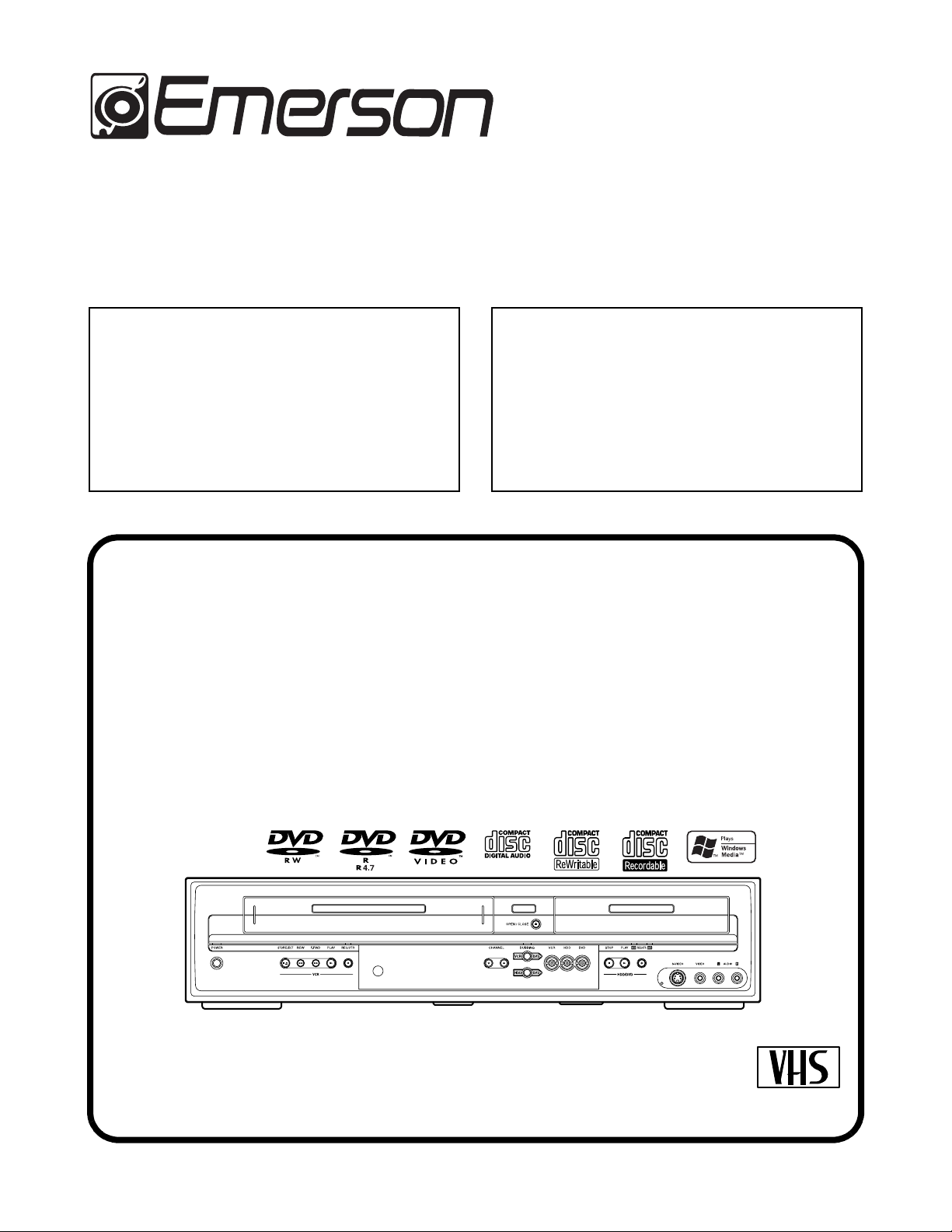
DVD/Video Cassette Recorder
The Part No. of the Deck
Mechanism used in this model is
N2461FL, but when servicing the
deck mechanism, refer to
N2460FL in the MK14 Deck
Mechanism Section.
with HDD
EWH100F
Page 2

IMPORTANT SAFETY NOTICE
Proper service and repair is important to the safe, reliable operation of all
Funai Equipment. The service procedures recommended by Funai and
described in this service manual are effective methods of performing
service operations. Some of these service special tools should be used
when and as recommended.
It is important to note that this service manual contains various CAUTIONS
and NOTICES which should be carefully read in order to minimize the risk
of personal injury to service personnel. The possibility exists that improper
service methods may damage the equipment. It also is important to
understand that these CAUTIONS and NOTICES ARE NOT EXHAUSTIVE.
Funai could not possibly know, evaluate and advice the service trade of all
conceivable ways in which service might be done or of the possible
hazardous consequences of each way. Consequently, Funai has not
undertaken any such broad evaluation. Accordingly, a servicer who uses a
service procedure or tool which is not recommended by Funai must first
use all precautions thoroughly so that neither his safety nor the safe
operation of the equipment will be jeopardized by the service method
selected.
Manufactured under license from Dolby Laboratories.
“Dolby” and the double-D symbol are trademarks of Dolby Laboratories.
Page 3

MAIN SECTION
DVD/Video Cassette Recorder
with HDD
EWH100F
Main Section
I Specifications
I Preparation for Servicing
I Adjustment Procedures
I Schematic Diagrams
I CBA’s
I Exploded Views
I Parts List
TABLE OF CONTENTS
Specifications . . . . . . . . . . . . . . . . . . . . . . . . . . . . . . . . . . . . . . . . . . . . . . . . . . . . . . . . . . . . . . . . . . . . . . . . . . 1-1-1
Laser Beam Safety Precautions . . . . . . . . . . . . . . . . . . . . . . . . . . . . . . . . . . . . . . . . . . . . . . . . . . . . . . . . . . . . 1-2-1
Important Safety Precautions . . . . . . . . . . . . . . . . . . . . . . . . . . . . . . . . . . . . . . . . . . . . . . . . . . . . . . . . . . . . . . 1-3-1
Standard Notes for Servicing . . . . . . . . . . . . . . . . . . . . . . . . . . . . . . . . . . . . . . . . . . . . . . . . . . . . . . . . . . . . . .1-4-1
Handling Precautions for HDD . . . . . . . . . . . . . . . . . . . . . . . . . . . . . . . . . . . . . . . . . . . . . . . . . . . . . . . . . . . . .1-5-1
Preparation for Servicing. . . . . . . . . . . . . . . . . . . . . . . . . . . . . . . . . . . . . . . . . . . . . . . . . . . . . . . . . . . . . . . . . .1-6-1
Cabinet Disassembly Instructions. . . . . . . . . . . . . . . . . . . . . . . . . . . . . . . . . . . . . . . . . . . . . . . . . . . . . . . . . . .1-7-1
Electrical Adjustment Instructions . . . . . . . . . . . . . . . . . . . . . . . . . . . . . . . . . . . . . . . . . . . . . . . . . . . . . . . . . . . 1-8-1
How to Self-Check and Initialize the DVD/VCR with HDD . . . . . . . . . . . . . . . . . . . . . . . . . . . . . . . . . . . . . . . . 1-9-1
Firmware Renewal Mode . . . . . . . . . . . . . . . . . . . . . . . . . . . . . . . . . . . . . . . . . . . . . . . . . . . . . . . . . . . . . . . . 1-10-1
Function Indicator Symbols. . . . . . . . . . . . . . . . . . . . . . . . . . . . . . . . . . . . . . . . . . . . . . . . . . . . . . . . . . . . . . . 1-11-1
Block Diagrams . . . . . . . . . . . . . . . . . . . . . . . . . . . . . . . . . . . . . . . . . . . . . . . . . . . . . . . . . . . . . . . . . . . . . . . .1-12-1
Schematic Diagrams / CBA’s and Test Points. . . . . . . . . . . . . . . . . . . . . . . . . . . . . . . . . . . . . . . . . . . . . . . . . 1-13-1
Waveforms . . . . . . . . . . . . . . . . . . . . . . . . . . . . . . . . . . . . . . . . . . . . . . . . . . . . . . . . . . . . . . . . . . . . . . . . . . . 1-14-1
Wiring Diagram . . . . . . . . . . . . . . . . . . . . . . . . . . . . . . . . . . . . . . . . . . . . . . . . . . . . . . . . . . . . . . . . . . . . . . . . 1-15-1
System Control Timing Charts . . . . . . . . . . . . . . . . . . . . . . . . . . . . . . . . . . . . . . . . . . . . . . . . . . . . . . . . . . . .1-16-1
IC Pin Function Descriptions. . . . . . . . . . . . . . . . . . . . . . . . . . . . . . . . . . . . . . . . . . . . . . . . . . . . . . . . . . . . . . 1-17-1
Lead Identifications . . . . . . . . . . . . . . . . . . . . . . . . . . . . . . . . . . . . . . . . . . . . . . . . . . . . . . . . . . . . . . . . . . . . . 1-18-1
Exploded Views. . . . . . . . . . . . . . . . . . . . . . . . . . . . . . . . . . . . . . . . . . . . . . . . . . . . . . . . . . . . . . . . . . . . . . . .1-19-1
Mechanical Parts List . . . . . . . . . . . . . . . . . . . . . . . . . . . . . . . . . . . . . . . . . . . . . . . . . . . . . . . . . . . . . . . . . . . 1-20-1
Electrical Parts List . . . . . . . . . . . . . . . . . . . . . . . . . . . . . . . . . . . . . . . . . . . . . . . . . . . . . . . . . . . . . . . . . . . . . 1-21-1
Page 4

SPECIFICATIONS
ITEM
General
HDD Internal 3.5 inch HDD 80 GB
Power consumption 44W (standby: 4.6W)
Recording
Recording format Video Recording Format (DVD-RW only)
Recordable discs DVD-ReWritable
Video recording format
Sampling frequency
Compression format
Audio recording format
Sampling frequency
Compression format
Tuner
Receivable channels
VHF
UHF
CATV
Input/Output
Video input
Input level
Jacks
S-Video input
Y (Iuminance) - Input level
C (color) - Input level
Jacks
Audio input
During audio input
Jacks
Component video output
Output level
Jacks
Video output
Output level
Jacks
S-Video output
Y (Iuminance) - Output level
C (color) - Output level
Jack
Audio output
During audio output
Jacks
Digital audio output
Output level
Jack
VHF/UHF antenna
input/output terminal VHF/UHF set 75Ω
Video Format (DVD-RW, DVD-R)
DVD-Recordable
13.5MHz
MPEG
48kHz
Dolby Digital
2-13ch
14-69ch
C1-C125ch
Input 1 (rear), 2 (front)
1 Vp-p (75Ω)
RCA jack
Input 1 (rear), 2 (front)
1 Vp-p (75Ω)
286 mVp-p (75Ω)
4 pin mini DIN
Input 1 (rear), 2 (front) L/R
2V rms (47kΩ)
RCA jacks
Y: 1.0 Vp-p (75Ω), P
RCA jacks
1 Vp-p (75Ω)
RCA jack
1 Vp-p (75Ω)
286 mVp-p (75Ω)
4 pin mini DIN
Output 1,2 L/R
2V rms (47kΩ)
RCA jacks
500 mVp-p (75Ω)
RCA jack
B/CB, PR/CR: 0.7 Vp-p (75Ω)
NOTES:
1. All Items are measured without pre-emphasis unless otherwise specified.
2. Power supply: AC120 V 60 Hz
3 Ambient temperature: 5
°C ~ 40 °C
1-1-1 E4340SP
Page 5
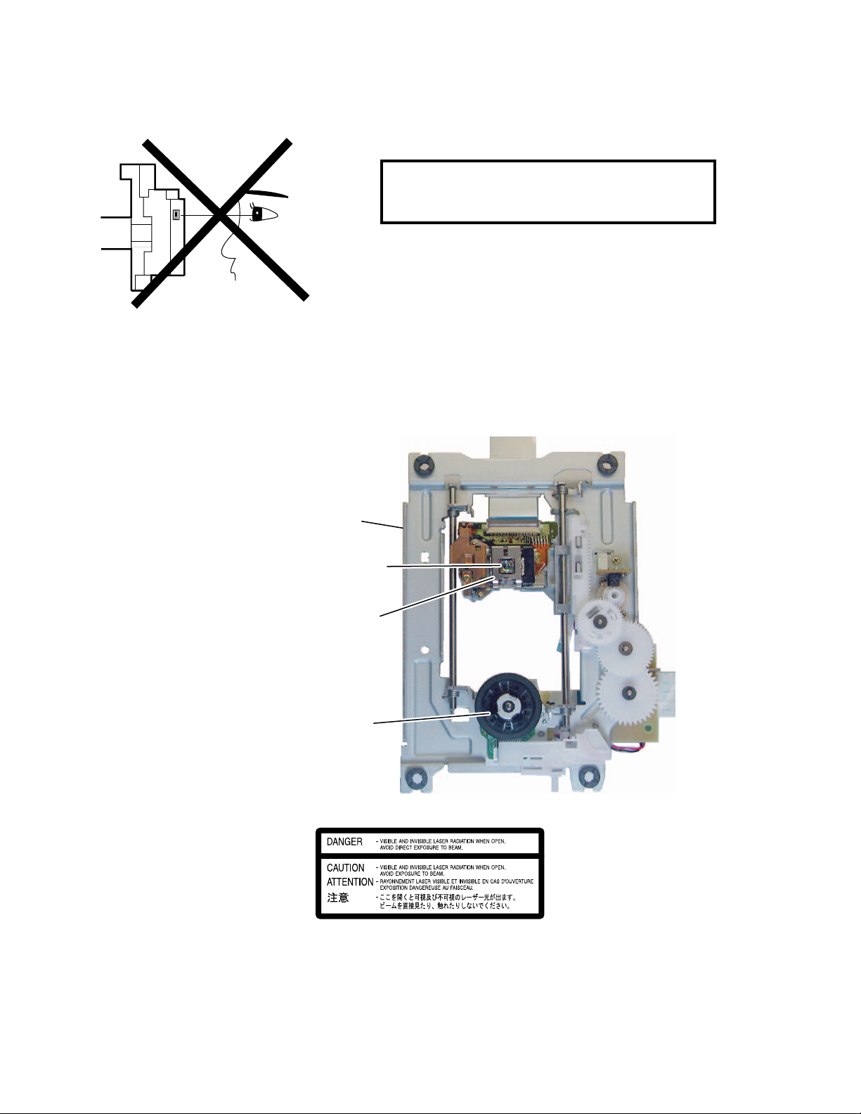
LASER BEAM SAFETY PRECAUTIONS
This DVD player uses a pickup that emits a laser beam.
Do not look directly at the laser beam coming
from the pickup or allow it to strike against your
skin.
The laser beam is emitted from the location shown in the figure. When checking the laser diode, be sure to keep
your eyes at least 30 cm away from the pickup lens when the diode is turned on. Do not look directly at the laser
beam.
CAUTION: Use of controls and adjustments, or doing procedures other than those specified herein, may result in
hazardous radiation exposure.
Drive Mechanism Assembly
Laser Beam Radiation
Laser Pickup
Turntable
Location: Inside Top of DVD mechanism.
1-2-1 R2NLSP
Page 6

IMPORTANT SAFETY PRECAUTIONS
Product Safety Notice
Some electrical and mechanical parts have special
safety-related characteristics which are often not
evident from visual inspection, nor can the protection
they give necessarily be obtained by replacing them
with components rated for higher voltage, wattage,
etc. Parts that have special safety characteristics are
identified by a # on schematics and in parts lists. Use
of a substitute replacement that does not have the
same safety characteristics as the recommended
replacement part might create shock, fire, and/or other
hazards. The Product’s Safety is under review
continuously and new instructions are issued
whenever appropriate. Prior to shipment from the
factory, our products are carefully inspected to confirm
with the recognized product safety and electrical
codes of the countries in which they are to be sold.
However, in order to maintain such compliance, it is
equally important to implement the following
precautions when a set is being serviced.
Precautions during Servicing
A. Parts identified by the # symbol are critical for
safety. Replace only with part number specified.
B. In addition to safety, other parts and assemblies
are specified for conformance with regulations
applying to spurious radiation. These must also be
replaced only with specified replacements.
Examples: RF converters, RF cables, noise
blocking capacitors, and noise blocking filters, etc.
C. Use specified internal wiring. Note especially:
1) Wires covered with PVC tubing
2) Double insulated wires
3) High voltage leads
D. Use specified insulating materials for hazardous
live parts. Note especially:
1) Insulation tape
2) PVC tubing
3) Spacers
4) Insulators for transistors
E. When replacing AC primary side components
(transformers, power cord, etc.), wrap ends of
wires securely about the terminals before
soldering.
F. Observe that the wires do not contact heat
producing parts (heat sinks, oxide metal film
resistors, fusible resistors, etc.).
G. Check that replaced wires do not contact sharp
edges or pointed parts.
H. When a power cord has been replaced, check that
5 - 6 kg of force in any direction will not loosen it.
I. Also check areas surrounding repaired locations.
J. Be careful that foreign objects (screws, solder
droplets, etc.) do not remain inside the set.
K. Crimp type wire connector
The power transformer uses crimp type
connectors which connect the power cord and the
primary side of the transformer. When replacing
the transformer, follow these steps carefully and
precisely to prevent shock hazards.
Replacement procedure
1) Remove the old connector by cutting the wires
at a point close to the connector.
Important: Do not re-use a connector.
(Discard it.)
2) Strip about 15 mm of the insulation from the
ends of the wires. If the wires are stranded,
twist the strands to avoid frayed conductors.
3) Align the lengths of the wires to be connected.
Insert the wires fully into the connector.
4) Use a crimping tool to crimp the metal sleeve at
its center. Be sure to crimp fully to the complete
closure of the tool.
L. When connecting or disconnecting the internal
connectors, first, disconnect the AC plug from the
AC outlet.
1-3-1 DVDN_ISP
Page 7
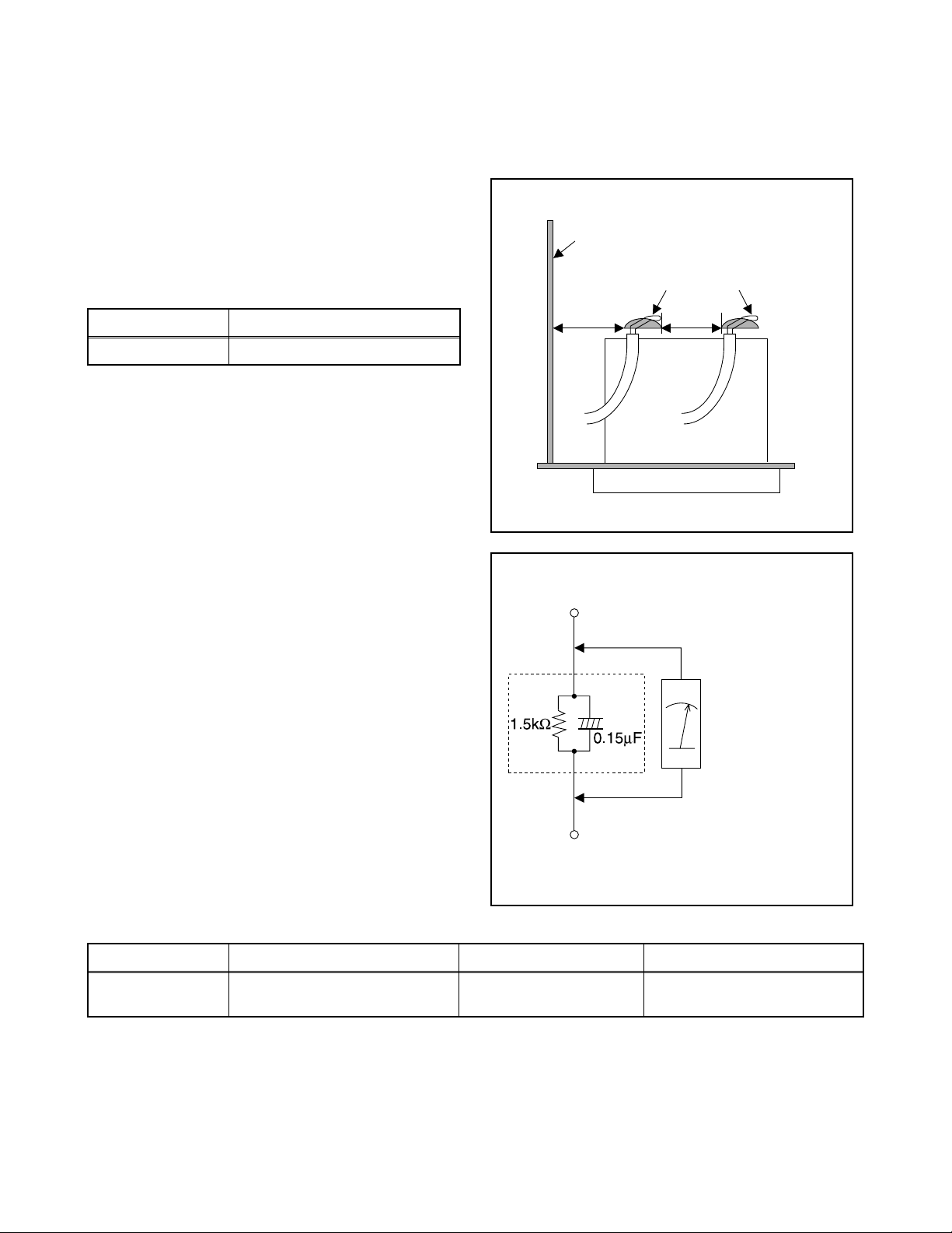
Safety Check after Servicing
Examine the area surrounding the repaired location for damage or deterioration. Observe that screws, parts, and
wires have been returned to their original positions. Afterwards, do the following tests and confirm the specified
values to verify compliance with safety standards.
1. Clearance Distance
When replacing primary circuit components, confirm
specified clearance distance (d) and (d’) between
soldered terminals, and between terminals and
surrounding metallic parts. (See Fig. 1)
Table 1: Ratings for selected area
Chassis or Secondary Conductor
Primary Circuit
AC Line Voltage Clearance Distance (d), (d’)
120 V ≥ 3.2 mm (0.126 inches)
Note: This table is unofficial and for reference only. Be
sure to confirm the precise values.
2. Leakage Current Test
Confirm the specified (or lower) leakage current
between B (earth ground, power cord plug prongs) and
externally exposed accessible parts (RF terminals,
antenna terminals, video and audio input and output
terminals, microphone jacks, earphone jacks, etc.) is
lower than or equal to the specified value in the table
below.
Measuring Method (Power ON):
Insert load Z between B (earth ground, power cord plug
prongs) and exposed accessible parts. Use an AC
voltmeter to measure across the terminals of load Z.
See Fig. 2 and the following table.
d' d
Fig. 1
Exposed Accessible Part
Z
AC Voltmeter
(High Impedance)
Earth Ground
B
Power Cord Plug Prongs
Table 2: Leakage current ratings for selected areas
AC Line Voltage Load Z Leakage Current (i) Earth Ground (B) to:
120 V
Note: This table is unofficial and for reference only. Be sure to confirm the precise values.
0.15 µF CAP. & 1.5 kΩ RES.
Connected in parallel
i ≤ 0.5 mA Peak Exposed accessible parts
1-3-2 DVDN_ISP
Fig. 2
Page 8
STANDARD NOTES FOR SERVICING
Circuit Board Indications
1. The output pin of the 3 pin Regulator ICs is
indicated as shown.
Top View
Out
2. For other ICs, pin 1 and every fifth pin are
indicated as shown.
Pin 1
3. The 1st pin of every male connector is indicated as
shown.
Pin 1
Input
In
Bottom View
5
10
Pb (Lead) Free Solder
When soldering, be sure to use the Pb free solder.
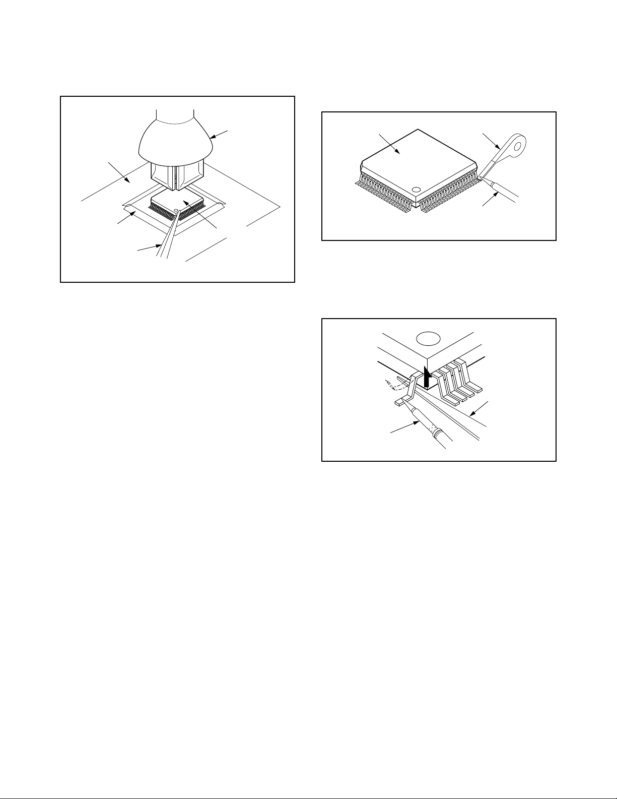
How to Remove / Install Flat Pack-IC
1. Removal
With Hot-Air Flat Pack-IC Desoldering Machine:
1. Prepare the hot-air flat pack-IC desoldering
machine, then apply hot air to the Flat Pack-IC
(about 5 to 6 seconds). (Fig. S-1-1)
Fig. S-1-1
Instructions for Connectors
1. When you connect or disconnect the FFC (Flexible
Foil Connector) cable, be sure to first disconnect
the AC cord.
2. FFC (Flexible Foil Connector) cable should be
inserted parallel into the connector, not at an
angle.
FFC Cable
Connector
CBA
* Be careful to avoid a short circuit.
2. Remove the flat pack-IC with tweezers while
applying the hot air.
3. Bottom of the flat pack-IC is fixed with glue to the
CBA; when removing entire flat pack-IC, first apply
soldering iron to center of the flat pack-IC and heat
up. Then remove (glue will be melted). (Fig. S-1-6)
4. Release the flat pack-IC from the CBA using
tweezers. (Fig. S-1-6)
CAUTION:
1. The Flat Pack-IC shape may differ by models. Use
an appropriate hot-air flat pack-IC desoldering
machine, whose shape matches that of the Flat
Pack-IC.
2. Do not supply hot air to the chip parts around the
flat pack-IC for over 6 seconds because damage
to the chip parts may occur. Put masking tape
around the flat pack-IC to protect other parts from
damage. (Fig. S-1-2)
1-4-1 DVDN_SN
Page 9
3. The flat pack-IC on the CBA is affixed with glue, so
be careful not to break or damage the foil of each
pin or the solder lands under the IC when
removing it.
With Soldering Iron:
1. Using desoldering braid, remove the solder from
all pins of the flat pack-IC. When you use solder
flux which is applied to all pins of the flat pack-IC,
you can remove it easily. (Fig. S-1-3)
CBA
Masking
Tape
Tweezers
Hot-air
Flat Pack-IC
Desoldering
Machine
Flat Pack-IC
Fig. S-1-2
Flat Pack-IC
Desoldering Braid
Soldering Iron
Fig. S-1-3
2. Lift each lead of the flat pack-IC upward one by
one, using a sharp pin or wire to which solder will
not adhere (iron wire). When heating the pins, use
a fine tip soldering iron or a hot air desoldering
machine. (Fig. S-1-4)
Sharp
Pin
Fine Tip
Soldering Iron
3. Bottom of the flat pack-IC is fixed with glue to the
CBA; when removing entire flat pack-IC, first apply
soldering iron to center of the flat pack-IC and heat
up. Then remove (glue will be melted). (Fig. S-1-6)
4. Release the flat pack-IC from the CBA using
tweezers. (Fig. S-1-6)
Fig. S-1-4
1-4-2 DVDN_SN
Page 10
With Iron Wire:
1. Using desoldering braid, remove the solder from
all pins of the flat pack-IC. When you use solder
flux which is applied to all pins of the flat pack-IC,
you can remove it easily. (Fig. S-1-3)
2. Affix the wire to a workbench or solid mounting
point, as shown in Fig. S-1-5.
3. While heating the pins using a fine tip soldering
iron or hot air blower, pull up the wire as the solder
melts so as to lift the IC leads from the CBA
contact pads as shown in Fig. S-1-5.
4. Bottom of the flat pack-IC is fixed with glue to the
CBA; when removing entire flat pack-IC, first apply
soldering iron to center of the flat pack-IC and heat
up. Then remove (glue will be melted). (Fig. S-1-6)
5. Release the flat pack-IC from the CBA using
tweezers. (Fig. S-1-6)
Note: When using a soldering iron, care must be
taken to ensure that the flat pack-IC is not
being held by glue. When the flat pack-IC is
removed from the CBA, handle it gently
because it may be damaged if force is applied.
Hot Air Blower
2. Installation
1. Using desoldering braid, remove the solder from
the foil of each pin of the flat pack-IC on the CBA
so you can install a replacement flat pack-IC more
easily.
2. The “● ” mark on the flat pack-IC indicates pin 1.
(See Fig. S-1-7.) Be sure this mark matches the 1
on the PCB when positioning for installation. Then
presolder the four corners of the flat pack-IC. (See
Fig. S-1-8.)
3. Solder all pins of the flat pack-IC. Be sure that
none of the pins have solder bridges.
Example :
Pin 1 of the Flat Pack-IC
is indicated by a " " mark.
Fig. S-1-7
To Solid
Mounting Point
CBA
Tweezers
Iron Wire
Soldering Iron
Fig. S-1-5
Fine Tip
Soldering Iron
Flat Pack-IC
or
Presolder
Flat Pack-IC
CBA
Fig. S-1-8
Fig. S-1-6
1-4-3 DVDN_SN
Page 11
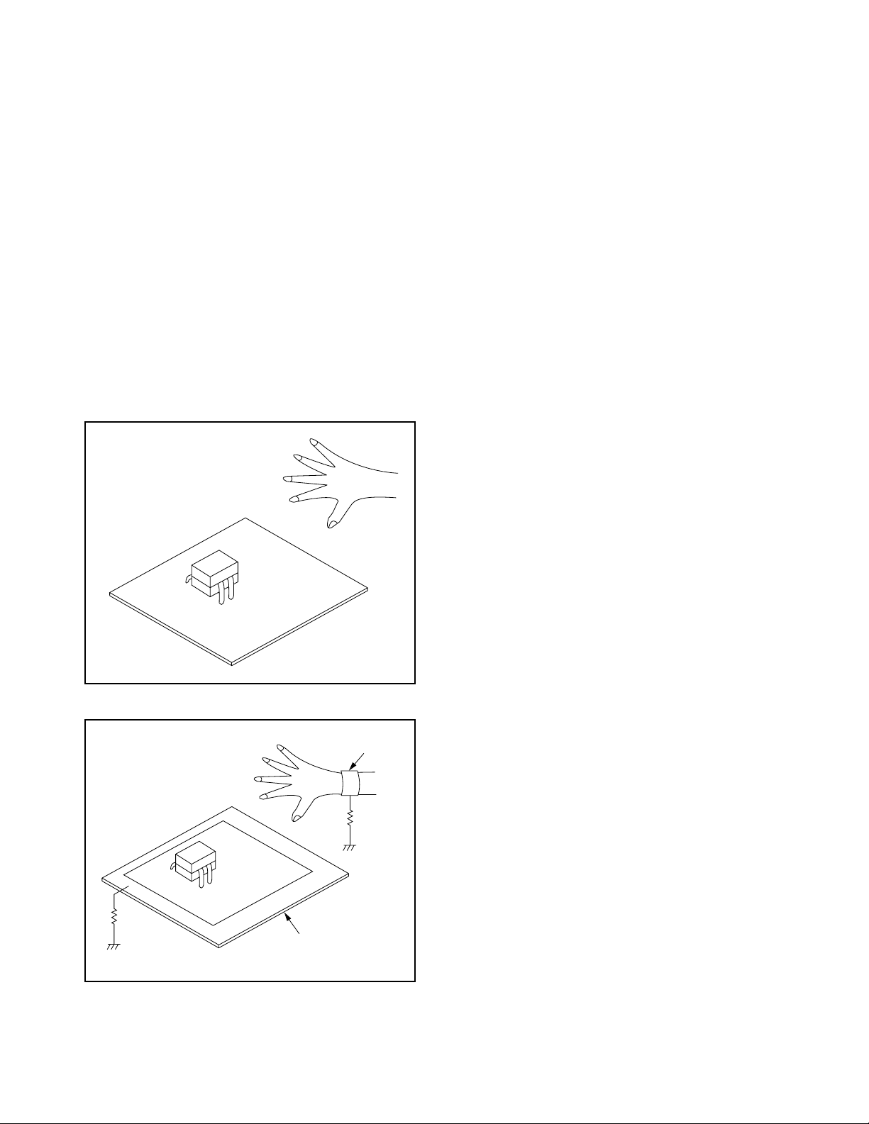
Instructions for Handling Semiconductors
Electrostatic breakdown of the semi-conductors may
occur due to a potential difference caused by
electrostatic charge during unpacking or repair work.
1. Ground for Human Body
Be sure to wear a grounding band (1 MΩ) that is
properly grounded to remove any static electricity that
may be charged on the body.
2. Ground for Workbench
Be sure to place a conductive sheet or copper plate
with proper grounding (1 MΩ) on the workbench or
other surface, where the semi-conductors are to be
placed. Because the static electricity charge on
clothing will not escape through the body grounding
band, be careful to avoid contacting semi-conductors
with your clothing.
<Incorrect>
<Correct>
1MΩ
CBA
Grounding Band
1MΩ
CBA
Conductive Sheet or
Copper Plate
1-4-4 DVDN_SN
Page 12

HANDLING PRECAUTIONS FOR HDD
CAUTION:
1. SHOCK
a. Exposing HDD to shock may be the biggest
damaging factor. Please note that HDD is easily
damaged even if dropped from any height. Be sure
to place HDD on a shock-absorbent mat. Also, be
careful when transporting HDD.
b. Be careful not to subject HDD to any shock when
tightening screws for HDD replacement.
(Tighten screws manually, not with an electric
driver.)
2. MOISTURE
a. Moisture may also be a damaging factor. HDD is
semiclosed style. Sudden changes in ambient
temperature may cause moisture to form. Monitor
temperature and do not allow moisture to form on
the media surface. Also, when opening HDD
package, do so only after package is at ambient
temperature.
b. After replacing HDD, leave it to reach room
temperature (about 2 hours) for preventing dew
internal condensation, and then work necessary
task such as operation check.
4. OTHERS
a. Be careful so as not to do the followings.
Otherwise, HDD might be damaged.
- DO NOT disassemble HDD.
- When handling HDD, be sure to hold both sides
securely.
b. HDD should be stored, packed in the protective
bag, in suitable surroundings (i.e., no extreme
changes in temperature to avoid condensation).
c. When transporting HDD, be sure to use the
exclusive packing case (the replacement HDD
carton).
d. Do not stack HDDs.
e. Do not place vertically because HDD is unstable
and easy to fall.
3. STATIC ELECTRICITY
a. After removing HDD or taking replacement HDD
out of the protective bag (the replacement HDD is
packed in a protective bag), place HDD on a
conductive surface. A grounding band should be
worn when handling.
Grounding Band
Both the conductive surface and grounding band
should be grounded.
b. Make sure that HDD is placed on main unit
completely and then let go of it, when assembling.
c. Do not put HDD on a packing bag. (for preventing
electrostatic damage)
1-5-1 DHDN_SN
Page 13
PREPARATION FOR SERVICING
How to Enter the Service Mode
About Optical Sensors
Caution:
An optical sensor system is used for the Tape Start
and End Sensors on this equipment. Carefully read
and follow the instructions below. Otherwise the unit
may operate erratically.
What to do for preparation
Insert a tape into the Deck Mechanism Assembly and
press [VCR PLAY] button. The tape will be loaded into
the Deck Mechanism Assembly. Make sure the power
is on, connect TP4502 (S-INH) to GND. This will stop
the function of Tape Start Sensor, Tape End Sensor
and Reel Sensors. (If these TPs are connected before
plugging in the unit, the function of the sensors will
stay valid.) See Fig. 1.
Q503
Note: Because the Tape End Sensors are inactive, do
not run a tape all the way to the start or the end of the
tape to avoid tape damage.
Q504
TP4502
S-INH
Fig. 1
1-6-1 E4340PFS
Page 14
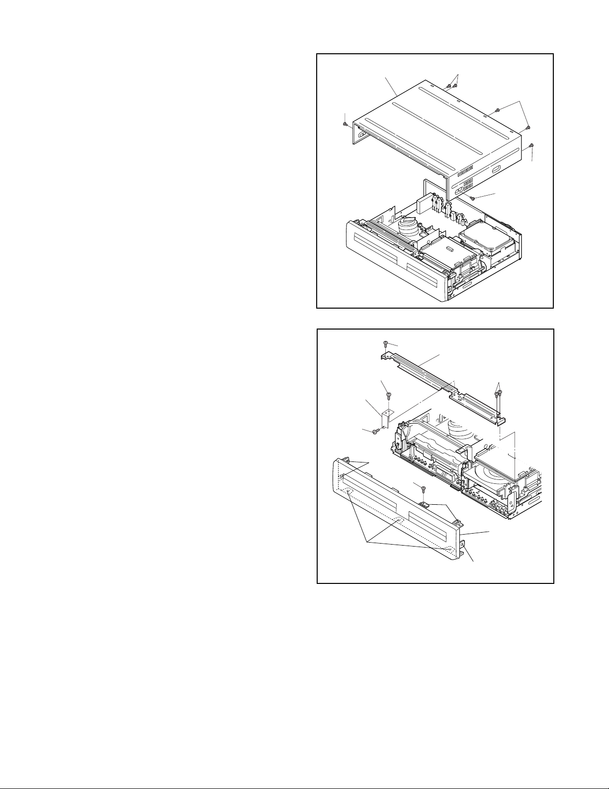
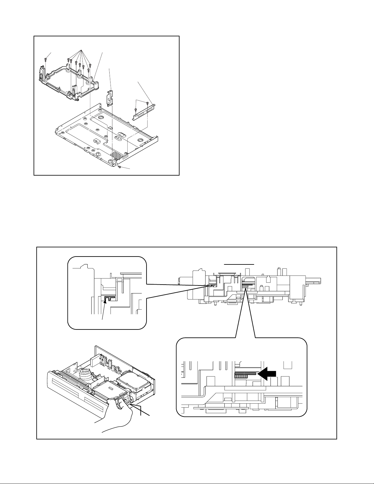
CABINET DISASSEMBLY INSTRUCTIONS
1. Disassembly Flowchart
This flowchart indicates the disassembly steps to gain
access to item(s) to be serviced. When reassembling,
follow the steps in reverse order. Bend, route, and
dress the cables as they were originally.
[1] Top Cover
[2] Front
Assembly
[21] Front
Bracket R
[22] Bracket R
[13] Power
Supply CBA
[14] Open/
Close CBA
[15] Front
Jack CBA
[3] Front
Bracket
[4] HDD
Assembly
[5] DVD
Mechanism &
DVD/HDD Main
CBA Assembly
[10] Fan
Holder
[11] Fan Motor
[12] Rear
Panel
[16] VCR
Chassis Unit
[17] Deck
Assembly
[18] AV CBA
[6] HDD
Bracket
[7] HDD Unit
[8] HDD
Support
[9] ATA CBA
[19] Power
SW CBA
ID/
LOC.
No.
PA RT
REMOVE/*UNHOOK/
Fig.
UNLOCK/RELEASE/
No.
UNPLUG/DESOLDER
Note
DVD
REMOVAL
[5]
Mechanism
& DVD/
HDD Main
CBA
2(S-5), 2(S-6),
D3
*CN2201, *CN4001,
Wiresheet
Assembly
HDD
[6]
Bracket
D4 4(S-7) ---
[7] HDD Unit D4 4(S-8), HDD Rubber 3
HDD
[8]
Support
D4 ---------- ---
[9] ATA CBA D4 *CN3001, *CN3002 --[10] Fan Holder D5 2(S-9) --[11] Fan Motor D5 *CN2204 --[12] Rear Panel D5 5(S-10), 2(S-11) ---
Power
[13]
Supply
D6 *CN2202, 2(S-12) ---
CBA
Open/
[14]
[15]
[16]
Close CBA
Front Jack
CBA
VCR
Chassis
Unit
D6 (S-13), Desolder ---
D6 *CN2501, 2(S-14) ---
5(S-15), 4(S-16),
D7
(S-17)
2
---
[20] Deck
Pedestal
2. Disassembly Method
ID/
LOC.
No.
PART
Fig.
No.
[1] Top Cover D1 7(S-1) ---
Front
[2]
[3]
[4]
Assembly
Front
Bracket
HDD
Assembly
D2 (S-2), *5(L-1), *3(L-2)11-1
D2
D3
REMOVAL
REMOVE/*UNHOOK/
UNLOCK/RELEASE/
UNPLUG/DESOLDER
2(S-3), 3(S-3B), Front
Support
3(S-4), *CN201,
*CN2203
[17]
Deck
Assembly
(S-18), (S-19)
D8
Desolder
[18] AV CBA D8 ---------- ---
Power SW
Note
[19]
[20]
[21]
CBA
Deck
Pedestal
Front
Bracket R
D8 Desolder ---
D9 8(S-20) ---
D9 (S-21) ---
[22] Bracket R D9 2(S-22) ---
1-2
↓
(1)
↓
(2)
↓
(3)
↓
(4)
---
Note:
---
(1): Identification (location) No. of parts in the figures
(2): Name of the part
(3): Figure Number for reference
1-7-1 E4340DC
4
5
↓
(5)
Page 15
(4): Identification of parts to be removed, unhooked,
unlocked, released, unplugged, unclamped, or
desoldered.
P=Spring, L=Locking Tab, S=Screw,
CN=Connector
*=Unhook, Unlock, Release, Unplug, or Desolder
e.g. 6(S-1) = six Screws (S-1),
5(L-1) = five Locking Tabs (L-1)
(5): Refer to “Reference Notes.”
[1] Top Cover
(S-1)
(S-1)
(S-1)
Reference Notes
1. Locking Tabs (L-1) and (L-2) are fragile. Be careful
not to break them.
1-1. Remove Screw (S-2).
1-2. Release five Locking Tabs (L-1).
1-3. Release three Locking Tabs (L-2) and
remove the Front Assembly.
2. Do not replace the DVD Mechanism or the DVD/
HDD Main CBA Assembly separately, when
replacing the DVD Mechanism & DVD/HDD Main
CBA Assembly. Order the new DVD Mechanism &
DVD/HDD Main CBA Assembly.
3-1. Whenever you have replaced the HDD unit,
initialize the HDD unit. To initialize the HDD
unit, perform the following.To put the DVD/
VCR with HDD recorder into the HDD mode,
press the [HDD] button on the remote control
unit.
3-2. To put the DVD/VCR with HDD recorder into
the self-check mode, after pressing
[VARIABLE SKIP] button, press the [3], [6],
and [9] buttons on the remote control in that
order within three seconds.
3-3. Press [ENTER] button. The DVD/VCR with
HDD recorder is initialized and the power is
turned off automatically after two seconds.
3. When reassembling, solder wire jumpers as
shown in Fig. D8.
4. Before installing the Deck Assembly, be sure to
place the pin of LD-SW on the AV CBA as shown
in Fig. D8. Then, install the Deck Assembly while
aligning the hole of Cam Gear with the pin of LDSW, the shaft of Cam Gear with the hole of LD-SW
as shown in Fig. D8.
Front
Support
(S-3B)
(L-2)
(S-3B)
(L-1)
(S-1)
(S-1)
Fig. D1
(S-3B)
[3] Front Bracket
(S-3)
(S-2)
(L-1)
[2] Front
Assembly
(L-1)
Fig. D2
1-7-2 E4340DC
Page 16
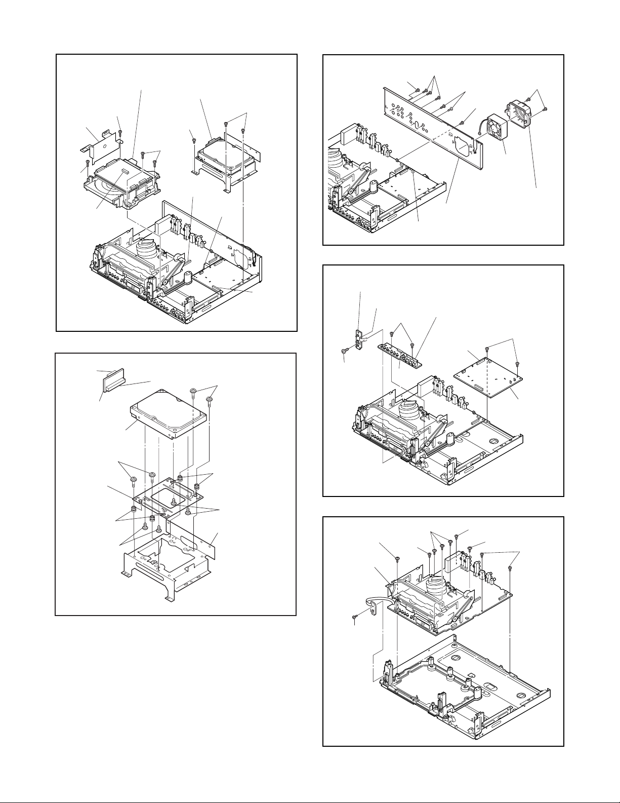
[5] DVD Mechanism &
DVD/HDD Main CBA
Assembly
Wire
Sheet
(S-6)
[4] HDD Assembly
(S-4)
(S-4)
(S-11)
(S-10)
(S-10)
(S-11)
(S-9)
(S-6)
CN201
CN3002
[9] ATA CBA
[7] HDD Unit
(S-5)
CN4001
CN3001
CN2203
(S-7)
CN2201
Fig. D3
[14] Open/Close CBA
Desolder
(S-14)
(S-13)
CN2501
[11] Fan
Motor
[10] Fan Holder
[12] Rear Panel
CN2204
Fig. D5
[15] Front Jack CBA
(S-12)
CN2202
[13] Power
Supply CBA
(S-7)
[8] HDD
Support
HDD Rubber
(S-8)
HDD Rubber
(S-8)
[6] HDD Bracket
Fig. D4
(S-15)
[16] VCR
Chassis
Unit
(S-17)
(S-15)
(S-16)
Fig. D6
(S-16)
(S-15)
(S-16)
Fig. D7
1-7-3 E4340DC
Page 17
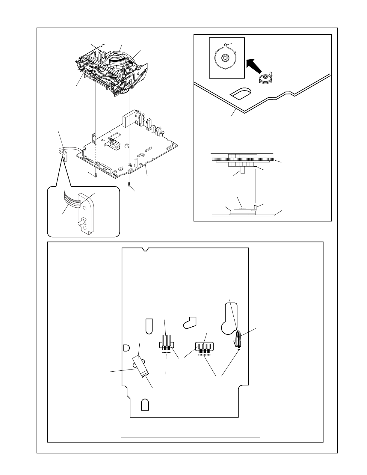
FE Head
[17] Deck
Assembly
Cylinder
Assembly
ACE Head
Assembly
Pin
Pin
SW4512
LD-SW
[19] Power
SW CBA
(S-18)
Lead with
blue stripe
Desolder
[18] AV CBA
(S-19)
Printing side
From
ACE Head
Assembly
[18] AV CBA
[17] Deck Assembly
Shaft
Hole
LD-SW
From
FE Head
From
Cylinder
Assembly
Cam Gear
Hole
Pin
[18] AV CBA
Lead with
gray stripe
From
Capstan
Motor
Assembly
Lead with
blue stripe
Desolder
Desolder
Desolder
BOTTOM VIEW
Lead connections of Deck Assembly and AV CBA
1-7-4 E4340DC
Fig. D8
Page 18
(S-20)
(S-20)
[20] Deck Pedestal
[21] Front Bracket R
[22] Bracket R
(S-22)
(S-21)
Fig. D9
3. How to Eject Manually
< Method 1 >
Note: When servicing, do not touch white resin part as shown below.
When rotating the gear, be careful not to damage the gear.
1. Remove the Top Cover.
2. Rotate the gear in the direction of the arrow manually as shown below.
View for A
Do not touch!
Rotate this gear in
the direction of the arrow
A
1-7-5 E4340DC
Page 19
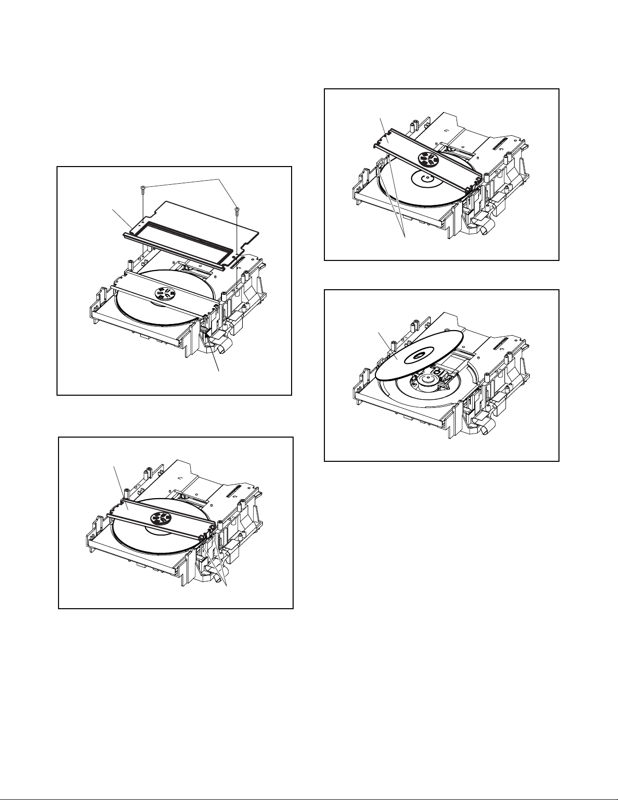
< Method 2 >
Note: When servicing, do not touch white resin part
as shown below.
1. Remove the Top Cover, the Front Assembly and
the DVD Mechanism & DVD/HDD Main CBA
Assembly. Then, remove the DVD Mechanism
Unit.
2. Remove two screws, and remove the Insulating
Plate.
Screw
Insulating Plate
4. Release the other side of two Locking Tabs, and
remove the Clamper Assembly.
Clamper Assembly
Locking Tabs
5. Remove the disc.
Disc
Do not touch!
3. Release two Locking Tabs, and lift up one side of
the Clamper Assembly.
Clamper Assembly
Locking Tabs
6. Assemble the DVD Mechanism and DVD/HDD
Main CBA.
Note: The combination of the DVD Mechanism
and the DVD/HDD Main CBA cannot be changed.
When assembling the DVD/HDD Main CBA on the
DVD Mechanism, use the DVD/HDD Main CBA
that disassembled on the item 1. The other DVD/
HDD Main CBA cannot be used.
1-7-6 E4340DC
Page 20
ELECTRICAL ADJUSTMENT INSTRUCTIONS
General Note: “CBA” is abbreviation for
“Circuit Board Assembly.”
NOTE:
1. Electrical adjustments are required after replacing
circuit components and certain mechanical parts.
It is important to do these adjustments only after
all repairs and replacements have been
completed. Also, do not attempt these adjustments
unless the proper equipment is available.
2. To perform these alignment / confirmation
procedures, make sure that the tracking control is
set in the center position: Press either [CHANNEL
L] or [CHANNEL K] button on the front panel first,
then the [VCR PLAY] button on the front panel.
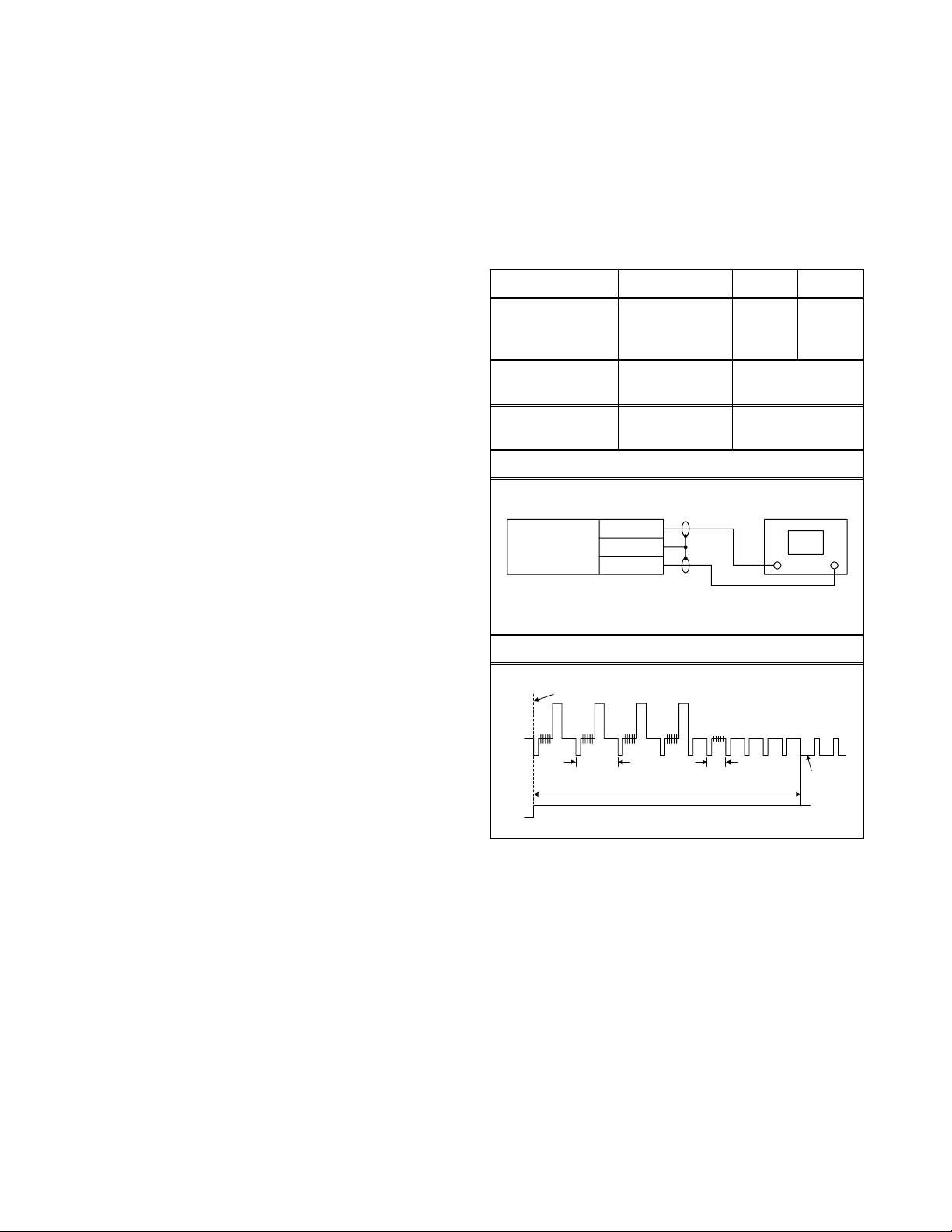
Test Equipment Required
1. Oscilloscope: Dual-trace with 10:1 probe,
V-Range: 0.001~50 V/Div.,
F-Range: DC~AC-20 MHz
2. Alignment Tape (FL8A)
Head Switching Position
Adjustment
Purpose: To determine the Head Switching position
during playback.
Symptom of Misadjustment: May cause Head
Switching noise or vertical jitter in the picture.
Test point Adj. Point Mode Input
JP4017(V-OUT)
TP4302(RF-SW)
GND
Tape
FL8A Oscilloscope
Connections of Measurement Equipment
AV CBA
VR4501
(Switching
Point)
Measurement
Equipment
JP4017
GND
TP4302
PLAY
(SP)
6.5H ± 1H
(412.7µs±63.5µs)
Oscilloscope
-----
Spec.
CH1 CH2
Trig. (+)
Figure 1
EXT. Syncronize Trigger Point
CH1
CH2
Note: JP4017 (V-OUT), TP4302 (RF-SW),
Reference Notes:
Playback the Alignment tape and adjust VR4501 so
that the V-sync front edge of the CH1 video output
waveform is at the 6.5H ± 1H (412.7 µs ± 63.5 µs)
delayed position from the rising edge of the CH2 head
switching pulse waveform.
1.0H
6.5H±1H (412.7µs±63.5µs)
Switching Pulse
VR4501 (Switching Point) --- AV CBA
0.5H
V-Sync
1-8-1 E4340EA
Page 21
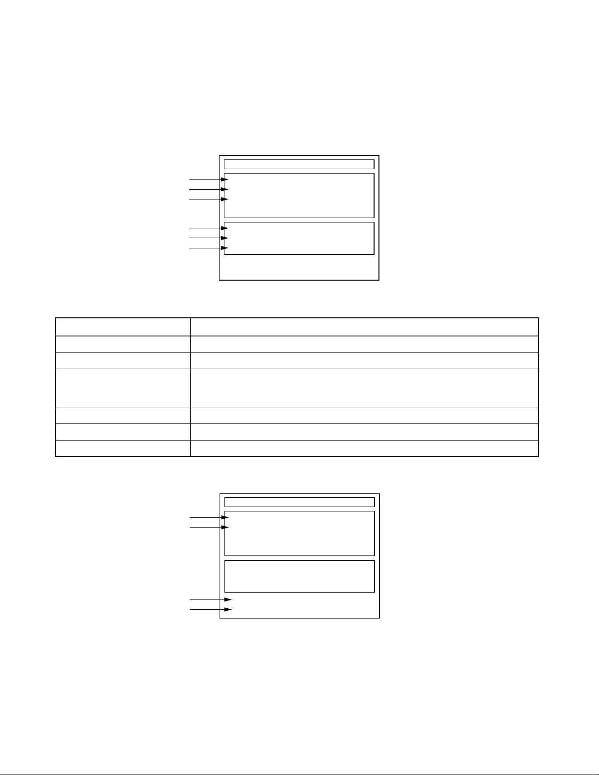
HOW TO SELF-CHECK AND INITIALIZE THE DVD/VCR WITH HDD
1. Turn on the DVD/VCR with HDD recorder.
2. To put the DVD/VCR with HDD recorder into the HDD mode, press [HDD] on the remote control unit.
3. To put the DVD/VCR with HDD recorder into the self-check mode, after pressing [VARIABLE SKIP] button,
press the [3], [6], and [9] buttons on the remote control in that order within three seconds.
Fig. a appears on the screen and all LEDs light.
"
" differs depending on the models.
*******
Self-Analysys and Report
*1
*2
*3
DVD CONNECT STATUS :
HDD CONNECT STATUS :
HDD POWER ON HOURS :
*4
*5
*6
BE Ver. :
FE Ver. :
Sub Micon Ver. :
T2*******Q2J
R20_0**_***h
NFQ2***T1-3N11
Fig. a: Self-Check Mode Screen
Table 1: Description of Fig. a
INDICATION DESCRIPTION
DVD CONNECT STATUS (*1) Connecting Condition of DVD(F/E)
HDD CONNECT STATUS (*2) Connecting Condition of HDD
Value of HDD power on hours obtained from S.M.A.R.T. command. (If not obtainable,
HDD POWER ON HOURS (*3)
value of HDD power on hours is “0”.)
Value in parentheses is the factory setting value. (If no setting, the value is “0”.)
BE Ver. (*4) B/E version
FE Ver. (*5) F/E version
Sub Micon Ver. (*6) Sub micro controller version
4. Upon the self-check completion, Fig. b appears on the screen.
"
" differs depending on the models.
*******
Self-Analysys and Report
*7
*8
DVD CONNECT STATUS : OK
HDD CONNECT STATUS : OK
HDD POWER ON HOURS : 100(40)
*10
BE Ver. :
FE Ver. :
Sub Micon Ver. :
*9
FACTORY DEFAULT :
POWER OFF :
T2*******Q2J
R20_0**_***h
NFQ2***T1-3N11
ENTER
POWER
Fig. b: Screen of Finishing Self-Check Mode
1-9-1 E4340INT
Page 22
Table 2: Indication of DVD self-check (*7)
INDICATION DESCRIPTION
OK Connection of DVD is normal.
NOT FOUND DVD drive cannot be found.
CABLE ERROR
FFC cable (connecting to CN401) between the DVD drive and the DVD/HDD Main CBA is
not connected correctly.
Table 3: Indication of HDD self-check (*8)
INDICATION DESCRIPTION
OK Connection of HDD is normal.
NOT FOUND HDD drive cannot be found.
CABLE ERROR FFC cable between the ATA CBA and the HDD drive is not connected correctly.
Table 4: Available button in self-check mode
BUTTON DESCRIPTION
ENTER (*9) Initialize (only when the self-check mode is complete)
POWER (*10) Turn the power off (when the self-check mode is complete)
OTHER Not available
5. When the self-check mode is complete, press [POWER] button to turn the power off.
When initializing the DVD/VCR with HDD recorder, press [ENTER] button. Fig. c appears on the screen. After
two seconds, the power is turned off automatically.
"
" differs depending on the models.
*******
Self-Analysys and Report
DVD CONNECT STATUS : OK
HDD CONNECT STATUS : OK
HDD POWER ON HOURS : 100(40)
BE Ver. :
FE Ver. :
Sub Micon Ver. :
FACTORY DEFAULT : *11WRITING
T2*******Q2J
R20_0**_***h
NFQ2***T1-3N11
Fig. c: Initialize Mode Screen
Table 5: Description of *11 in Fig. c
INDICATION DESCRIPTION
ENTER Initialization preparation is complete.
WRITING Initializing
OK Initializing is finished normally.
NG Initializing is not finished normally.
NOTE: When initializing, “Current Clock”, “Setup Changing Item”, “Channel Setup”, “Area Setup”, “Program” and
“HDD Contents” are initialized.
1-9-2 E4340INT
Page 23
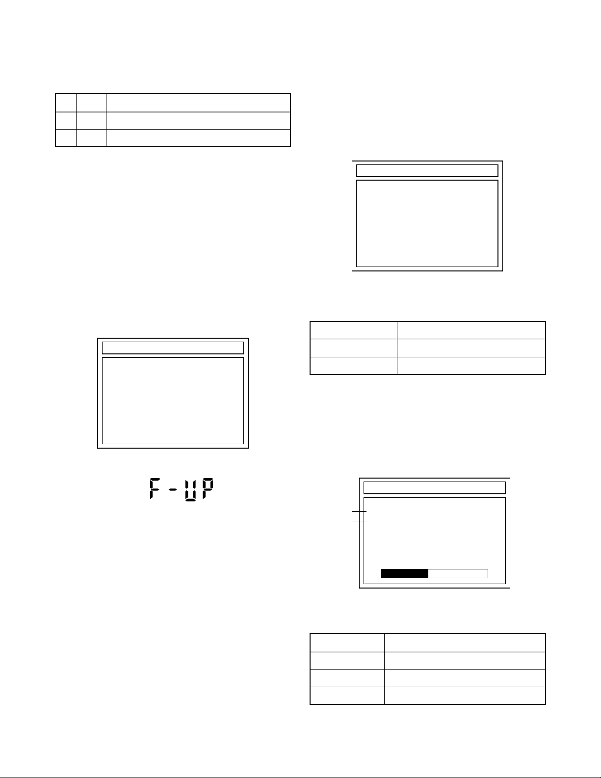
FIRMWARE RENEWAL MODE
1. Update Contents
Item Status
1 B/E Update B/E FIRMWARE
2 F/E Update F/E FIRMWARE
2. Update
1. Turn the power on and remove the disc in the tray.
2. To switch the DVD/VCR with HDD recorder into
the HDD mode, press [HDD] on the remote control
unit.
3. To put the DVD/VCR with HDD recorder into
version up mode, press [VARIABLE SKIP] and [6],
[5], [4] buttons on the remote control unit in that
order within 3 seconds. The tray will open
automatically.
Fig. a appears on the TV screen and Fig. b
appears on the VFD.
*FIRMWARE version will differ depending on the
model. Fig. a is an example.
DISC UPDATE
4. Load the update disc.
The TV screen will display Fig. c.
- If the update disc contains only a single file, the
update will initiate automatically when the disc is
inserted.
*FIRMWARE version will differ depending on the
model. Fig. c is an example.
DISC UPDATE
<DIR> BE
<DIR> FE
Fig. c: Update Disc TV Screen
Effective FIRMWARE update files will have the file
extensions shown below.
File extension Status
BIN B/E FIRMWARE file
Please Insert F/W Disc
Fig. a: Update Mode TV Screen
Fig. b: VFD Display in Update Mode
MOT F/E FIRMWARE file
5. Select the desired FIRMWARE to be updated with
the arrow button and press the [ENTER] button.
FIRMWARE will automatically select the
appropriate F/E or B/E version.
Fig. d appears on the TV screen and Fig. e
appears on the VFD, and the update will start.
*FIRMWARE version will differ depending on the
model. Fig. d is an example.
DISC UPDATE
*1
TARGET: B/E
*2
STATUS: EXECUTING
DISC UPDATING xx% Complete
Fig. d: TV Display during update
The status displayed in *1 is as shown below.
Display Status
B/E FIRMWARE B/E
F/E FIRMWARE F/E
UNKNOWN Not FIRMWARE B/E or F/E
1-10-1 E4340FW
Page 24
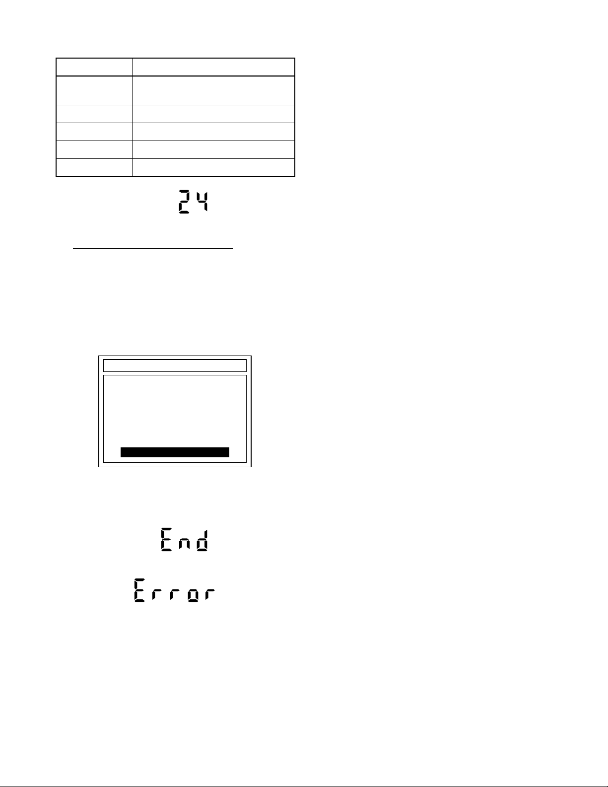
The status displayed in *2 is as shown below.
3. How to Verify the Firmware
Display Status
EXECUTING
Loading F/W from Update Disc or
writing to Flash memory
OK Update successful
ERROR Error during Flash memory writing
FILE ERROR Check SAM error in F/W file
READ ERROR Error during F/W file reading
Fig. e: VFD Display during update
Re: the VFD display shown in Fig. e.
When the TV screen displays "Firmware
Updating... XX% Complete," the VFD will indicate
"XX"%.
6. When completing update, the tray will open
automatically.
The TV screen will display Fig. f.
*FIRMWARE version will differ depending on the
model. Fig. f is an example.
Version
1. Turn the power on and remove the disc in the tray.
2. To switch the DVD/VCR with HDD recorder into
the HDD mode, press [HDD] on the remote control
unit.
3. Press [VARIABLE SKIP] and [1], [2], [3] buttons on
the remote control unit in that order within 3
seconds. The Firmware version appears on the TV
screen.
4. Press [POWER] button to reset the unit.
DISC UPDATE
TARGET: B/E
STATUS: OK
DISC UPDATING 100% Complete
PLEASE PUSH POWER BUTTON
Fig. f: TV Display when completing update
If the update is completed correctly, the VFD will
indicate Fig. g.
Fig. g: VFD Display when completing update
Fig. h VFD Display when completing update with error
In this case, all button operations will be invalid
except [POWER] button.
7. Press [POWER] button to turn the power off and
press [POWER] button again to turn the power on
and finish updating.
1-10-2 E4340FW
Page 25

FUNCTION INDICATOR SYMBOLS
< VCR Section >
Note:
If a mechanical malfunction occurs, the power is turned off. The following symbols will appear on the display.
Status Display
When reel or capstan mechanism is not
functioning correctly
When tape loading mechanism is not
functioning correctly
When cassette loading mechanism is not
functioning correctly
When the drum is not working properly
P-ON+5V Power safety detection
“W” blinks.
Fan does not rotate over 30 seconds.
When the power comes on again after that by pressing [POWER] button, an error message is displayed on the TV
screen as follows.
When reel or capstan mechanism is not functioning
correctly
A
R
SP 0:00:00
When tape loading mechanism is not functioning
correctly
A
T
SP 0:00:00
“W” light and “R” blinks.
When the drum is not working properly
A
D
SP 0:00:00
Fig. 1
P-ON+5V Power safety detection
A
P
SP 0:00:00
Fig. 4
Fig. 2
When cassette loading mechanism is not functioning
correctly
A
C
SP 0:00:00
Fig. 3
Fig. 5
1-11-1 E4340FIS
Page 26
< DVD/HDD Section >
Note: If an error occurs, a message with the error number appears on the screen.
Recording Error
02-50
Error message
Error No.
Message Error No. Error Description Error Example
Disc error
Recording
error
System error
04-50
04-51
03-50
03-52 Loader error
03-53 Poor media
03-54
03-55 Writing error (video)
03-56 General error
03-57 Device error
03-60 Unrecordable disc
02-50
02-51 Disc protection failure
02-52 Format failure
02-53 Abnormal loader This code is output when an appropriate DVD drive is not connected.
02-54
02-55
02-56
02-57 Fan lock
02-58 F/E hang-up
02-59 HDD hang-up
Renewal error at
ejecting disc
Disc includes still
picture
Recording error
caused by media
error
Control information
error and control data
error
Erasing error (all
titles)
Abnormal HDD
mount
Changing status
failure during VCR
dubbing
Abnormal VCR
mechanism
This code is output when there is a control information writing failure
due to tray being open during writing or disc loading.
This code is output upon attempt to write data (finalizing disc protect
data, etc.) on a disc including a still picture.
This code is output when recording error caused by media error
occurs, e.g.,stopping recording during attempting to record on a
scratched disc.
This code is output when tray open/close error occurs. Also, when
the tray open error occurs at F/E and when the recovery fails even if
the B/E retries.
This code is output when a DVD operation error occurs during
copying.
This code is output when a chip (EMMA) outputs unusual data while
recording and the control information writing fails.
This code is output when video writing fails while copying at high
speed.
This code is output when a number of errors occur:
Ex.1) When Outplay list creation fails.
Ex.2) When the system can’t take the title information which should
be written on the disc.
Ex3) When starting to copy, recording is paused and restarted but,
after the recording pause, recording start fails.
This code is output when an HDD operation error occurs (HDD
recording error), while copying at high speed or constant speed.
This code is output when recording is attempted on a non recordable disc such as a CD or DVD-ROM.
This code is output when an error occurs erasing entire VR playlist,
HDD playlist or HDD originals.
This code is output when protected pre-existing information that
should be on a disc is missing (VR disc protection error).
This code is output when HDD formatting occurs in maintenance
mode.
This code is output when a [PLAY], [STOP], [REC], [MENU] or [LIST]
button is pressed while HDD is not functional.
This code is output when, during dubbing from HDD or DVD to VCR,
playback cannot be initiated or playback cannot be discontinued.
This code is output when a VCR mechanism abnormality occurs.
After the error message is displayed, the power turns off.
This code is output when fan locking (over 30 seconds) is detected.
After the error message is displayed, the power turns off.
This code is output when an F/E hang-up event occurs. After the
error message is displayed, the power turns off.
This code is output when HDD hang-up event occurs. After the error
message is displayed, the power turns off.
1-11-2 E4340FIS
Page 27
BLOCK DIAGRAMS
Servo/System Control Block Diagram
TO SUB SYSTEM
CONTROL
BLOCK DIAGRAM
TO Hi-Fi AUDIO
BLOCK
DIAGRAM
TO AUDIO
BLOCK DIAGRAM
TO VIDEO
BLOCK DIAGRAM
IC4501
(SERVO/SYSTEM CONTROL)
REMOTE
RM4501
1282
CLK
DIN
STB
~
IC4571 (VFD DRIVER)
1G
~
23
~
a
7G
~
7
17
S-INH
TP4502
KEY SWITCH
66
67
KEY- 2
KEY- 1
REMOTE-VIDEO
5
SENSOR
FL-SCL
REMOTE-HDD/DVD
i
h
16
14
TO SUB SYSTEM
S-CS
S-CLOCK
Q4509
Q4508
BUFFER
1
S-CS
DISPLAY-DATA
DISPLAY-CLK
DISPLAY-ENA
9
10
11
CTL
TP4513
FL-STB
FL-SDA
CONTROL
BLOCK DIAGRAM
S-DATA-IN
S-DATA-OUT
BUFFER
Q4510
BUFFER
8
6
7
S-CLOCK
S-DATA-IN
S-DATA-OUT
CTL(+)
CTL58CTL(-)
56
57
AL+5V
AL+5V
SW4512
LD-SW
TP4508
Q4561
D4564 VCR-REC
LD-SW68
TP4507
END-S
T-REEL
ST-S
TP4506 TP4505
72
VCR-REC-LED
ST-S
T-REEL
END-S
3
69
62
Q4506
T-REEL
Hi-Fi-H-SW
IIC-BUS SCL
IIC-BUS SDA
12
13IIC-BUS SCL
25
Hi-Fi-H-SW
IIC-BUS SDA
RESET
20
RESET
Q4501,Q4502
AL+5V
AL+5V
AL+5V
NORMAL-L
AUDIO-MUTE-H
59
Hi-Fi/NOR-IN
PG-DELAY
65
VR4501
SW-POINT
S-LED
D4555
D-REC-H
YCA-SCL
YCA-SDA
AUDIO-MUTE-H
24
26
D-REC-H
AUDIO-MUTE-H
REC-
SAF-SW
2
REC SW
SW4511
AL+5V
P-ON+5V
AL+12V(CAP)
CN4502
AL+12V(CAP)
1
2 P-ON+5V
YCA-CS
C-FG
49
3 C-FG
YCA-CS
YCA-SCL
YCA-SDA
14
15
16
YCA-CS
YCA-SCL
YCA-SDA
LM-FWD/REV
C-CONT
C-F/R
28
21
27
C-F/R5C-CONT6GND7LM-FWD/REV
4
V-ENV
RF-SW
C-SYNC
C-ROTA
D-V SYNC
786419
41
V-ENV
C-SYNC
C-ROTA
D-V SYNC
D-CONT29
D-PFG
47
AL+12V
AL+18V
AL+18V
D-CONT9D-PFG10GND11AL+12V
8
12
H-A-SW
H-A-COMP
79
80
18
RF-SW
H-A-SW
H-A-COMP
P-ON-L
22
P-ON-L
TO POWER SUPPLY
BLOCK DIAGRAM
AV CBA
FL4502
GRID
VFD
SEGMENT
(DECK ASSEMBLY)
CN4504
5 CTL(+)
6 CTL(-)
CONTROL
ACE HEAD ASSEMBLY
HEAD
Q504
ST-S
Q503
SENSOR CBA
1-12-1
END-S
SENSOR CBA
CAPSTAN MOTOR
CYLINDER ASSEMBLY
PG
SENSOR
M
DRUM
MOTOR
MOTOR
DRIVE
CIRCUIT
CAPSTAN
MOTOR
M
M
LOADING
MOTOR
E4340BLS
Page 28
Sub System Control Block Diagram
Q4002
IC4002
AL+3.3V
RESET
1 2
14
RESET
30
P-DOWN
7
VCC
AL+5V
Q4003C4161
(BACKUP CAPACITOR)
FL-SCL
FL-STB
50FL-SCL
FL-SDA
49FL-STB
48FL-SDA
TO SERVO/SYSTEM
CONTROL
BLOCK DIAGRAM
S-CLOCK
S-DATA-IN
S-DATA-OUT
17VCR-CLK
16VCR-RXD
S-CS
REMOTE-HDD/DVD
15
24
VCR-CS
VCR-TXD
AL+5V
VCR
HDD
D2504
Q2505 D2505
Q2504
CN2501
DVD-REC-LED
HDD-REC-LED
88
77
66DVD-LED
CN4002
55
56
58
DVD-LED
DVD-REC-LED
HDD-REC-LED
CN2503
CN2502
KEY SWITCH
DUBBING-LED
44VCR-LED
55HDD-LED
22
11SUB-KEY-1
10 10SUB-KEY-2
2
57
59
VCR-LED
HDD-LED
SUB-KEY-2
DUBBING-LED 31
D2502 HDD-REC
Q2502
DVD
D2503
Q2503
DVD-REC
TO VIDEO OUTPUT
SELECT BLOCK DIAGRAM
TO AUDIO INPUT/OUTPUT
SELECT BLOCK DIAGRAM
SUB-SCL
SUB-SDA
AUDIO-SW1
AUDIO-SW2
AUDIO-MUTE
OUTPUT-SELECT
OUTPUT-SELECT
27
REMOTE
46
OUTPUT-SELECT
3840393334
SUB-SDA
AUDIO-SW1
AUDIO-SW2
AUDIO-MUTE
SUB-SCL
D2501
Q2501
DUBBING
D2507
KEY SWITCH
KEY SWITCH
DUBBING-LED
11SUB-KEY-2
33SUB-KEY-1
44AL+5V
55
Q2506
RESET
SW2508
33AL+5V
11 11RESET
AL+5V
AV CBA FRONT JACK CBA OPEN/CLOSE CBA
IC4001
(SUB MICRO CONTROLLER)
REG-CONT23
FAN-CONT153
FAN-LOCK
REG-CONT
FAN-CONT1
TO POWER SUPPLY
LOW-POW
FAN-LOCK
PWR-SW
3
52
32
PWR-SW
LOW-POW
BLOCK DIAGRAM
VIDEO-SW2
VIDEO-SW3
VIDEO-SW1
414243
X4001
VIDEO-SW1
VIDEO-SW2
VIDEO-SW3
TO VIDEO INPUT SELECT
BLOCK DIAGRAM
OSC2
8
8MHz
OSC1
9
RESONATOR
XO
12
32.768KHz
X4002
SUB-TXD
SYS-RESET
221918
CN4001
30 30SYS-RESET
CN601
SYS-RESET
SUB-RXD
29 29SUB-RXD
27 27SUB-TXD
V7A2Y2
SUB-TXD
SUB-RXD
X802
27MHz
X'TAL
M1
CLK 27 IN
N1
IC1501
CLK 27 OUT
XI
11
X'TAL
IC601
(MAIN MICRO CONTROLLER)
CN601 CN4001
EV+2.4VP-ON+1.5V
+1.5V
REGULATOR
VJ
25
26 26VJ
DVD/HDD MAIN CBA
SUB-KEY-1
1
60 POWER-LED
Q4001
KEY SWITCH
AL+5V
CN4005
POWER-LED
22SUB-KEY-1
11AL+5V
33
CN4006
POWER
D4001
POWER
SW4001
POWER SW CBA
1-12-2
E4340BLSS
Page 29

Digital Signal Process Block Diagram
TO VIDEO
OUTPUT
SELECT
BLOCK
VIDEO-Y(I)
VIDEO-Y(I/P)
J18
D/A
H18
D/A
VIDEO-C
K18
D/A
VIDEO
ENCODER
DIAGRAM
VIDEO-Cb/Pb
H19
D/A
VIDEO-Cr/Pr
G19
D/A
TO VIDEO
INPUT
SELECT
BLOCK
DIAGRAM
VIDEO-C
VIDEO-Y/CVBS
V15
W17
VIDEO
DECODER
SPDIF
E20
BCK
T20
DATA
N19
LRCK
M19
MD
TO AUDIO
INPUT/
OUTPUT
SELECT
BLOCK
DIAGRAM
ML
MC
SCK
V4
V3
U20
W14
AUDIO
I/F
P19
LRCK
H20
BCK
G20
DATA
F20
SYSCLK
FLASH MEMORY
DDR SDRAM
REC VIDEO SIGNAL PB VIDEO SIGNAL REC AUDIO SIGNAL PB AUDIO SIGNAL
IC601 (MAIN MICRO CONTROLLER)
IC201
VIDEO
IC101
I/F
RF/
ERROR AMP
IC102
PRE AMP
IC402
BACK-END
DIGITAL
SIGNAL
FRONT-END
MOTOR
DRIVER
PROCESS
DIGITAL
SIGNAL
PROCESS
IC410
OP AMP
IC202
FLASH
+3.3V
IC604 (FLASH MEMORY)
IC602,IC603 (DDR SDRAM)
SDRAM
IC204
MOTOR
MEMORY
IC401
DRIVER
DVD/HDD MAIN CBA
CN201CN3001CN3002
ATA CBA
HARD DISK
DRIVE
CN101
DVD MECHANISM
TILT
PICK
TRACKING
-UP
FOCUS
CN1003
1-12-3
FE
ENCODER
CN401
CN1001
CN1002
M
SLED
ENCODER CBA
TRAY OPEN
MOTOR
LOADER CBA
SPINDLE
MOTOR
RELAY CBA
M
E4340BLD
Page 30

Video Block Diagram
P
R
REC VIDEO SIGNAL PB VIDEO SIGNAL
AV C BA
(OSD)
OSD CHARACTER
MIX
IC4501
38
LUMINANCE
SIGNAL PROCESS
CLAMP
Q4301
BUFFER
DELAY
CCD 1H
36 37 39 34
VCA
40
26
6dB
AMP
QV/QH
YNR/COMB FILTER
Y/C
MIX
FBC
RP
AGC
VIDEO
CHROMINANCE
SERIAL
69
SIGNAL PROCESS
P
R
SEPA
SYNC
I/F
70
SP
SP
HEAD
AMP
72
73
74
VIDEO-COM
CN4253
VIDEO(R)-1
VIDEO(L)-1
VIDEO(L)-2
123
456
EP
EP
HEAD
AMP
65
66
67
VIDEO-COM
VIDEO(R)-2
14
RF-SW
TP4302
WF2
WF3
C-PB
TP4301
C-ROTA/RF-SW
ENV-DET
57
59
RF-SW
V-ENV
C-ROTA
TO SERVO/SYSTEM
H-A-COMP
58
60
H-A-SW
H-A-COMP
CONTROL BLOCK
DIAGRAM
IC4301
PB/EE-VIDEO
VCR-VIDEO(DUB)
TO VIDEO INPUT
SELECT BLOCK
DIAGRAM
TO VIDEO OUTPUT
SELECT BLOCK
DIAGRAM
(VCR DVD/HDD DUBBING)
VCR
(VIDEO SIGNAL PROCESS/ HEAD AMP)
30
VCR-VIDEO
TO VIDEO INPUT
SELECT BLOCK
DIAGRAM
DVD
28
YCA-SCL
DVD/HDD-VIDEO(DUB)
TO VIDEO OUTPUT
SELECT BLOCK
DIAGRAM
YCA-SDA
(DVD/HDD VCR DUBBING)
1-12-4
D-V SYNC
255324
54
55
D-V SYNC
C-SYNC
YCA-CS
TO SERVO/SYSTEM
CONTROL BLOCK
DIAGRAM
VIDEO (L)-1 HEAD
VIDEO (R)-1 HEAD
(DECK ASSEMBLY)
VIDEO (L)-2 HEAD
VIDEO (R)-2 HEAD
CYLINDER ASSEMBLY
E4340BLV
Page 31

Video Input Select Block Diagram
JK4001
S-VIDEO
IN1
C
REC VIDEO SIGNAL
TO VIDEO
BLOCK DIAGRAM
VCR-VIDEO(DUB)
(VCR DVD/HDD DUBBING)
2
1
3 4
Y
(REAR)
JK4002
(REAR)
VIDEO-IN1
VIDEO OUT
TU4001 (TUNER UNIT)
17
WF13
JK2501
C
3 4
Y
14 14Y-IN2
CN4002 CN2501
S-VIDEO
IN2
(FRONT)
2
1
12 12C-IN2
16 16VIDEO-IN2
JK2502
VIDEO-IN2
(FRONT)
FRONT JACK CBA
(VIDEO INPUT SELECT)IC4005
13
171915
Y1
Y2
PB/EE
LPF
BUFFER
BUFFER
Q4005,Q4025
CN4001
MUTE
8
10
TU-VIDEO
VIDEO1
VIDEO2
+
BUFFER
20
VCR-VIDEO
TO VIDEO
BLOCK
DIAGRAM
12
MUTE
2214
C1
Q4004
MUTE
C2
BUFFER LPF
BUFFER
CONTROL
LOGIC
22 23 24
TO SUB SYSTEM CONTROL
BLOCK DIAGRAM
VIDEO-SW2
VIDEO-SW3
VIDEO-SW1
AV CBADVD/HDD MAIN CBA
VIDEO-Y/CVBS
21 21
23 23VIDEO-C
CN601
VIDEO-Y/CVBS
VIDEO-C
TO DIGITAL
SIGNAL
PROCESS
BLOCK
DIAGRAM
1-12-5
E4340BLVIS
Page 32

Video Output Select Block Diagram
(REAR)
JK4001
S-VIDEO
REC VIDEO SIGNAL PB VIDEO SIGNAL
5
OUT
2
1
3 4
YC
6
7
13
VIDEO-Y
(REAR)
JK4004
11
OUT
VIDEO-Cb/Pb
OUT
10
VIDEO-Cr/Pr
OUT
WF1
JP4017
V-OUT
IC4008
(OUTPUT SELECT)
WF6
VIDEO OUT
(REAR)
JK4003
BUFFER
Q4013
2151
(COMPOSITE)
SW CTL
109 11
2dB
AMP
8dB
LPF DRIVER
4dB
AMP
IC4009 (VIDEO DRIVER)
3
DRIVER
AMP
-6dB
2dB
AMP
LPF DRIVER
4dB
AMP
1
2dB
AMP
LPF DRIVER
4dB
AMP
IC4010 (VIDEO DRIVER)
3
WF4
CN4001
11VIDEO-Y(I)
CN601
2dB
AMP
2dB
LPF DRIVER
4dB
AMP
4dB
6
WF8
WF7
WF5
7
5
VIDEO-Y(I/P)
VIDEO-Cb/Pb
7
99VIDEO-C
5
AMP
LPF DRIVER
AMP
8
3
VIDEO-Cr/Pr
3
DVD/HDD-VIDEO(DUB)
PB/EE-VIDEO
(DVD/HDD VCR DUBBING)
TO VIDEO
BLOCK DIAGRAM
OUTPUT-SELECT
TO SUB SYSTEM CONTROL
BLOCK DIAGRAM
AV CBADVD/HDD MAIN CBA
VIDEO-Y(I)
VIDEO-Y(I/P)
VIDEO-C
TO DIGITAL SIGNAL
VIDEO-Cb/Pb
VIDEO-Cr/Pr
PROCESS BLOCK
DIAGRAM
1-12-6
E4340BLVOS
Page 33

Audio Block Diagram
PB-AUDIO SIGNAL REC-AUDIO SIGNAL
(AUDIO PROCESS)
IC4301
AV CBA
TUNER
LINE 1
76
LINE 2
80
TO SERVO/SYSTEM
CONTROL BLOCK
YCA-SCL
YCA-SDA
P-ON+5V
D-REC OFF
Q4425
DIAGRAM
YCA-CS
AUDIO-MUTE-H
D-REC-H
10
MUTE
SERIAL
I/F
P-ON+5V
Q4426
(PB=ON)
58 55 53 54
SWITCHING
LINE
AMP
LPF
REC
AMP
ALC
78
P
R
4
3 2
SP/LP-ON
5
EQ
AMP
6
BIAS
Q4422
OSC
9
8
AUTO
BIAS
11
Q4421
N-A-IN
TO Hi-Fi AUDIO
N-A-OUT
BLOCK DIAGRAM
1-12-7
AC HEAD ASSEMBLY
(DECK ASSEMBLY)
-COM
UDIO
CN4504
AUDIO-PB/REC
4
3A
AUDIO
HEAD
1 AE-H
2 AE-H/FE-H
AUDIO
ERASE
HEAD
CN4501
1 FE-H
FE HEAD
FULL
ERASE
2 FE-H-GND
HEAD
E4340BLA
Page 34

Audio Input/Output Select Block Diagram
AUDIO(L)
-OUT2
(REAR)
JK4003
A-OUT-L
JP4015
REC AUDIO SIGNAL PB AUDIO SIGNAL
A-OUT-R
JP4016
14
(OUTPUT SELECT)
IC4008
12
13
5
4
3
AUDIO(R)
-OUT2
SW CTL
AUDIO(L)
(REAR)
JK4006
TO SUB SYSTEM
CONTROL
BLOCK DIAGRAM
AUDIO-MUTE
OUTPUT-SELECT
9 10 11
-OUT1
MUTE-ONDRIVE
Q4020 Q4021
AUDIO(R)
-OUT1
MUTE-ON
Q4022
TO Hi-Fi AUDIO
BLOCK DIAGRAM
LINE(L)-IN
LINE(R)-IN
LINE(L)-OUT
DVD/HDD-AUDIO(L)
DVD/HDD-AUDIO(R)
(DVD/HDD VCR DUBBING)
(REAR)
JK4002
LINE(R)-OUT
AUDIO(R)
AUDIO(L)
-IN1
(AUDIO INPUT SELECT)
IC4006
-IN1
TU4001 (TUNER UNIT)
)
MTS/SAP
L-CH
MTS/SAP AUDIO
(
SIGNAL PROCESS
IC4004
24
425
IN1TUIN2
IN1
(L-CH)
3
SIF OUT
14
11
15
AUDIO
SIGNAL
PROCESS
R-CH
23
SCL10SDA
18 21
IN1
IN1TUIN2
(R-CH)
SUB SCL
111121514
13
TO SUB SYSTEM CONTROL
BLOCK DIAGRAM
SUB SDA
AUDIO(L)
JK2503 (FRONT)
AUDIO(L)-IN2
18 18
CN4002 CN2501
SW CTL
-IN2
AUDIO(R)
(FRONT)
JK2504
AUDIO(R)-IN2
20 20
9 10
-IN2
FRONT JACK CBA
AV CBA
DIGITAL
JK4007
AMP
Q4023
11SPDIF
CN501 CN4251
SPDIF
AUDIO OUT
(COAX1AL)
WF10
IC901
(AUDIO D/A CONVERTER)
(OP AMP)IC4011
WF9
768
BCK
1
OP AMP
2
AUDIO(L)-OUT
17 17
CN601 CN4001
151416
L-CH
R-CH
DATA
LRCKMDMC
7
OP AMP
6
AUDIO(L)-IN
AUDIO(R)-IN
AUDIO(R)-OUT
DVD/HDD-A-MUTE
15 15
19 19
13 13
11 11
MUTE
AUDIO D/A
CONVERTER
435
SCK2ML
)
OP AMP
(
IC4007
OP
2
1
AMP
IC902
(AUDIO A/D CONVERTER)
1
R-CH
L-CH
101112
BCK
LRCK
VCR PB
(VCR DVD/HDD DUBBING)
6
OP
AMP
7
2
AUDIO A/D
CONVERTER
15
AUDIO-SW2
AUDIO-SW1
TO SUB SYSTEM CONTROL
BLOCK DIAGRAM
DVD/HDD MAIN CBA
DATA
SYSCLK
TO DIGITAL
SIGNAL
PROCESS
BLOCK
DIAGRAM
1-12-8 E4340BLAS
Page 35

Hi-Fi Audio Block Diagram
TO SERVO/ SYSTEM
CONTROL BLOCK
REC-AUDIO SIGNALPB-AUDIO SIGNAL
DIAGRAM
IIC-BUS SCL
IIC-BUS SDA
376638
SERIAL
DATA
DECODER
MATRIX
P-ON+9V
54
RIPPLE
FILTER
TO AUDIO
BLOCK DIAGRAM
TO SERVO/SYSTEM
CONTROL BLOCK
DIAGRAM
N-A-IN
LINE(L)-OUT
NORMAL-L
4802
23
ENV
DET
DO
DET
TO SERVO/SYSTEM
CONTROL BLOCK
Hi-Fi-H-SW
77139
DIAGRAM
AUDIO-MUTE-H
49
TO AUDIO INPUT/OUTPUT
SELECT BLOCK DIAGRAM
LINE(R)-OUT
78
MUTE
ALC
(DECK ASSEMBLY)
26
Hi-Fi
CYLINDER
ASSEMBLY
CN4253
Hi-Fi-AUDIO(R)7Hi-Fi
24
R
AUDIO
(R) HEAD
-COM 8
34 33
LIM
9
Hi-Fi-AUDIO(L)
27
L
Hi-Fi
AUDIO
(L) HEAD
dBX
DEC
DC
ST/SAP
SW
L-R
DEMOD
AV CBA
PILOT
CANCEL
SAP
DEMOD
62 63
STEREO
FILTER
SAP
FILTER
CONT
SAP
DET
SIF
DEMOD
IC4451(MTS/ SAP/ Hi-Fi AUDIO PROCESS/ Hi-Fi HEAD AMP)
57
PILOT
DET
STEREO
PLL
R-CH BPF
COMP
SW
NOISE
P
R-CH
R
PNR
LPF
VCO
LIM DEV
R-CH
OUTPUT
SELECT
48 47
INSEL
69
71
NOR
6
SW
HOLD
PULSE
13 14
L-CH
7
INSEL
9
COMP
MATRIX
NOISE
DET
L-CH BPF
LPF
VCO
COMP
SW
NOISE
LIM DEV
P
R
L-CH
PNR
74
12
LINE(R)-IN
TO AUDIO
INPUT/
OUTPUT
BLOCK
TO AUDIO
BLOCK
DIAGRAM
DIAGRAM
DVD/HDD-AUDIO(L)
DVD/HDD-AUDIO(R)
TO AUDIO
INPUT/
OUTPUT
BLOCK
DIAGRAM
(DVD/HDD VCR DUBBING)
LINE(L)-IN
N-A-OUT
1-12-9 E4340BLH
Page 36

Power Supply Block Diagram
AL-24V
NOTE:
The voltage for parts in hot circuit is measured using
hot GND as a common terminal.
AL+18V
AL+12V(CAP)
AL+32V
P-ON+5V(2)
SW+5V
Q4256
AL+5V(2)
AL+5V(1)
P-ON+5V(A)
P-ON+9V
AL+12V
Q4264
AL+5V(3)
+5V REG
Q4257
P-ON+9V
Q4252
+9V REG
TO SERVO
/SYSTEM
CONTROL
BLOCK
P-ON-L
DIAGRAM
Q4258
P-ON+5V(1)
+5V REG
TO SUB SYSTEM
PWR-SW
LOW-POW
CONTROL
BLOCK DIAGRAM
FAN-CONT1
REG-CONT
AL+3.3V
FAN-LOCK
SW+3.3V
Q4251
REG
SHUNT
REGULATOR
IC4251
F1
-FL
F2
AV CBA
"Ce symbole reprèsente un fusible à fusion rapide."
"This symbol means fast operating fuse."
CAUTION !
For continued protection against fire hazard,
replace only with the same type fuse.
ATTENTION : Pour une protection continue les risqes
d'Incele n'utiliser que des fusible de même type.
Risk of fire-replace fuse as marked.
F
A V
18
Q2227
+5V REG
Q2214,Q2226
17
CN4251
CN2202
Q2228
28 28AL-24V
20 20AL+44V
16
AL+5V(2)
16 16AL+5V(1)
14,15 14,15
+9V REG.
Q2341
15
P-ON+5V(A)
21 21P-ON+9V
12,13 12,13
SW+5V
Q2339
AL+12V
66LOW-POW
22,23 22,23
14
99PWR-SW
22FAN-CONT1
13
55REG-CONT
44FAN-LOCK
29 29F1
12
30 30F2
(
TO DVD/HDD
MAIN CBA CN501
(
EV+2.4V
EV+2.4V
14,15
16,17
CN2201
11
P-ON+2.5V
EV+10.5V
P-ON+5V
4,5,6
20,21,22
11,12,13
+2.5V REG
IC2402
Q2209
10
P-ON+3.3V
25,26,27
+3.3V REG
IC2401
FAN
1 FAN
CN2204
FAN
CONTROL
Q2215, Q2338
2 FAN-LOCK
Q2415
1
HARD
4 HDD+12V
CN2203
Q2203
SW+12V
Q2221
DISK
DRIVE
1 HDD+5V
2
Q2204
IC2204
SW+5V
REG
SHUNT
REGULATOR
REG
Q2205
IC2201
ERROR
VOLTAGE DET
T2001
3
BRIDGE
RECTIFIER
D2101 - D2104
LINE
FILTER
L2001
F
F2001
1A 250V
A V
HOT CIRCUIT. BE CAREFUL.
CAUTION !
Fixed voltage (or Auto voltage selectable) power supply circuit is used in this unit.
If Main Fuse (F2001) is blown , check to see that all components in the power supply
circuit are not defective before you connect the AC plug to the AC power supply.
Otherwise it may cause some components in the power supply circuit to fail.
AC2001
5
Q2101
1-12-10 E4340BLP
Q2102
4
IC2101
ERROR
8
7
VOLTAGE DET
3
POWER SUPPLY CBA
HOT
COLD
Page 37

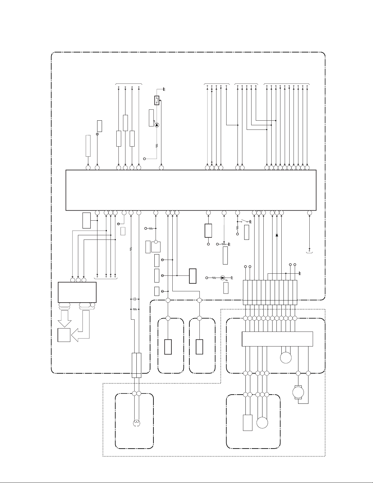
SCHEMATIC DIAGRAMS / CBA’S AND TEST POINTS
Standard Notes
WARNING
Many electrical and mechanical parts in this chassis
have special characteristics. These characteristics
often pass unnoticed and the protection afforded by
them cannot necessarily be obtained by using
replacement components rated for higher voltage,
wattage, etc. Replacement parts that have these
special safety characteristics are identified in this
manual and its supplements; electrical components
having such features are identified by the mark “#” in
the schematic diagram and the parts list. Before
replacing any of these components, read the parts list
in this manual carefully. The use of substitute
replacement parts that do not have the same safety
characteristics as specified in the parts list may create
shock, fire, or other hazards.
Notes:
1. Do not use the part number shown on these
drawings for ordering. The correct part number is
shown in the parts list, and may be slightly
different or amended since these drawings were
prepared.
2. All resistance values are indicated in ohms
(K = 10
3. Resistor wattages are 1/4W or 1/6W unless
otherwise specified.
4. All capacitance values are indicated in µF
(P = 10
5. All voltages are DC voltages unless otherwise
specified.
3
, M = 106).
-6
µF).
1-13-1 T2N_SC
Page 38

LIST OF CAUTION, NOTES, AND SYMBOLS USED IN THE SCHEMATIC DIAGRAMS ON
THE FOLLOWING PAGES:
1. CAUTION:
FOR CONTINUED PROTECTION AGAINST FIRE HAZARD, REPLACE ONLY WITH THE
F
A V
SAME TYPE FUSE.
ATTENTION: POUR UNE PROTECTION CONTINUE LES RISQES D'INCELE N'UTILISER
QUE DES FUSIBLE DE MÊME TYPE.
RISK OF FIRE-REPLACE FUSE AS MARKED.
This symbol means fast operating fuse.
Ce symbole represente un fusible a fusion rapide.
2. CAUTION:
Fixed Voltage (or Auto voltage selectable) power supply circuit is used in this unit.
If Main Fuse (F2001) is blown, first check to see that all components in the power supply circuit are not
defective before you connect the AC plug to the AC power supply. Otherwise it may cause some components
in the power supply circuit to fail.
3. Note:
1. Do not use the part number shown on the drawings for ordering. The correct part number is shown in the
parts list, and may be slightly different or amended since the drawings were prepared.
2. To maintain original function and reliability of repaired units, use only original replacement parts which are
listed with their part numbers in the parts list section of the service manual.
4. Mode: SP/REC
5. Voltage indications for PLAY and REC modes on the schematics are as shown below:
< DVD/HDD Section >
5.0
The same voltage for
both PLAY & STOP modes
5.0
(2.5)
PLAY mode
STOP mode
231
Indicates that the voltage
is not consistent here.
The same voltage for
both PLAY, REC & DVD
modes
< VCR Section >
231
5.0
5.0
(2.5)
< >
Indicates that the voltage
is not consistent here.
PLAY mode
REC mode
DVD mode
Unit: Volts
6. How to read converged lines
1-D3
Distinction Area
Line Number
(1 to 3 digits)
3
1-B1
AREA D3
2
AREA B1
Examples:
1. "1-D3" means that line number "1" goes to the line number
"1" of the area "D3".
1
1-D3
2. "1-B1" means that line number "1" goes to the line number
"1" of the area "B1".
ABCD
7. Test Point Information
: Indicates a test point with a jumper wire across a hole in the PCB.
: Used to indicate a test point with a component lead on foil side.
: Used to indicate a test point with no test pin.
: Used to indicate a test point with a test pin.
1-13-2 T2N_SC
Page 39

AV 1/8 Schematic Diagram < VCR Section >
AV 1/8
Ref No. Position
IC4501 C-3
Q4501 E-1
Q4502 E-2
Q4506 A-2
Q4508 C-1
Q4509 C-1
Q4510 C-1
CN4501 A-4
CN4502 F-4
CN4504 A-4
VR4501 B-3
TP4508 A-2
TP4513 B-4
IC
CONNECTORS
TRANSISTORS
VARIABLE RESISTOR
TEST POINTS
1-13-3
E4340SCAV1
Page 40

AV 2/8 & Sensor Schematic Diagram < VCR Section >
5G 4G 3G 2G 1G
7G
6G
TIME
P-SCAN
DB
C
SHIFT
VCR
HDD
DVD
PM
CD
R
W
a
b
c
d
d
ef
f
h
h
h
g
C
TIME
SHIFT
7G 6G 5G 4G 3G 2G 1G
a
b
c
d
e
f
g
c
d
e
ff
g
c
d
e
f
g
c
d
e
f
g
c
d
e
f
g
c
d
e
f
g
hh h
d
f
h
i
a
b
c
d
e
g
a
b
abababa
b
FL4502 MATRIX CHART
CD
P-SCAN
DVD
PM
HDD
VCRDB
R
W
AV 2/8
Ref No. Position
IC4571 J-3
Q4561 G-1
TP4502 H-4
TP4506 K-1
TP4507 K-1
IC
TRANSISTOR
TEST POINTS
1-13-4
E4340SCAV2
Page 41

AV 3/8 Schematic Diagram < VCR Section >
AV 3/8
Ref No. Position
IC4301 N-2
Q4301 Q-3
Q4302 Q-4
Q4303 Q-4
Q4421 N-1
Q4422 N-1
Q4425 N-1
Q4426 N-1
CN4253 M-4
TP4301 P-1
TP4302 O-4
IC
TEST POINTS
TRANSISTORS
CONNECTOR
1-13-5
E4340SCAV3
Page 42

AV 4/8 Schematic Diagram < VCR Section >
AV 4/8
Ref No. Position
IC4451 S-2
TP4452 V-3
IC
TEST POINT
1-13-6
E4340SCAV4
Page 43

AV 5/8 Schematic Diagram < VCR Section >
AV 5/8
Ref No. Position
IC4003 Z-4
IC4005 Z-2
IC4006 AA-2
IC4007 BB-2
Q4004 AA-2
Q4005 AA-1
Q4006 BB-1
Q4025 AA-1
CN4001 CC-3
CN4002 X-2
CONNECTORS
TRANSISTORS
ICS
1-13-7
E4340SCAV5
Page 44

AV 6/8 Schematic Diagram < VCR Section >
AV 6/8
Ref No. Position
IC4008 EE-2
IC4009 FF-4
IC4010 FF-4
IC4011 EE-1
Q4013 GG-2
Q4020 FF-1
Q4021 FF-1
Q4022 FF-1
Q4023 GG-1
JP4015 HH-4
JP4016 HH-4
JP4017 HH-4
TRANSISTORS
TEST POINTS
ICS
1-13-8
E4340SCAV6
Page 45

AV 7/8 & Power SW Schematic Diagram < VCR Section >
*1 NOTE
IC4002
BU4219G-TR
PST3619NR
Group A Group B
C4174 0.015 0.1
These components (IC4002, C4174)
can be used in any models.
However, you cannot mix components under
Group A with the ones under Group B.
You can choose either Group. The difference
between Group A and Group B is shown below.
AV 7/8
Ref No. Position
IC4001 LL-2
IC4002 MM-1
Q4001 KK-1
Q4002 NN-3
Q4003 NN-3
CN4004 JJ-4
CN4005 KK-1
ICS
TRANSISTORS
CONNECTORS
1-13-9
E4340SCAV7
Page 46

AV 8/8 Schematic Diagram < VCR Section >
AV 8/8
Ref No. Position
IC4251 QQ-3
Q4251 QQ-3
Q4252 RR-3
Q4256 SS-4
Q4257 RR-2
Q4258 SS-2
Q4264 TT-3
CN4251 PP-3
CONNECTOR
IC
TRANSISTORS
1-13-10
E4340SCAV8
Page 47

Power Supply Schematic Diagram < VCR Section >
POWER SUPPLY
Ref No. Position
IC2101 B-1
IC2201 C-1
IC2204 D-2
IC2401 D-4
IC2402 D-4
Q2101 A-3
Q2102 A-2
Q2203 D-3
Q2204 C-2
Q2205 D-2
Q2209 C-1
Q2214 E-2
Q2215 E-3
Q2221 C-2
Q2226 D-2
Q2227 D-1
Q2228 D-2
Q2338 D-3
Q2339 E-2
Q2341 E-1
Q2415 E-3
CN2201 F-4
CN2202 F-2
CN2203 F-3
CN2204 F-3
TRANSISTORS
IC
CONNECTORS
CAUTION !
Fixed voltage (or Auto voltage selectable) power supply circuit is used in this unit.
If Main Fuse (F2001) is blown , check to see that all components in the power supply
circuit are not defective before you connect the AC plug to the AC power supply.
Otherwise it may cause some components in the power supply circuit to fail.
F
A V
CAUTION !
For continued protection against fire hazard,
replace only with the same type fuse.
ATTENTION : Pour une protection continue les risqes
d'Incele n'utiliser que des fusible de même type.
Risk of fire-replace fuse as marked.
"This symbol means fast operating fuse."
"Ce symbole reprèsente un fusible à fusion rapide."
NOTE:
The voltage for parts in hot circuit is measured using
hot GND as a common terminal.
1-13-11
E4340SCP
Page 48

Front Jack & Open/Close Schematic Diagram < VCR Section >
FRONT JACK
Ref No. Position
Q2501 A-3
Q2502 A-3
Q2503 B-3
Q2504 B-3
Q2505 B-3
Q2506 D-2
CN2501 E-3
CN2502 D-1
CONNECTORS
TRANSISTORS
ATA Schematic Diagram < DVD/HDD Section >
1-13-12
E4340SCJ
E4340SCAT
Page 49

DVD/HDD Main 1/6 Schematic Diagram < DVD/HDD Section >
DVD/HDD MAIN 1/6
Ref No. Position
IC101 C-3
IC102 B-4
Q402 B-1
Q403 C-1
CN101 A-3
CONNECTOR
TRANSISTORS
ICS
1-13-13
E4340SCM1
Page 50

DVD/HDD Main 2/6 Schematic Diagram < DVD/HDD Section >
DVD/HDD MAIN 2/6
Ref No. Position
IC201 H-4
CN201 L-2
IC
CONNECTOR
1-13-14
E4340SCM2
Page 51

DVD/HDD Main 3/6 Schematic Diagram < DVD/HDD Section >
DVD/HDD MAIN 3/6
Ref No. Position
IC202 Q-2
IC204 P-4
IC401 N-2
IC402 P-2
IC410 Q-3
CN202 R-4
CN401 M-2
ICS
CONNECTORS
1-13-15
E4340SCM3
Page 52

DVD/HDD Main 4/6 Schematic Diagram < DVD/HDD Section >
DVD/HDD MAIN 4/6
Ref No. Position
IC601(1/6) T-4
IC601(2/6) S-2
IC901 U-2
IC902 V-3
Q801 S-3
Q802 S-3
CN501 X-4
CN601 X-2
ICS
CONNECTORS
TRANSISTORS
NOTE:
1. The order of pins shown in this diagram is different from that of actual IC601.
2. IC601 is divided into six and shown as IC601 (1/6) ~ IC601 (6/6) in this DVD/HDD Main Schematic Diagram Section.
1-13-16
E4340SCM4
Page 53

DVD/HDD Main 5/6 Schematic Diagram < DVD/HDD Section >
DVD/HDD MAIN 5/6
Ref No. Position
IC601(3/6) BB-4
IC601(4/6) BB-1
IC604 Z-4
IC605 Z-2
CN602 DD-1
CONNECTOR
ICS
NOTE:
1. The order of pins shown in this diagram is different from that of actual IC601.
2. IC601 is divided into six and shown as IC601 (1/6) ~ IC601 (6/6) in this DVD/HDD Main Schematic Diagram Section.
1-13-17
E4340SCM5
Page 54

DVD/HDD Main 6/6 Schematic Diagram < DVD/HDD Section >
DVD/HDD MAIN 6/6
Ref No. Position
IC501 II-1
IC601(5/6) GG-4
IC601(6/6) II-4
IC602 FF-2
IC603 FF-4
ICS
NOTE:
1. The order of pins shown in this diagram is different from that of actual IC601.
2. IC601 is divided into six and shown as IC601 (1/6) ~ IC601 (6/6) in this DVD/HDD Main Schematic Diagram Section.
1-13-18
E4340SCM6
Page 55

AV CBA Top View
AV CBA
Ref No. Position Ref No. Position
IC4001 D-2 Q4303 B-3
IC4002 D-2 Q4421 C-3
IC4003 E-4 Q4422 C-3
IC4005 F-2 Q4425 C-3
IC4006 E-3 Q4426 C-2
IC4007 E-2 Q4501 A-4
IC4008 E-3 Q4502 B-4
IC4009 F-3 Q4506 B-3
IC4010
F-3
Q4508
B-2
IC4011 E-4 Q4509 B-2
IC4251 E-1 Q4510 B-2
IC4301 C-3 Q4561 A-3
IC4451 B-4
IC4501 A-4 CN4001 D-1
IC4571 A-2 CN4002 B-1
CN4004 F-1
Q4001 B-4 CN4005 B-5
Q4002 D-3 CN4251 F-1
Q4003 D-3 CN4253 C-4
Q4004 E-2 CN4501 C-5
Q4005 E-2 CN4502 B-1
Q4006 E-1 CN4504 C-2
Q4013 E-4
Q4020 F-2 VR4501 B-5
Q4021 F-2
Q4022 F-2 JP4015 F-4
Q4023
F-1
JP4016
F-4
Q4025 E-2 JP4017 F-4
Q4251 E-1 TP4301 B-5
Q4252 E-1 TP4302 D-4
Q4256 F-1 TP4452 C-5
Q4257 F-1 TP4502 B-1
Q4258 F-2 TP4506 B-1
Q4264 C-1 TP4507 B-5
Q4301 B-3 TP4508 B-4
Q4302
B-3
TP4513
D-4
TEST POINTS
TRANSISTORSICS
CONNECTORS
TRANSISTORS
VARIABLE RESISTOR
WF3
TP4301
C-PB
TO SENSOR CBA
(END-SENSOR)
WF2
TP4302
RF-SW
Sensor CBA Top View
TP4513
CTL
BHB300F01011A
BHB300F01011B
WF1
JP4017
V-OUT
TP4502
S-INH
TO SENSOR CBA (START-SENSOR)
1-13-19
BE4340F01044A
Page 56

AV CBA Bottom View
WF6
PIN 2 OF
IC4008
WF13
PIN 17 OF
TU4001
WF8
PIN 3 OF
CN4001
WF7
PIN 5 OF
CN4001
WF4
PIN 7 OF
CN4001
WF5
PIN 9 OF
CN4001
WF9
PIN 17 OF
CN4001
WF10
PIN 1 OF
CN4251
1-13-20
BE4340F01044A
Page 57

Power Supply CBA Top View
Because a hot chassis ground is present in the power
supply circut, an isolation transformer must be used.
Also, in order to have the ability to increase the input
slowly, when troubleshooting this type power supply
circuit, a variable isolation transformer is required.
F
A V
CAUTION !
For continued protection against fire hazard,
replace only with the same type fuse.
ATTENTION : Pour une protection continue les risqes
d'Incele n'utiliser que des fusible de même type.
Risk of fire-replace fuse as marked.
"This symbol means fast operating fuse."
"Ce symbole reprèsente un fusible à fusion rapide."
CAUTION !
Fixed voltage (or Auto voltage selectable) power supply circuit is used in this unit.
If Main Fuse (F2001) is blown , check to see that all components in the power supply
circuit are not defective before you connect the AC plug to the AC power supply.
Otherwise it may cause some components in the power supply circuit to fail.
NOTE:
The voltage for parts in hot circuit is measured using
hot GND as a common terminal.
POWER SUPPLY
Ref No. Position
IC
IC2101 C-4
IC2201 B-4
IC2204 B-1
IC2401 C-1
IC2402 C-1
TRANSISTORS
Q2101 C-2
Q2102 C-3
Q2203 B-1
Q2204 A-2
Q2205 A-2
Q2209 B-4
Q2214 B-2
Q2215 A-4
Q2221 A-1
Q2226 C-2
Q2227 C-1
Q2228 C-1
Q2338 A-4
Q2339 B-1
Q2341 B-1
Q2415 C-1
CONNECTORS
CN2201 C-1
CN2202 A-3
CN2203 A-1
CN2204 A-4
1-13-21
BE4340F01024A
Page 58

Power Supply CBA Bottom View
Because a hot chassis ground is present in the power
supply circut, an isolation transformer must be used.
Also, in order to have the ability to increase the input
slowly, when troubleshooting this type power supply
circuit, a variable isolation transformer is required.
F
A V
CAUTION !
For continued protection against fire hazard,
replace only with the same type fuse.
ATTENTION : Pour une protection continue les risqes
d'Incele n'utiliser que des fusible de même type.
Risk of fire-replace fuse as marked.
"This symbol means fast operating fuse."
"Ce symbole reprèsente un fusible à fusion rapide."
CAUTION !
Fixed voltage (or Auto voltage selectable) power supply circuit is used in this unit.
If Main Fuse (F2001) is blown , check to see that all components in the power supply
circuit are not defective before you connect the AC plug to the AC power supply.
Otherwise it may cause some components in the power supply circuit to fail.
NOTE:
The voltage for parts in hot circuit is measured using
hot GND as a common terminal.
1-13-22
BE4340F01024A
Page 59

Power SW CBA Top View Power SW CBA Bottom View
BE4340F01044B
Open/Close CBA Top View Open/Close CBA Bottom View
ATA CBA Top View ATA CBA Bottom View
BE4340F01024C
BE4340F01031
1-13-23
Page 60

Front Jack CBA Top View
FRONT JACK
Ref No. Position
Q2501 B-1
Q2502 B-1
Q2503 B-1
Q2504 A-1
Q2505 A-1
Q2506 B-1
CN2501 B-1
CN2502 B-1
TRANSISTORS
CONNECTORS
Front Jack CBA Bottom View
1-13-24
BE4340F01024B
Page 61

WAVEFORMS
NOTE:
Input: COLOR BAR SIGNAL (WITH 1KHz AUDIO SIGNAL)
JP4017
WF1
WF5
Pin 9 of CN4001
WF9
Pin 17 of CN4001
V-OUT E-E 0.2V 20
WF1
WF2
WF3
WF2
UPPER
UPPER
JP4017
LOWER
TP4302
V-OUT 0.5V
RF-SW 5V
TP4301
LOWER
TP4302
µs
50
µs
VIDEO-C 0.2V 20µs
WF6
Pin 2 of IC4008
VIDEO-CVBS 0.5V 20µs
WF7
Pin 5 of CN4001
AUDIO(L)-OUT
WF10
Pin 1 of CN4251
SPDIF 1V 0.1µs
WF13
Pin 17 of TU4001
1V 0.5ms
C-PB
RF-SW 5V 5m
WF4
Pin 7 of CN4001
VIDEO-Y 0.2V 20µs
0.2V
s
VIDEO-Cb
WF8
Pin 3 of CN4001
VIDEO-Cr
0.2V 20µs
0.2V 20µs
1-14-1
0.5V 0.2msTU VIDEO 0.2V 20
E4340WF
µs
Page 62

Wiring 1/2 Diagram
TO
1
2NU3
4
5
6
8
9
10
11
12
GND
SPDIF
CN4251
FAN-LOCK
FAN-CONT1
LOW-POW
REG-CONT
PWR-SW
SAFETY17SAFETY2
GND
P-ON+5V(A)
POWER
SUPPLY CBA
CN2202
(W3)
13
AL+5V(2)14AL+5V(2)15AL+5V(1)
P-ON+5V(A)
WIRING DIAGRAMS
TO WIRING 2/2
DIAGRAM
16
GND17GND18GND
19
20
21
AL+44V
P-ON+9V
23NU24NU25
AL+12V22AL+12V
27
GND26GND
28F129F230
AL-24V
1
CN4001
VIDEO-Y(I)
GND 2
GND 4
VIDEO-Cr/Pr 3
TO
DVD/HDD
MAIN CBA
CN601
(W1)
15
17
19
21
GND 16
GND 12
GND 10
GND 6
GND 8
VIDEO-C 9
VIDEO-Y(I/P) 7
VIDEO-Cb/Pb 5
GND 14
GND 18
GND 22
AUDIO(L)-IN 13
AUDIO(R)-IN 11
AUDIO(R)-OUT
AUDIO+5V 20
AUDIO(L)-OUT
DVD/HDD-A-MUTE
VIDEO-Y/CVBS
27
29
VJ 26
RDY 28
GND 24
VIDEO-C 23
SUB-TXD
SUB-RXD
SUB-SCLK 25
SYS-RESET 30
REAR
ANT-IN ANT-OUT
DIGITAL
AUDIO
AUDIO(R)
-OUT1
AUDIO(L)
-OUT1
VIDEO-
Cr/Pr
VIDEO-
Cb/Pb
VIDEO-Y
OUT
AUDIO(R)
-IN1
AUDIO(L)
-IN1
VIDEO
-IN1
AUDIO(R)
-OUT2
AUDIO(L)
-OUT2
VIDEO
OUT
OUT
OUT
OUT
AV CBA
SENSOR CBA
FE-H
FE-H GND
CN4501
1
2
SENSOR CBA
CN4006
W6
CN4005
CN4502
S-VIDEO
IN2
POWER SW CBA
1
CN2501
W4
POWER-LED
AL+5V(3)
GND
SUB-KEY-1
11
44
33
2 2
C-F/R
C-FG
C-CONT
AL+12V(CAP)
1
P-ON+5V(1)
2
4
3
GND
5
6
CN4002
GND
D-CONT9D-PFG
LM-FWD/REV
8
7
10
SUB-KEY-1
1
AL+12V
11
FRONT
VIDEO
-IN2
AUDIO(R)
-IN2
5
3
4
6
2
DUBBUNG-LED
HDD-LED
AL+5V(3)
VCR-LED
DVD-LED
5
3
4
6
2
AL+18V
12
AUDIO(L)
-IN2
FRONT
JACK CBA
8
9
7
10
DVD-REC-LED
GND
SUB-KEY-2
HDD-REC-LED
8
9
7
10
11
12
RESET
C-IN2
11
12
CN4253
VIDEO(R)-1
1
1
CN2503
W7
SUB-KEY-2
1
CN2502
13
14
15
GND
Y-IN2
GND
13
14
15
VIDEO(L)-1
VIDEO(L)-2
VIDEO-COM
2
4
3
OPEN/CLOSE
CBA
3
2
4
SUB-KEY-1
GND
AL+5V
3
2
4
16
17
18
VIDEO-IN2
GND
AUDIO(L)-IN2
16
17
18
VIDEO-COM
VIDEO(R)-2
Hi-Fi-AUDIO(R)
7
5
6
5
DUBBUNG-LED
5
19
20
GND
AUDIO(R)-IN2
19
20
Hi-Fi-AUDIO(L)
Hi-Fi-COM
8
9
S-VIDEO
IN1
S-VIDEO
OUT
(DECK ASSEMBLY)
CN4504
AE-H
1
AUDIO
ERASE
AC HEAD
ASSEMBLY
AUDIO-PB/REC
CTL(+)
AE-H/FE-H
A-COM
23456
HEAD
HEAD
AUDIO
CONTROL
CTL(-)
HEAD
FE HEAD
FULL
ERASE
CAPSTAN
MOTOR
HEAD
M
LOADING
MOTOR
M
MOTOR
DRIVE
CIRCUIT
PG
SENSOR
CYLINDER
ASSEMBLY
M
DRUM
MOTOR
CAPSTAN
MOTOR
VIDEO
(R)1
HEAD
VIDEO
(L)1
HEAD
VIDEO
(L)2
HEAD
VIDEO
(R)2
HEAD
Hi-Fi
AUDIO
(R) HEAD
Hi-Fi
E4340WI11-15-1
AUDIO
(L) HEAD
Page 63

Wiring 2/2 Diagram
SPDIF 1
CN2202
NU 3
FAN-LOCK 4
REG-CONT 5
FAN-CONT1 2
GND 10
GND 11
PWR-SW 9
SAFETY1 7
SAFETY2 8
LOW-POW 6
P-ON+5V(A) 12
AL+5V(2) 14
P-ON+5V(A) 13
TO WIRING 1/2
DIAGRAM
TO AV CBA
CN4251
(W3)
GND 17
GND 18
AL+5V(2) 15
AL+5V(1) 16
FAN
W8
2
F1 29
NU 24
GND 19
AL+44V 20
NU 25
GND 26
AL+12V 22
AL+12V 23
P-ON+9V 21
F2 30
GND 27
AL-24V 28
FAN 1
CN2204
CN2203
FAN-LOCK
HDD+5V 1
HDD+12V 4
GND 2
GND 3
AC CORD
CN2201
SPDIF1
W2
CN501
SPDIF 1
GND2
EV+10.5V4
EV+10.5V5
GND3
EV+10.5V6
GND7
GND8
GND9
GND10
P-ON+5V11
P-ON+5V12
P-ON+5V13
EV+2.4V14
EV+2.4V15
EV+2.4V16
EV+2.4V17
GND18
GND19
P-ON+2.5V20
P-ON+2.5V21
P-ON+2.5V22
GND23
GND24
P-ON+3.3V25
P-ON+3.3V26
P-ON+3.3V27
GND28
GND29
GND30
CN601
GND 2
EV+10.5V 4
EV+10.5V 5
EV+10.5V 6
GND 7
GND 8
GND 9
GND 10
P-ON+5V 11
P-ON+5V 12
P-ON+5V 13
EV+2.4V 14
EV+2.4V 15
EV+2.4V 16
EV+2.4V 17
GND 3
GND 18
GND 19
P-ON+2.5V 20
P-ON+2.5V 21
P-ON+2.5V 22
GND 23
GND 24
P-ON+3.3V 25
P-ON+3.3V 26
1245678
1245678
W5
P-ON+3.3V 27
GND 28
GND 29
GND 30
VIDEO-Y(I) 1
GND 2
VIDEO-Cr/Pr 3
GND 4
VIDEO-Cb/Pb 5
9
1011121314151617183192021222324252627282930313233343536373839
9
1011121314151617183192021222324252627282930313233343536373839
POWER SUPPLY CBA
GND 10
VIDEO-C 9
GND 6
VIDEO-Y(I/P) 7
GND 8
HARD
DISK
ATA
CBA
AUDIO(R)-IN 11
GND 12
DRIVE
AUDIO(L)-IN 13
GND 14
TO WIRING 1/2
DIAGRAM
TO AV CBA
CN4001
(W1)
15
17
GND 16
AUDIO(R)-OUT
AUDIO(L)-OUT
GND 18
19
21
DVD/HDD-A-MUTE
AUDIO+5V 20
VIDEO-Y/CVBS
GND 22
VIDEO-C 23
GND 24
SUB-SCLK 25
VJ 26
SUB-TXD27RDY 28MSUB-RXD29SYS-RESET 30
40
40
DVD/HDD MAIN CBA
NRESET 1
GND 2
HDD8 4
HDD6 5
HDD9 6
HDD5 7
HDD10 8
HDD4 9
HDD11 10
HDD3 11
HDD12 12
HDD2 13
HDD13 14
HDD1 15
HDD14 16
HDD0 17
HDD7 3
HDD15 18
GND 19
NU 20
DMARQ 21
GND 22
NIOWR 23
GND 24
NIORD 25
GND 26
IORDY 27
NU 28
NDMACK 29
GND 30
INTRQ 31
NIOCS16 32
DA1 33
NPDIGA 34
DA0 35
DA2 36
NCS1FX 37
NCS3FX 38
NDASP 39
GND 40
118
217
415
316
CN401
VH-
HW-
HV-
HW+
CN1001
123
CN1003
SLED
SENSOR
DVD MECHANISM
DVD MECHANISM & DVD/HDD MAIN CBA ASSEMBLY
910 U
514
613
712
811
109
HV+
HU-
HU+
VCC
V
RELAY
CBA
OPEN
TRAY
ENCODER CBA
118W127
136
145
154
T-SCN3
T-SCN2
GND
SL+
~
1
CN1002
11
LOADER CBA
SPINDLE
MOTOR
163
SL-
172
SW1
M
SLED
MOTOR
CN101 CN3001CN201 CN3002
FCS(+) 4TRK(-)
TRK(+)
1
3
2 FCS(-)
FOCUS
ACTUATOR
TRACKING
PICKUP
6 TILT(-)
5 TILT(+)
ACTUATOR
TILT
ACTUATOR
FPD
GND9GND11FPD-SW
THERMO
7
VC-FPD
8
10
12
FPDIC
1-15-2
VC-PD15H16D17C18F19NU20NU21SW22RF(+)23RF(-)24E25B26A27G28GND29VCC230IIN331IIN232IIN133GND34XOUTEN335GND36XOUTEN237GND38OSCEN39LDEN240LDEN1
VCC1
14
13
PDIC
DVD-LD
DVD/CD
LASER
DIODE
DRIVE
CD-LD
E4340WI2
Page 64

SYSTEM CONTROL TIMING CHARTS
< VCR Section >
Mode SW: LD-SW
LD-SW Position detection
A/D Input voltage Limit
(Calculated voltage)
3.76 V ~ 4.50 V (4.12 V) EJ
4.51 V ~ 5.00 V (5.00 V) CL
0.00 V ~ 0.25 V (0.00 V) SB
1.06 V ~ 1.50 V (1.21 V) TL
0.66 V ~ 1.05 V (0.91 V) FB
1.99 V ~ 2.60 V (2.17 V) SF
1.51 V ~ 1.98 V (1.80 V) SM
3.20 V ~ 3.75 V (3.40 V) AU
0.26 V ~ 0.65 V (0.44 V) AL
4.51 V ~ 5.00 V (5.00 V) SS
Symbol
2.61 V ~ 3.19 V (2.97 V) RS
Note:
Note: EJ RS: Loading FWD (LM-FWD / REV “H”)
RS EJ: Loading REV (LM-FWD / REV “L”)
Stop (A) = Loading
Stop (B) = Unloading
Note:
Symbol Loading Status
EJ Eject
CL Eject ~ REW Reel
SB REW Reel ~ Stop (B)
TL Stop (B) ~ Brake Cancel
FB Brake Cancel ~ FF / REW
SF FF / REW ~ Stop (M), (FF / REW)
SM Stop (M), (FF / REW) ~ Stop (A)
AU Stop (A) ~ Play / REC
AL Play / REC ~ Still / Slow
SS Still / Slow ~ RS (REW Search)
RS RS (REW Search)
1-16-1 T2N4HTI
Page 65

Still/Slow Control Frame Advance Timing Chart
1) SP Mode
18 RF-SW
The first rise of RF-SW after a rise in F-AD signal
F-AD
(Internal Signal)
C-DRIVE
PB CTL
27 C-F/R
AT
"L" "L"
"H"
Acceleration Detection (T1)
"Z"
ST
"H"
Stop detection (T2)
Slow Tracking Value
BL
20ms
Reversal Limit Value
79 H-A-SW
78 C-ROTA
STILL FRAME ADVANCE STILL
Fig. 1
1-16-2 T2N4HTI
Page 66

2) LP/SLP Mode
18 RF-SW
F-AD
(Internal Signal)
The first rise of RF-SW after a rise in F-AD signal
AT
C-DRIVE
PB CTL
27 C-F/R
"H"
"L" "L"
Acceleration Detection (T1)
"Z"
ST
"H"
Stop detection (T2)
Slow Tracking Value
BL
20ms
Reversal Limit Value
79 H-A-SW
78 C-ROTA
STILL STILL
FRAME ADVANCE
Fig. 2
1-16-3 T2N4HTI
Page 67

LM-FWD "M"
/REV
21
CL/SS
EJ
AU
RS
SF
SM
TL
FB
AL
SB
68
LD-SW
PIN NO.
1. EJECT (POWER OFF) -> CASSETTE IN (POWER ON) -> STOP(B) -> STOP(A) -> PLAY -> RS -> FS -> PLAY -> STILL -> PLAY -> STOP(A)
ROTATION
DRUM
27
C-F/R
C-DRIVE
22
24
VCR/TV
DISPLAY
D-REC-H
D-PB
26
P-ON-L
A-MUTE-H
-OFF
POWER
STOP
PLAY RS
0.1S
0.2S
1.5S (2H)
2.5S (4H)
0.2S
0.8S
0.3S
ON
0.2S
ON
0.2S
40mS
1.2S
0.2S
0.4S
20mS
"Z"
0.2S
0.2S
0.2S
0.2S
TL
SF
AU
AU
AU
CLEJ
SB
TL SB
FB
SM
SM
SMSF AL AL RS AU AL SS AU AL SM
EJECT
CASS.LOAD
LD-FWD
0.2S
LD-REV
0.7S
LD-FWD
0.4S
LD-FWD
0.2S
LD-REV
0.2S
LD-FWD
0.5S
LD-REV
STOP(A)
LD-FWD
PLAY
ST-S/
END-S
"OFF"
PLAY
(SLOW)
FS
PLAY STOPPLAY
STILL
0.2S
1.0S
0.5S
0.8S (2H)
1.2S (4H)
40mS
Refer to STILL/
SLOW TIMING
CHART Fig. 1, 2.
0.4S
20mS
Fig. 3
0.2S
0.3S
0.3S
SS
AL
AL
SS
AU
LD-FWD
RS
LD-REV
0.2S
LD-FWD
FS
PLAY
LD-FWD
STILL(SLOW)
LD-REV
0.2S
LD-FWD
PLAY
LD-REV
STOP(A)
REW
FF
PLAY
PAUSE
(SLOW)
PLAY
STOP
/EJECT
1-16-4 T2N4HTI
Page 68

LM-FWD "M"
/REV
26
CL/SS
EJ
AU
RS
SF
SM
TL
FB
AL
SB
87
LD-SW
PIN NO.
2. STOP(A) -> FF -> STOP(A) -> REW -> STOP(A) -> REC -> PAUSE -> PAUSE or REC -> STOP(A) -> EJECT
DRUM
ROTATION
27
29
D-REC-H
VCR/TV97
DISPLAY
D-PB
31
A-MUTE-H
P-ON-L
32
C-F/R
C-DRIVE
STOP
STOPFF
REW STOP
REC
RECREC PAUSE STOP
1.0S
1.2S
ON
ON
40mS
40mS
40mS
0.4S
0.4S
0.4S
20mS
20mS
"Z"
0.2S
0.2S
0.2S
0.2S
0.2S
SM SF FB SM AU AU SS
FB SF AU AUFB SF
TL TL SMSM SF SFAL AL SM AL AL ALAU AU SM TL SB EJRS RSSM
SF FB SM
AU
SS SS SF
AL AL AUSS FB CL
STOP(A)
LD-REV
0.2S
LD-FWD
FF
REV
1.0S
LD-FWD
0.5S
LD-REV
STOP(A)
LD-REV
0.2S
LD-FWD
REW
LD-REV
1.0S
LD-FWD
0.5S
LD-REV
STOP(A)
LD-FWD
REC
LD-FWD
2.5S Short REV
LD-REV
0.2S
LD-FWD
REC PAUSE
REC
LD-FWD
1.5S
LD-REV
0.2S
LD-FWD
0.5S
LD-REV
FF
STOP
/EJECT
REW
STOP
/EJECT
REC
PAUSE
REC or
PAUSE
STOP
/EJECT
20mS
0.1S
0.2S
STOP(A)
LD-REV
0.2S
LD-REV
0.5S
0.2S
0.5S
CASS. UNLD
EJECT
STOP
/EJECT
ST-S/
END-S
"ON"
Fig. 4
1-16-5 T2N4HTI
Page 69

< DVD/HDD Section >
Ye s
No
Is Timer
ET1 passed?
Case 1
No
Power on
INNER-SW
open?
No
Rezero 1
INNER-SW
open?
Ye s
To disc
distintion
Case 2
Ye s
Rezero 2
[ Tray Open ]
button is pressed.
[ Tray Open ]
button is pressed.
Tray insertion
Is slit S5
passed?
Is Timer
ET4 passed?
INNER-SW
No
open?
Case 3
[ open ] button is pressed.
No
Ye s
Case 4
[ open ] button is pressed.
Ye s
No
Ye s
Push Close
No
Is Timer
ET3 passed?
Ye s
No
Tray ejection
Is slit S1
passed?
Ye s
Is Timer
ET2 passed?
No
Is not
slit passed?
Ye s
Tray ejection
completion
No
Ye s
No
Is Timer
ET1 passed?
Ye s
Case 5
Retry.
Retry OK?
Ye s
In case of "No" by the 6th time retry.
No
Tray insertion
1-16-6 T2N4HTI
Page 70

Parameter
Tray open
V*: Voltage (HEX)
S*: Encoder pulse
(HEX)
T*: Event timer
ET*: Error
detection timer
V0: 2.0 V (00d) S1: 300 (12c) T1: 0.1 s ET1: 5.0 s
V1: 4.5 V (022) S2: 3300 (ce4) T2: 3.0 s ET2: 5.0 s
V2: 2.2 V (010) S3: 3935 (f5f) T3: 3.0 s ET3: 3.0 s
V3: 2.4 V (013) S4: 0 (000) T4: 0.1 s ET4: 3.0 s
V4: 6.0 V (030) S5: 3000 (bb8) T5: 0.1 s
Encoder pulse
S3
S2
S1
Tray ejection direction
SLED
Tray insersion direction
open
INNER-SW
close
Timer ET1
ET2
T1
V0
V2
V1
1-16-7 T2N4HTI
Page 71

Tray close
Push close
Tray ejection direction
SLED
Tray insersion direction
open
INNER-SW
close
Timer
S5
S4
ET3 ET4
S5
Push Close
V3
V4
Encoder pulse
SLED
Tray insersion direction
open
INNER-SW
close
Timer
T3
V3
V4
ET4
1-16-8 T2N4HTI
Page 72

Case 1
Case 2
SLED
Tray insersion direction
open
INNER-SW
close
Timer
T2
Rezero 1
V3
V4
ET4
Tray ejection direction
SLED
Tray insersion direction
open
INNER-SW
close
Rezero 2
V0V0
Case 3 (When [OPEN] button is pressed before the S5 passage.)
Encoder pulse
Tray ejection direction
SLED
V2
Timer
T1
Case 4 (When [OPEN] button is pressed after the S5 passage.)
It starts opening after making closing complete once.
1-16-9 T2N4HTI
Page 73

Case 5 (Retry.)
S1
Tray ejection direction
SLED
Tray insersion direction
open
INNER-SW
close
Retry frequency V1+
1st time retry 6 v
2nd time retry 7 v
3rd time retry 8 v
4th time retry 9 v
5th time retry 9 v
6th time retry 9 v
V1+
V26v
Start retry.
1-16-10 T2N4HTI
Page 74

IC PIN FUNCTION DESCRIPTIONS
< VCR Section >
IC4501 (MICROCONTROLLER)
“H” ≥ 4.5 V, “L” ≤ 1.0 V
Pin
No.
IN/
OUT
1INS-CS
2IN
3INT-REEL
4-NU
5IN
6INS-CLOCK
7INS-DATA-IN
8OUT
9OUT
10 OUT
11 OUT
IN/
12
OUT
13 OUT
14 OUT YCA-SCL YCA IC Control Clock
15 OUT YCA-SDA YCA IC Control Data
16 OUT YCA-CS YCA IC Control Chip Select
17 - NU
18 OUT RF-SW
19 OUT D-V SYNC
20 IN RESET
21 OUT
22 OUT P-ON-L
23 - NU
Signal
Name
REC-SAFSW
REMOTEVIDEO
S-DATAOUT
DISPLAYENA
DISPLAYDATA
DISPLAYCLK
IIC-BUS
SDA
IIC-BUS
SCL
LM-FWD/
REV
Function
Sub Micro Controller
Interface Chip Select Signal
Input
Recording Safety SW
Detect (With Record tab =
“L”/ With out Record tab =
“H”)
Take Up Reel Rotation
Signal
Not Used
Remote Control Sensor
Communication of Clock
with Micro Controller
Communication of Data to
Micro Controller
Communication of Data
from Micro Controller
FL Display Driver IC
Enable Control Output
Signal
FL Display Driver IC Data
Control Output Signal
FL Display Driver IC Clock
Control Output Signal
IIC BUS Control Data
IIC BUS Control Clock
Not Used
Video Head Switching
Pulse
Dummy V-sync Output
System Reset Signal
(Reset=“L”)
Loading Motor FWD/ REV
Output
Power On Signal to Low
Not Used
Pin
No.
IN/
OUT
24 OUT D-REC-H
25 OUT
26 OUT
27 OUT C-F/R
28 OUT C-CONT
29 OUT D-CONT
30 - NU
31
32
OUT OSCO
33
IN OSCI
34 35 - NU
36 - NU
37
IN SXI
38 OUT
39 - VSS2 Vss2
40 IN VIDEO-IN
41 IN C-SYNC
42 - VDD2
43 IN AFCC
44 OUT AFCLPF
45 - NU
46 - NU
47 IN D-PFG
48 - NU
49 IN C-FG
50 - AFG
51 OUT VRO
Signal
Name
Delayed Record Signal
Hi-Fi-HSW
AUDIOMUTE-H
- VDD VDD (AL+5V)
VSS
VIDEOOUT
Hi-Fi Audio Head
Switching Pulse
Audio Mute Control Signal
Capstan Motor FWD/REV
Control Signal (FWD=”L”/
REV=”H”)
Capstan Motor Control
Signal
Drum Motor Control Signal
Not Used
Main Clock Output
14.31818MHz
Main Clock Input
14.31818MHz
VSS (GND)
Not Used
Not Used
Operation Mode Selecting
Input Signal
Composite Video Output
Signal
Composite Video Input
Signal
Composite Synchronized
Pulse
VDD2 (AL+5V)
Low Path Filter Input
Signal For AFC
Low Path Filter Output
Signal For AFC
Not Used
Not Used
Drum PG/FG Input Signal
Not Used
Capstan Motor Rotation
Detection Pulse
GND
Servo Standard Voltage
Output
Function
1-17-1 E4340PIN
Page 75

Pin
No.
IN/
OUT
52 IN VRI
Signal
Name
Function
Servo Standard Voltage
Input
Notes:
Abbreviation for Active Level:
PWM ----- Pulse Wide Modulation
A/D -------- Analog - Digital Converter
53 - AVss
54 IN CTLA
55 - AVDD Power Supply
IN/
56
57
58 OUT CTL
59 IN
60 IN
61 - NU
62 IN END-S
63 - NU
64 IN V-ENV
65 IN PG-DELAY
66 IN KEY-2
67 IN KEY-1
68 IN LD-SW
69 IN ST-S
70 - NU
71 - NU
72 OUT
73 - NU
74 - NU
75 - NU
76 - NU
77 - NU
78 OUT C-ROTA
79 OUT H-A-SW
80 IN
OUT
IN/
OUT
CTL (+)
CTL (-)
Hi-Fi/NORIN
POWERSAFETY
VCR-RECLED
H-ACOMP
AVSS (GND)
CTL Amp. AC GND
Playback/Record Control
Signal (+)
Playback/Record Control
Signal (-)
Amp. Output Control
Signal for Test Point
Audio Mode Input HiFi=“L”/
Normal=“H”
Power Supply Safety Signal
Not Used
Tape End Position Detect
Signal
Not Used
Video Envelope
Comparator Signal
Video Head Switching
Pulse Signal Adjusted
Voltag e
A/D Key Data Signal 2
A/D Key Data Signal 1
Deck Mode Position
Detector Signal
Tape Start Position
Detector Signal
Not Used
Not Used
VCR Rec Mode LED
Signal Output
Not Used
Not Used
Not Used
Not Used
Not Used
Color Phase Rotary
Changeover Signal
Video Head Amp
Switching Pulse
Head Amp Comparator
Signal
IC4001 (SUB MICROCONTROLLER)
Pin
IN/
No.
OUT
1 IN SUB-KEY-1 Front Button Detection 1
2 IN SUB-KEY-2 Front Button Detection 2
3 IN FAN-LOCK Fan Failure Detection
4 IN AFT Tuner AFT Power Supply
5 - NU Not Used
6 - AL+3.3V A/D Converter Power Supply
7-VCC Vcc
8 OUT OSC2 Clock Output
9 IN OSC1 Clock Input
10 - GND GND
11 - XI Sub Clock Input
12 - XO Sub Clock Output
13 - GND GND
14 IN RESET Reset Signal
15 OUT VCR-TXD
16 IN VCR-RXD
17 OUT VCR-CLK
18 OUT SUB-TXD B/E Interface
19 IN SUB-RXD B/E Interface
20 - NU Not Used
21 - NU Not Used
22 OUT
23 OUT
24 OUT VCR-CS
25 OUT VJ Main Power Supply Control
26 - NU Not Used
27 IN REMOTE Remote Control Sensor
28 - NU Not Used
29 - NU Not Used
30 IN P-DOWN Power Failure Detection
31 OUT
Signal
Name
SYSRESET
REGCONT
DUBBINGLED
Function
VCR Micro Controller
Interface S-DATA-IN
VCR Micro Controller
Interface S-DATA-OUT
VCR Micro Controller
Interface S-CLOCK
B/E System Reset
Regulator Control Signal
VCR Micro Controller
Interface S-CS
DUBBING-LED Output
Signal Control
1-17-2 E4340PIN
Page 76

Pin
IN/
No.
OUT
32 OUT LOW-POW Power Consumption Control
IN/
33
OUT
34 OUT SUB-SCL IIC BUS Control Clock
35 - NU Not Used
36 - NU Not Used
37 - NU Not Used
38 OUT
39 OUT
40 OUT
41 OUT
42 OUT
43 OUT
44 - NU Not Used
45 - NU Not Used
46 OUT
47 - NU Not Used
48 OUT FL-SDA VFD Control
49 OUT FL-STB VFD Control
50 OUT FL-SCL VFD Control
51 - NU Not Used
52 OUT PWR-SW
53 OUT
54 - NU Not Used
55 OUT
56 OUT
57 OUT VCR-LED
58 OUT DVD-LED
59 OUT HDD-LED
60 OUT
61 - GND GND
Signal
Name
SUB-SDA IIC BUS Control Data
AUDIOMUTE
AUDIOSW2
AUDIOSW1
VIDEOSW1
VIDEOSW2
VIDEOSW3
OUTPUTSELECT
FANCONT1
DVD-RECLED
HDD-RECLED
POWERLED
HDD/DVD Audio Mute
Audio SW Control
Audio SW Control
Video SW Control
Video SW Control
Video SW Control
Output Select
HDD/DVD Power Supply
Control
Fan Rotation Control
DVD-REC-LED Output
Signal Control
HDD-REC-LED Output
Signal Control
VCR-LED Output Signal
Control
DVD-LED Output Signal
Control
HDD-LED Output Signal
Control
POWER-LED Output Signal
Control
Function
Pin
IN/
No.
OUT
62 IN SAFETY1
63 IN SAFETY2
64 IN SAFETY3
Signal
Name
Function
Power Supply Failure
Detection 1
Power Supply Failure
Detection 2
Power Supply Failure
Detection 3
IC4571 (FRONT PANEL CONTROL)
Pin
IN/
No.
OUT
1 IN CLK Clock Input
2 IN STB Serial Interface Strobe
3 - NU Not Used
4 - NU Not Used
5- VSS GND
6 - VDD Power Supply
7OUT a
8OUT b
9OUT c
10 OUT d
11 OUT e
12 IN f
13 IN g
14 OUT h
15 - VEE Pull Down Level
16 OUT i Segment Output
17
18 6G
19 5G
OUT
20 4G
21 3G
22 2G
23 1G
24 - VDD Power Supply
25 - VSS GND
26 IN OSC Oscillator Input
27 - NU Not Used
28 IN DIN Serial Data Input
Signal
Name
7G
Function
Segment Output
Grid Output
1-17-3 E4340PIN
Page 77

LEAD IDENTIFICATIONS
E C B
PT204-6B-12
C
E
KRC102M-AT/P
KRC106M-AT/P
1: GND
2: OUT
3: IN
1 2 3
MM1637XVBE
16
KRA103M-AT/P
KRC103M-AT/P
KTA1266-Y-AT/P
KTA1267Y-AT/P
KTA1267-GR-AT/P
KTC3193-Y-AT/P
KTC3199-(GR,BL)-AT/P
PQ070XF01SZH
1234
MM1697AJBE
AN5832SA-E1V
9
24
2SA1015-GR(TE2 F T)
2SC2120-(O,Y)(TE2 F T)
KTC3203-Y-AT/P
KTC3266-Y-AT/P
KTC3198-(Y)-AT/P
E C B
PT6313-S-TP(L)
28
1
KIA431-AT/P
13
S2Y52
E C B
15
14
123
KTC2026-Y/P
PS2561A-1-V(W)
1
2
RN1511(TE85R.F)
1: R
2: A
3: K
BCE
1: Anode
4
2: Cathode
3
3: Emitter
4: Collector
C1 C2
B1 E B2
KIA4558P/P
RC4580IP
UTC4558
8 5
1 4
8
1
16
1
2SK3561
GDS
MM1636XWRE
5
4
CD4052BNSR
CD4053BNSR
9
8
1
MN101C77A FB2
48
49
64
1
8
1
33
32
12
BU4219G-TR
R3112N191A-TR-FA
PST3619NR
54
61
LA71205M-MPB-E
LA72670BM-MPB-E
MN101D08DET1
60
41
40
Note:
A: Anode
K: Cathode
E: Emitter
C: Collector
B: Base
R: Reference
S: Source
G: Gate
D: Drain
16
17
123
80
21
1
20
1-18-1 E4340LE
Page 78

Cabinet
L-12
A,B,C,D,E
EXPLODED VIEWS
A-12
L-1
B,C
A1X
A1X-19
Power SW CBA
A1X-1
A1X-3
A1X-15
Sensor CBA
L-6
A
L-6
E
A1X-17
A1X-11
A1X-4
B-18
A1X-9
1B1
B-14
L-10
A
L-6
F
A1X-5
B-9
A
A1X-12
H,I
L-9
B-11
L-6
B
B-10
L-9
P
B-14
B
L-6
A
L-10
L-10
F,G , H
G
A1X-6
A,B,C
A1X-7
B-16
L-9
Q
B
B-8
B-9
F
Open/Close CBA
A1X-2
A1X-10
L-9
G,H
A1X-16
L-2
A,B
L-10
C,D,E
L-9
B
W4
L-9
C,D
W1
See Electrical Parts List
for parts with this mark.
Sensor CBA
AV CBA
B-20
B-2
B-9
A,B,C
B-9
D,E
B-3
L-9
E,F
L-8
A,B
Front Jack CBA
B-6
A,B
B-17
L-6
C,D
B-12
L-7
A,B
B-13
L-11
A,B
1B2
W2
ATA CBA
1B3
L-15
A,B
B-21
B-22
L-13
L-9
I,J
B-5
A
L-1
W5
A,B
A,B
L-9
A-3
A
L-1
D,E, F
B-4
B-15
B-19
B-22
L-13
C,D
L-9
K
C,D
L-15L-15
A-8
C,D
L-1
G
AC2001
B-1
S-4
L-9
O
W3
L-9
N
L
L-9
M
B-5
B
Power Supply CBA
L-3
L-4
C
A,B,C,D,E
L-4
L-4
A-10
A-9
D
A,B
A1X-8
A1X-14
A1X-13
A1X-18
A-5
A,B
FM1001
A-4
A-2
A-7
A
L-8
C
A-11
A-7
B
1-19-1 E4340CEX
Page 79

Packing
X-3
X-8
X1
X-1
S-1
X-2
X-4
X-7
X-5
X-6
S-5
S-6
S-3
S-1
S-7
S-2
A-9
1-19-2 E4340PEX
Page 80

MECHANICAL PARTS LIST
PRODUCT SAFETY NOTE: Products marked with a
# have special characteristics important to safety.
Before replacing any of these components, read
carefully the product safety notice in this service
manual. Don't degrade the safety of the product
through improper servicing.
NOTE: Parts that are not assigned part numbers
(---------) are not available.
Ref. No. Description Part No.
A1X FRONT ASSEMBLY E4340UD 1VM321154
A1X-1 FRONT PANEL E4340UD 1VM020130
A1X-2 TRAY PANEL E4340UD 1VM220744
A1X-3 POWER LENS E4340UD 1VM321075
A1X-4 VCR REC LENS E4340UD 1VM321076
A1X-5 DUBBING LENS E4340UD 1VM321077
A1X-6A MODE LENS E4340UD 1VM321078
A1X-6B MODE LENS E4340UD 1VM321078
A1X-6C MODE LENS E4340UD 1VM321078
A1X-7 HDD/DVD REC LENS E4340UD 1VM321079
A1X-8 DISPLAY WINDOW E4340UD 1VM321074
A1X-9 CASSETTE DOOR E4340UD 1VM321080
A1X-10 MODE BUTTON E4340UD 1VM220743
A1X-11 POWER BUTTON E4340UD 1VM220741
A1X-12 OPEN BUTTON E4340UD 1VM220742
A1X-13 CENTER ORNAMENT E4340UD 1VM422053
A1X-14 ADHESIVE TAPE A E4340UD 1VM422054
A1X-15 ADHESIVE TAPE B E4340UD 1VM422055
A1X-16 TRAY SPRING E6510JD 0VM416265
A1X-17 DOOR SPRING HF410UD 1VM421240
A1X18A FOOT 0VM416122
A1X18B FOOT 0VM416122
A1X-19 LABEL -RW/-R E6700UD ---------A-2 MAIN CHASSIS E4340UD 1VM120193
A-3 TOP COVER E4340UD 1VM020090F
A-4 REAR PANEL E4340UD 1VM220718
A-5 FAN HOLDER E4340UD 1VM220745
A-7A FOOT 0VM416122
A-7B FOOT 0VM416122
A-8 LABEL TELEPHONE NO.(SYMPHONIC)
A-9 LABEL BAR CODE HB400UD ---------A-10 LABEL RATING(D) E4340UD ---------A-11 CENTER CUSHION E4350JD 1VM422956
A-12 TOPPER POP E4340UD 1VM322307
1B1 DECK ASSEMBLY N2461FL
1B3 HARD DISK DRIVE HDS728080PLAT20 UHDD809HT001
B-1 HDD BRACKET E4340UD 1VM220719
B-2 MODE LENS HOLDER E4340UD 1VM422056
B-3 WIRE SHEET E4340UD 1VM321081
B-4 TAPE HIMELON(HDD) E4340UD 1VM422058
B-6A LOADER EARTH PLATE E4340UD 1VM422059
B-6B LOADER EARTH PLATE E4340UD 1VM422059
B-8 DECK PEDESTAL E9600UD 1VM120055B
B-11 FRONT BRACKET E9400UD 0VM204534C
B-12 FRONT BRACKET R E9400UD 0VM416269A
B-13 BRACKET R E9600UD 1VM421062
B-14A TAPE HIMELON H9206JD 0VM413956
B-15 RUBBER CUSHION(TOP COVER) E4340UD 1VM422515
E9411UD
----------
Ref. No. Description Part No.
B-17 CAUTION LABEL ---------B-18 FRONT SUPPORT E4340UD 1VM422518
B-19 SIDE CUSHION(TOP COVER) E4340UD 1VM422517
B-20 RUBBER CUSHION (MAIN CHASSIS)
B-21 HDD SUPPORT (USA) E4340UD 1VM423119
B-22A HDD RUBBER E4350JD 1VM422863
B-22B HDD RUBBER E4350JD 1VM422863
B-22C HDD RUBBER E4350JD 1VM422863
B-22D HDD RUBBER E4350JD 1VM422863
FM1001 DC FAN MOTOR 2410RL-04W-S20-C01 MMEZR12NM005
L-1A SCREW C-TIGHT M3X5 BIND HEAD + GBCC3050
L-1B SCREW C-TIGHT M3X5 BIND HEAD + GBCC3050
L-1C SCREW C-TIGHT M3X5 BIND HEAD + GBCC3050
L-1D SCREW C-TIGHT M3X5 BIND HEAD + GBCC3050
L-1E SCREW C-TIGHT M3X5 BIND HEAD + GBCC3050
L-1F SCREW C-TIGHT M3X5 BIND HEAD + GBCC3050
L-1G SCREW C-TIGHT M3X5 BIND HEAD + GBCC3050
L-3A SCREW B-TIGHT M3X8 BIND HEAD+ GBHB3080
L-3B SCREW B-TIGHT M3X8 BIND HEAD+ GBHB3080
L-3C SCREW B-TIGHT M3X8 BIND HEAD+ GBHB3080
L-3D SCREW B-TIGHT M3X8 BIND HEAD+ GBHB3080
L-3E SCREW B-TIGHT M3X8 BIND HEAD+ GBHB3080
L-4A SCREW S-TIGHT M3*5 BIND+ 3*5 BIND+ GBHS3050
L-4B SCREW S-TIGHT M3*5 BIND+ 3*5 BIND+ GBHS3050
L-4C SCREW S-TIGHT M3*5 BIND+ 3*5 BIND+ GBHS3050
L-4D SCREW S-TIGHT M3*5 BIND+ 3*5 BIND+ GBHS3050
L-6A SCREW P-TIGHT M3X8 BIND HEAD+ GBJP3080
L-6B SCREW P-TIGHT M3X8 BIND HEAD+ GBJP3080
L-6C SCREW P-TIGHT M3X8 BIND HEAD+ GBJP3080
L-6D SCREW P-TIGHT M3X8 BIND HEAD+ GBJP3080
L-6E SCREW P-TIGHT M3X8 BIND HEAD+ GBJP3080
L-6F SCREW P-TIGHT M3X8 BIND HEAD+ GBJP3080
L-6G SCREW P-TIGHT M3X8 BIND HEAD+ GBJP3080
L-7A SCREW P-TIGHT M3*12 BIND+ GBJP3120
L-7B SCREW P-TIGHT M3*12 BIND+ GBJP3120
L-8A SCREW M3X5 HEAD+ BIND S-TIGHT GBJS3050
L-8B SCREW M3X5 HEAD+ BIND S-TIGHT GBJS3050
L-8C SCREW M3X5 HEAD+ BIND S-TIGHT GBJS3050
L-9A SCREW S-TIGHT M3X6 BIND HEAD+ GBJS3060
L-9B SCREW S-TIGHT M3X6 BIND HEAD+ GBJS3060
L-9C SCREW S-TIGHT M3X6 BIND HEAD+ GBJS3060
L-9D SCREW S-TIGHT M3X6 BIND HEAD+ GBJS3060
L-9E SCREW S-TIGHT M3X6 BIND HEAD+ GBJS3060
L-9F SCREW S-TIGHT M3X6 BIND HEAD+ GBJS3060
L-9G SCREW S-TIGHT M3X6 BIND HEAD+ GBJS3060
L-9H SCREW S-TIGHT M3X6 BIND HEAD+ GBJS3060
L-9I SCREW S-TIGHT M3X6 BIND HEAD+ GBJS3060
L-9J SCREW S-TIGHT M3X6 BIND HEAD+ GBJS3060
L-9K SCREW S-TIGHT M3X6 BIND HEAD+ GBJS3060
L-9L SCREW S-TIGHT M3X6 BIND HEAD+ GBJS3060
L-9M SCREW S-TIGHT M3X6 BIND HEAD+ GBJS3060
L-9Q SCREW S-TIGHT M3X6 BIND HEAD+ GBJS3060
L-10A SCREW S-TIGHT M3X8 BIND HEAD+ GBJS3080
L-10B SCREW S-TIGHT M3X8 BIND HEAD+ GBJS3080
L-10C SCREW S-TIGHT M3X8 BIND HEAD+ GBJS3080
L-10D SCREW S-TIGHT M3X8 BIND HEAD+ GBJS3080
L-10E SCREW S-TIGHT M3X8 BIND HEAD+ GBJS3080
L-10F SCREW S-TIGHT M3X8 BIND HEAD+ GBJS3080
L-10G SCREW S-TIGHT M3X8 BIND HEAD+ GBJS3080
E4340UD
1VM422534
20051117 1-20-1 E4340CA
Page 81

Ref. No. Description Part No.
L-10H SCREW S-TIGHT M3X8 BIND HEAD+ GBJS3080
L-11A SCREW S-TIGHT M3X10 BIND HEAD+ GBJS3100
L-11B SCREW S-TIGHT M3X10 BIND HEAD+ GBJS3100
L-12A SCREW P-TIGHT M3*10 WASHERHEAD+ GCJP3100
L-12B SCREW P-TIGHT M3*10 WASHERHEAD+ GCJP3100
L-12C SCREW P-TIGHT M3*10 WASHERHEAD+ GCJP3100
L-12D SCREW P-TIGHT M3*10 WASHERHEAD+ GCJP3100
L-12E SCREW P-TIGHT M3*10 WASHERHEAD+ GCJP3100
L-13A INCH SCREW 3.4X5 + SAC3T050
L-13B INCH SCREW 3.4X5 + SAC3T050
L-13C INCH SCREW 3.4X5 + SAC3T050
L-13D INCH SCREW 3.4X5 + SAC3T050
L-15A HDD SCREW E4350JD 1VM422864
L-15B HDD SCREW E4350JD 1VM422864
L-15C HDD SCREW E4350JD 1VM422864
L-15D HDD SCREW E4350JD 1VM422864
PACKING
S-1 STYROFOAM E4340UD 1VM120275G
S-2 GIFT BOX CARTON E4340UD 1VM321155
S-3 SET BAG E7708UA 0DM400731D
S-5 TOP PAD E4340UD 1VM321484
S-6 SIDE PAD E4350JD 1VM422963
S-7 BOTTOM STYROFORM E4350JD 1VM422986
ACCESSORIES
X1 REMOTE CONTROL UNIT NB300UD NB300UD
X-1 ACCESSORY BAG E4340UD 1VM422755
X-2# OWNERS MANUAL E4340UD 1VMN21086
X-3 QUICK GUIDE E4340UD 1VMN21087
X-4 AV CORD TSCKA-Y/RW100 WPZ0102TM015
X-5 DRY BATTERY R6P/2S XB0M451T0001
X-6 RF CABLE DC95M95M001 WPZ0901CAB01
X-7 BAG REMOCON N9430UD(90*250) 0VM411198
X-8 DVD-R BLANK MEDIA DVD-R (8X)4.7GB KDDZZZZMB001
W5 FFC ATA-MAIN 40P 40PIN/ TL265MM WX1E4370-001
20051117 1-20-2 E4340CA
Page 82

ELECTRICAL PARTS LIST
PRODUCT SAFETY NOTE: Products marked with a
# have special characteristics important to safety.
Before replacing any of these components, read
carefully the product safety notice in this service
manual. Don't degrade the safety of the product
through improper servicing.
NOTES:
1. Parts that are not assigned part numbers (---------)
are not available.
2. Tolerance of Capacitors and Resistors are noted
with the following symbols.
C.....±0.25% D.....±0.5% F.....±1%
G.....±2% J......±5% K.....±10%
M.....±20% N.....±30% Z.....+80/-20%
DVD MECHANISM & DVD/HDD MAIN
CBA ASSEMBLY
Ref. No. Description Part No.
1B2 DVD MECHANISM & DVD/HDD MAIN CBA
ASSEMBLY
N78FZBUN
AV ASSEMBLY
Ref. No. Description Part No.
AV ASSEMBLY
Consists of the following:
AV CBA (AV PCB A)
POWER SW (AV PCB B)
SENSOR CBA
AV CBA
Ref. No. Description Part No.
AV CBA (AV PCB A)
Consists of the following:
CAPACITORS
C4002 CHIP CERAMIC CAP.(1608) F Z 0.1µF/50V CHD1JZ30F104
C4003 ELECTROLYTIC CAP. 100µF/6.3V M CE0KMASDL101
C4006 CHIP CERAMIC CAP.(1608) CH J 47pF/50V CHD1JJ3CH470
C4007 CHIP CERAMIC CAP.(1608) CH J 47pF/50V CHD1JJ3CH470
C4009 CHIP CERAMIC CAP.(1608) B K 0.033µF/25V CHD1EK30B333
C4010 CHIP CERAMIC CAP.(1608) F Z 0.1µF/50V CHD1JZ30F104
C4013 CHIP CERAMIC CAP.(1608) CH J 1000pF/50V CHD1JJ3CH102
C4014 CHIP CERAMIC CAP.(1608) B K 0.1µF/50V CHD1JK30B104
C4015 CHIP CERAMIC CAP.(1608) B K 0.1µF/50V CHD1JK30B104
C4016 ELECTROLYTIC CAP. 0.33µF/50V M CE1JMASDLR33
C4017 CHIP CERAMIC CAP.(1608) F Z 0.1µF/50V CHD1JZ30F104
C4019 ELECTROLYTIC CAP. 4.7µF/50V M CE1JMASDL4R7
C4020 ELECTROLYTIC CAP. 2.2µF/50V M CE1JMASDL2R2
C4021 ELECTROLYTIC CAP. 2.2µF/50V M CE1JMASDL2R2
C4022 ELECTROLYTIC CAP. 2.2µF/50V M CE1JMASDL2R2
C4023 ELECTROLYTIC CAP. 10µF/16V M CE1CMASDL100
C4024 ELECTROLYTIC CAP. 0.33µF/50V M CE1JMASDLR33
C4025 ELECTROLYTIC CAP. 3.3µF/50V M CE1JMASDL3R3
C4026 CHIP CERAMIC CAP.(1608) B K 0.1µF/50V CHD1JK30B104
C4027 CHIP CERAMIC CAP.(1608) B K 0.022µF/50V CHD1JK30B223
C4028 ELECTROLYTIC CAP. 2.2µF/50V M CE1JMASDL2R2
1VSA11855
----------
---------1VSA10910
----------
Ref. No. Description Part No.
C4029 CHIP CERAMIC CAP.(1608) B K 0.1µF/50V CHD1JK30B104
C4030 CHIP CERAMIC CAP.(1608) B K 0.033µF/25V CHD1EK30B333
C4031 ELECTROLYTIC CAP. 1µF/50V M CE1JMASDL1R0
C4032 ELECTROLYTIC CAP. 1µF/50V M CE1JMASDL1R0
C4033 ELECTROLYTIC CAP. 47µF/16V M CE1CMASDL470
C4040 CHIP CERAMIC CAP.(1608) B K 0.01µF/50V CHD1JK30B103
C4048 CHIP CERAMIC CAP.(1608) F Z 0.1µF/50V CHD1JZ30F104
C4049 ELECTROLYTIC CAP. 100µF/6.3V M CE0KMASDL101
C4050 CHIP CERAMIC CAP.(1608) F Z 0.1µF/50V CHD1JZ30F104
C4051 CHIP CERAMIC CAP.(1608) F Z 0.1µF/50V CHD1JZ30F104
C4052 CHIP CERAMIC CAP.(1608) F Z 0.1µF/50V CHD1JZ30F104
C4053 CHIP CERAMIC CAP.(1608) F Z 0.1µF/50V CHD1JZ30F104
C4054 ELECTROLYTIC CAP. 22µF/16V M CE1CMASDL220
C4055 CHIP CERAMIC CAP.(1608) F Z 0.1µF/50V CHD1JZ30F104
C4056 CHIP CERAMIC CAP.(1608) F Z 0.1µF/50V CHD1JZ30F104
C4057 CHIP CERAMIC CAP.(1608) F Z 0.1µF/50V CHD1JZ30F104
C4058 ELECTROLYTIC CAP. 10µF/16V M CE1CMASDL100
C4059 ELECTROLYTIC CAP. 10µF/16V M CE1CMASDL100
C4060 ELECTROLYTIC CAP. 10µF/16V M CE1CMASDL100
C4061 ELECTROLYTIC CAP. 10µF/16V M CE1CMASDL100
C4062 CHIP CERAMIC CAP.(1608) F Z 0.1µF/50V CHD1JZ30F104
C4063 CHIP CERAMIC CAP.(1608) F Z 0.1µF/50V CHD1JZ30F104
C4065 ELECTROLYTIC CAP. 4.7µF/25V M CE1EMASDL4R7
C4066 CHIP CERAMIC CAP.(1608) CH J 47pF/50V CHD1JJ3CH470
C4067 ELECTROLYTIC CAP. 1µF/50V M CE1JMASDL1R0
C4068 CHIP CERAMIC CAP.(1608) F Z 0.1µF/50V CHD1JZ30F104
C4069 ELECTROLYTIC CAP. 470µF/6.3V M CE0KMASDL471
C4070 ELECTROLYTIC CAP. 4.7µF/25V M CE1EMASDL4R7
C4071 CHIP CERAMIC CAP.(1608) CH J 47pF/50V CHD1JJ3CH470
C4072 ELECTROLYTIC CAP. 1µF/50V M CE1JMASDL1R0
C4074 CHIP CERAMIC CAP.(1608) F Z 0.1µF/50V CHD1JZ30F104
C4075 CHIP CERAMIC CAP.(1608) CH J 33pF/50V CHD1JJ3CH330
C4076 CHIP CERAMIC CAP.(1608) F Z 0.1µF/50V CHD1JZ30F104
C4077 CHIP CERAMIC CAP.(1608) F Z 0.1µF/50V CHD1JZ30F104
C4079 CHIP CERAMIC CAP.(1608) CH J 33pF/50V CHD1JJ3CH330
C4085 CHIP CERAMIC CAP.(1608) CH J 100pF/50V CHD1JJ3CH101
C4086 CHIP CERAMIC CAP.(1608) CH J 100pF/50V CHD1JJ3CH101
C4087 CHIP CERAMIC CAP.(1608) CH J 100pF/50V CHD1JJ3CH101
C4088 CHIP CERAMIC CAP.(1608) CH J 100pF/50V CHD1JJ3CH101
C4091 CHIP CERAMIC CAP.(1608) B K 0.01µF/50V CHD1JK30B103
C4092 ELECTROLYTIC CAP. 100µF/10V M CE1AMASDL101
C4093 ELECTROLYTIC CAP. 470µF/6.3V M CE0KMASDL471
C4094 ELECTROLYTIC CAP. 4.7µF/50V M CE1JMASDL4R7
C4095 ELECTROLYTIC CAP. 4.7µF/50V M CE1JMASDL4R7
C4096 CHIP CERAMIC CAP.(1608) B K 1000pF/50V CHD1JK30B102
C4097 CHIP CERAMIC CAP.(1608) B K 1000pF/50V CHD1JK30B102
C4101 ELECTROLYTIC CAP. 10µF/16V M CE1CMASDL100
C4102 CHIP CERAMIC CAP.(1608) F Z 0.1µF/50V CHD1JZ30F104
C4103 ELECTROLYTIC CAP. 100µF/6.3V M CE0KMASDL101
C4104 CHIP CERAMIC CAP.(1608) B K 0.01µF/50V CHD1JK30B103
C4105 ELECTROLYTIC CAP. 1µF/50V M CE1JMASDL1R0
C4106 ELECTROLYTIC CAP. 22µF/16V M CE1CMASDL220
C4107 CHIP CERAMIC CAP.(1608) B K 0.01µF/50V CHD1JK30B103
C4108 CHIP CERAMIC CAP.(1608) F Z 0.1µF/50V CHD1JZ30F104
C4109 CHIP CERAMIC CAP.(1608) B K 0.01µF/50V CHD1JK30B103
C4110 ELECTROLYTIC CAP. 1µF/50V M CE1JMASDL1R0
C4111 ELECTROLYTIC CAP. 1µF/50V M CE1JMASDL1R0
C4112 ELECTROLYTIC CAP. 1µF/50V M CE1JMASDL1R0
C4113 ELECTROLYTIC CAP. 22µF/16V M CE1CMASDL220
C4114 CHIP CERAMIC CAP.(1608) B K 0.01µF/50V CHD1JK30B103
20051117 1-21-1 E4340EL
Page 83

Ref. No. Description Part No.
C4115 CHIP CERAMIC CAP.(1608) F Z 0.1µF/50V CHD1JZ30F104
C4116 ELECTROLYTIC CAP. 470µF/6.3V M CE0KMASDL471
C4117 ELECTROLYTIC CAP. 470µF/6.3V M CE0KMASDL471
C4118 ELECTROLYTIC CAP. 470µF/6.3V M CE0KMASDL471
C4119 CHIP CERAMIC CAP.(1608) B K 0.1µF/50V CHD1JK30B104
C4120 ELECTROLYTIC CAP. 470µF/6.3V M CE0KMASDL471
C4121 ELECTROLYTIC CAP. 10µF/16V M CE1CMASDL100
C4122 CHIP CERAMIC CAP.(1608) CH J 270pF/50V CHD1JJ3CH271
C4123 CHIP CERAMIC CAP.(1608) CH J 47pF/50V CHD1JJ3CH470
C4124 ELECTROLYTIC CAP. 470µF/6.3V M CE0KMASDL471
C4126 CHIP CERAMIC CAP.(1608) F Z 0.1µF/50V CHD1JZ30F104
C4127 ELECTROLYTIC CAP. 10µF/16V M CE1CMASDL100
C4128 CHIP CERAMIC CAP.(1608) CH J 270pF/50V CHD1JJ3CH271
C4129 CHIP CERAMIC CAP.(1608) CH J 47pF/50V CHD1JJ3CH470
C4130 ELECTROLYTIC CAP. 10µF/16V M CE1CMASDL100
C4131 ELECTROLYTIC CAP. 10µF/16V M CE1CMASDL100
C4134 ELECTROLYTIC CAP. 4.7µF/50V M CE1JMASDL4R7
C4135 ELECTROLYTIC CAP. 4.7µF/50V M CE1JMASDL4R7
C4138 CHIP CERAMIC CAP.(1608) F Z 0.1µF/50V CHD1JZ30F104
C4151 CHIP CERAMIC CAP.(1608) F Z 0.1µF/50V CHD1JZ30F104
C4155 ELECTROLYTIC CAP. 47µF/6.3V M CE0KMASDL470
C4161 ELECTROLYTIC CAP. 1000µF/6.3V M CE0KMASDL102
C4162 CHIP CERAMIC CAP.(1608) CH J 100pF/50V CHD1JJ3CH101
C4163 CHIP CERAMIC CAP.(1608) F Z 0.1µF/50V CHD1JZ30F104
C4164 CHIP CERAMIC CAP.(1608) F Z 0.1µF/50V CHD1JZ30F104
C4165 CHIP CERAMIC CAP.(1608) B K 1000pF/50V CHD1JK30B102
C4166 CHIP CERAMIC CAP.(1608) B K 1000pF/50V CHD1JK30B102
C4167 CHIP CERAMIC CAP.(1608) B K 1000pF/50V CHD1JK30B102
C4170 CHIP CERAMIC CAP.(1608) CH J 22pF/50V CHD1JJ3CH220
C4171 CHIP CERAMIC CAP. CH J 18pF/50V CHD1JJ3CH180
C4172 CHIP CERAMIC CAP.(1608) CH J 100pF/50V CHD1JJ3CH101
C4173 CHIP CERAMIC CAP.(1608) F Z 0.1µF/50V CHD1JZ30F104
C4174 is 0.015µF, then IC4002 is R3112N191A-TR-FA or BU4219G-TR.
If
C4174 CHIP CERAMIC CAP.(1608) B K 0.015µF/50V CHD1JK30B153
IC4002 VOLTAGE DETECT R3112N191A-TR-FA or QSZBA0TRC021
RESET IC BU4219G-TR QSZBA0TRM090
C4174 is 0.1µF, then IC4002 is IC-PST3619NR.
If
C4174 CHIP CERAMIC CAP.(1608) B K 0.1µF/25V CHD1EK30B104
IC4002 SYSTEM RESET IC IC-PST3619NR QSZBA0TMM151
C4251 ELECTROLYTIC CAP. 100µF/6.3V M CE0KMASDL101
C4252 CHIP CERAMIC CAP.(1608) B K 0.01µF/50V CHD1JK30B103
C4253 ELECTROLYTIC CAP. 470µF/6.3V M CE0KMASDL471
C4254 CHIP CERAMIC CAP.(1608) B K 0.01µF/50V CHD1JK30B103
C4255 ELECTROLYTIC CAP. 100µF/6.3V M CE0KMASDL101
C4256 ELECTROLYTIC CAP. 10µF/16V M CE1CMASDL100
C4257 ELECTROLYTIC CAP. 220µF/6.3V M CE0KMASDL221
C4259 ELECTROLYTIC CAP. 220µF/25V M CE1EMASDL221
C4260 ELECTROLYTIC CAP. 100µF/6.3V M CE0KMASDL101
C4261 CHIP CERAMIC CAP.(1608) B K 0.1µF/50V CHD1JK30B104
C4262 ELECTROLYTIC CAP. 100µF/6.3V M CE0KMASDL101
C4263 PCB JUMPER D0.6-P5.0 JW5.0T
C4301 ELECTROLYTIC CAP. 1µF/50V M H7 CE1JMAVSL1R0
C4302 CHIP CERAMIC CAP.(1608) CH J 390pF/50V CHD1JJ3CH391
C4303 PCB JUMPER D0.6-P5.0 JW5.0T
C4304 CHIP CERAMIC CAP.(1608) CH J 100pF/50V CHD1JJ3CH101
C4305 CHIP CERAMIC CAP.(1608) CH J 100pF/50V CHD1JJ3CH101
C4307 CHIP CERAMIC CAP.(1608) B K 1µF/10V CHD1AK30B105
C4308 ELECTROLYTIC CAP. 47µF/6.3V M H7 CE0KMAVSL470
C4309 CHIP CERAMIC CAP.(1608) F Z 0.1µF/50V CHD1JZ30F104
C4310 ELECTROLYTIC CAP. 22µF/6.3V M H7 CE0KMAVSL220
C4311 ELECTROLYTIC CAP. 1µF/50V M H7 CE1JMAVSL1R0
C4312 CHIP CERAMIC CAP.(1608) B K 1µF/10V CHD1AK30B105
C4313 ELECTROLYTIC CAP. 1µF/50V M H7 CE1JMAVSL1R0
Ref. No. Description Part No.
C4314 CHIP CERAMIC CAP.(1608) B K 1µF/10V CHD1AK30B105
C4315 CHIP CERAMIC CAP.(1608) B K 1µF/10V CHD1AK30B105
C4316 CHIP CERAMIC CAP.(1608) B K 1µF/10V CHD1AK30B105
C4317 CHIP CERAMIC CAP.(1608) B K 1µF/10V CHD1AK30B105
C4318 ELECTROLYTIC CAP. 22µF/6.3V M H7 CE0KMAVSL220
C4319 CHIP CERAMIC CAP.(1608) B K 0.01µF/50V CHD1JK30B103
C4320 CERAMIC CAP.(AX) Y M 0.01µF/16V CCA1CMT0Y103
C4321 CHIP CERAMIC CAP.(1608) B K 0.01µF/50V CHD1JK30B103
C4324 CHIP CERAMIC CAP.(1608) B K 0.01µF/50V CHD1JK30B103
C4327 ELECTROLYTIC CAP. 47µF/6.3V M H7 CE0KMAVSL470
C4328 ELECTROLYTIC CAP. 1µF/50V M H7 CE1JMAVSL1R0
C4329 CHIP CERAMIC CAP.(1608) B K 0.01µF/50V CHD1JK30B103
C4330 ELECTROLYTIC CAP. 1µF/50V M H7 CE1JMAVSL1R0
C4331 CHIP CERAMIC CAP.(1608) B K 0.01µF/50V CHD1JK30B103
C4332 ELECTROLYTIC CAP. 1µF/50V M H7 CE1JMAVSL1R0
C4333 CHIP CERAMIC CAP.(1608) F Z 0.1µF/50V CHD1JZ30F104
C4336 CHIP CERAMIC CAP.(1608) B K 0.01µF/50V CHD1JK30B103
C4339 CHIP CERAMIC CAP.(1608) B K 0.047µF/25V CHD1EK30B473
C4340 CHIP CERAMIC CAP.(1608) B K 0.1µF/50V CHD1JK30B104
C4341 CHIP CERAMIC CAP.(1608) B K 0.047µF/25V CHD1EK30B473
C4342 CHIP CERAMIC CAP.(1608) F Z 0.1µF/50V CHD1JZ30F104
C4343 ELECTROLYTIC CAP. 47µF/6.3V M H7 CE0KMAVSL470
C4346 CHIP CERAMIC CAP.(1608) B K 0.01µF/50V CHD1JK30B103
C4401 CHIP CERAMIC CAP.(1608) F Z 0.1µF/50V CHD1JZ30F104
C4404 CHIP CERAMIC CAP.(1608) B K 0.01µF/50V CHD1JK30B103
C4405 ELECTROLYTIC CAP. 22µF/6.3V M H7 CE0KMAVSL220
C4406 ELECTROLYTIC CAP. 33µF/6.3V M H7 CE0KMAVSL330
C4407 CHIP CERAMIC CAP.(1608) B K 0.01µF/50V CHD1JK30B103
C4408 CHIP CERAMIC CAP.(1608) B K 0.012µF/50V CHD1JK30B123
C4409 ELECTROLYTIC CAP. 10µF/16V M H7 CE1CMAVSL100
C4410 CHIP CERAMIC CAP.(1608) B K 2700pF/50V CHD1JK30B272
C4411 CHIP CERAMIC CAP.(1608) B K 1000pF/50V CHD1JK30B102
C4412 ELECTROLYTIC CAP. 4.7µF/25V M H7 CE1EMAVSL4R7
C4413 CHIP CERAMIC CAP.(1608) B K 6800pF/50V CHD1JK30B682
C4422 ELECTROLYTIC CAP. 47µF/6.3V M H7 CE0KMAVSL470
C4423 ELECTROLYTIC CAP. 220µF/6.3V M H7 CE0KMAVSL221
C4424 CERAMIC CAP. B K 470pF/500V CCD2JKS0B471
C4425 FILM CAP.(P) 0.018µF/100V J CMA2AJS00183
C4438 ELECTROLYTIC CAP. 4.7µF/25V M H7 CE1EMAVSL4R7
C4439 ELECTROLYTIC CAP. 4.7µF/25V M H7 CE1EMAVSL4R7
C4440 ELECTROLYTIC CAP. 0.1µF/50V M H7 CE1JMAVSLR10
C4441 ELECTROLYTIC CAP. 0.1µF/50V M H7 CE1JMAVSLR10
C4448 ELECTROLYTIC CAP. 4.7µF/50V M H7 CE1JMAVSL4R7
C4449 ELECTROLYTIC CAP. 4.7µF/50V M H7 CE1JMAVSL4R7
C4451 ELECTROLYTIC CAP. 47µF/16V M H7 CE1CMAVSL470
C4452 ELECTROLYTIC CAP. 0.1µF/50V M H7 CE1JMAVSLR10
C4453 ELECTROLYTIC CAP. 10µF/16V M H7 CE1CMAVSL100
C4454 ELECTROLYTIC CAP. 1µF/50V M H7 CE1JMAVSL1R0
C4455 ELECTROLYTIC CAP. 22µF/6.3V M H7 CE0KMAVSL220
C4456 ELECTROLYTIC CAP. 10µF/16V M H7 CE1CMAVSL100
C4457 ELECTROLYTIC CAP. 4.7µF/25V M H7 CE1EMAVSL4R7
C4458 CHIP CERAMIC CAP.(1608) B K 0.01µF/50V CHD1JK30B103
C4459 ELECTROLYTIC CAP. 22µF/6.3V M H7 CE0KMAVSL220
C4460 CHIP CERAMIC CAP.(1608) B K 4700pF/50V CHD1JK30B472
C4461 CHIP CERAMIC CAP.(1608) B K 0.01µF/50V CHD1JK30B103
C4462 CHIP CERAMIC CAP.(1608) B K 0.01µF/50V CHD1JK30B103
C4465 ELECTROLYTIC CAP. 4.7µF/25V M H7 CE1EMAVSL4R7
C4466 ELECTROLYTIC CAP. 220µF/6.3V M H7 CE0KMAVSL221
C4467 CHIP CERAMIC CAP.(1608) B K 0.022µF/50V CHD1JK30B223
C4470 CHIP CERAMIC CAP.(1608) B K 0.1µF/50V CHD1JK30B104
C4471 ELECTROLYTIC CAP. 22µF/6.3V M H7 CE0KMAVSL220
C4472 CHIP CERAMIC CAP.(1608) B K 4700pF/50V CHD1JK30B472
C4473 CHIP CERAMIC CAP.(1608) B K 0.01µF/50V CHD1JK30B103
20051117 1-21-2 E4340EL
Page 84

Ref. No. Description Part No.
C4474 ELECTROLYTIC CAP. 4.7µF/25V M H7 CE1EMAVSL4R7
C4475 ELECTROLYTIC CAP. 10µF/16V M H7 CE1CMAVSL100
C4476 ELECTROLYTIC CAP. 1µF/50V M H7 CE1JMAVSL1R0
C4483 CHIP CERAMIC CAP.(1608) F Z 0.1µF/50V CHD1JZ30F104
C4485 ELECTROLYTIC CAP. 4.7µF/25V M H7 CE1EMAVSL4R7
C4502 ELECTROLYTIC CAP. 220µF/6.3V M H7 CE0KMAVSL221
C4505 CHIP CERAMIC CAP.(1608) F Z 0.1µF/50V CHD1JZ30F104
C4506 CHIP CERAMIC CAP.(1608) B K 0.01µF/50V CHD1JK30B103
C4507 ELECTROLYTIC CAP. 1µF/50V M H7 CE1JMAVSL1R0
C4508 CHIP CERAMIC CAP.(1608) B K 0.022µF/50V CHD1JK30B223
C4509 ELECTROLYTIC CAP. 220µF/6.3V M H7 CE0KMASSL221
C4513 CHIP CERAMIC CAP.(1608) CH D 10pF/50V CHD1JD3CH100
C4521 ELECTROLYTIC CAP. 47µF/25V M H7 CE1EMAVSL470
C4522 CHIP CERAMIC CAP.(1608) B K 4700pF/50V CHD1JK30B472
C4523 CHIP CERAMIC CAP.(1608) CH J 100pF/50V CHD1JJ3CH101
C4525 CHIP CERAMIC CAP.(1608) B K 4700pF/50V CHD1JK30B472
C4527 CHIP CERAMIC CAP.(1608) B K 0.047µF/25V CHD1EK30B473
C4529 CHIP CERAMIC CAP.(1608) B K 0.022µF/50V CHD1JK30B223
C4530 ELECTROLYTIC CAP. 1µF/50V M H7 CE1JMAVSL1R0
C4531 ELECTROLYTIC CAP. 10µF/16V M H7 CE1CMAVSL100
C4532 ELECTROLYTIC CAP. 10µF/16V M H7 CE1CMAVSL100
C4533 ELECTROLYTIC CAP. 47µF/6.3V M H7 CE0KMAVSL470
C4534 CHIP CERAMIC CAP.(1608) F Z 0.1µF/50V CHD1JZ30F104
C4535 ELECTROLYTIC CAP. 22µF/10V M H7 CE1AMAVSL220
C4536 CHIP CERAMIC CAP.(1608) B K 1000pF/50V CHD1JK30B102
C4537 CHIP CERAMIC CAP.(1608) B K 1000pF/50V CHD1JK30B102
C4539 CHIP CERAMIC CAP. F Z 0.01µF/50V CHD1JZ30F103
C4540 CHIP CERAMIC CAP. F Z 0.01µF/50V CHD1JZ30F103
C4543 ELECTROLYTIC CAP. 10µF/16V M H7 CE1CMAVSL100
C4544 ELECTROLYTIC CAP. 100µF/6.3V H7 CE0KMAVSL101
C4550 ELECTROLYTIC CAP. 22µF/50V M CE1JMASDL220
C4551 ELECTROLYTIC CAP. 22µF/50V M CE1JMASDL220
C4562 CHIP CERAMIC CAP. F Z 0.01µF/50V CHD1JZ30F103
C4563 CHIP CERAMIC CAP. F Z 0.01µF/50V CHD1JZ30F103
C4574 CHIP CERAMIC CAP.(1608) B K 4700pF/50V CHD1JK30B472
C4584 ELECTROLYTIC CAP. 100µF/6.3V H7 CE0KMAVSL101
C4585 CHIP CERAMIC CAP.(1608) F Z 0.1µF/50V CHD1JZ30F104
C4601 ELECTROLYTIC CAP. 100µF/6.3V H7 CE0KMAVSL101
C4602 CHIP CERAMIC CAP.(1608) F Z 0.1µF/50V CHD1JZ30F104
C4603 CHIP CERAMIC CAP.(1608) B K 1000pF/50V CHD1JK30B102
C4605 CHIP CERAMIC CAP.(1608) B K 1000pF/50V CHD1JK30B102
C4606 CHIP CERAMIC CAP.(1608) B K 1000pF/50V CHD1JK30B102
CONNECTORS
CN4001 FMN CONNECTOR TOP 30P 30FMN-BTRK-
CN4002 FMN CONNECTOR SIDE 20P 20FMN-STRK-
CN4004 PH CONNECTOR (WHITE) TOP 4P B4B-PH-K-
CN4251 FMN CONNECTOR TOP 30P 30FMN-BTRK-
A(LF)(SN)
A(LF)(SN)
S(LF)
A(LF)(SN)
JCFNG30JG020
JCFNG20JG022
J3PHC04JG017
JCFNG30JG020
DIODES
D4002 ZENER DIODE DZ-3.0BSBT265 NDTB0DZ3R0BS
D4006 ZENER DIODE DZ-6.2BSAT265 NDTA0DZ6R2BS
D4251 ZENER DIODE DZ-33BSBT265 NDTB00DZ33BS
D4252 ZENER DIODE DZ-18BSBT265 NDTB00DZ18BS
D4258 ZENER DIODE DZ-10BSBT265 NDTB00DZ10BS
D4259 RECTIFIER DIODE 1N4005 NDQZ001N4005
D4260 RECTIFIER DIODE 1N4005 NDQZ001N4005
D4261 RECTIFIER DIODE 1N4005 NDQZ001N4005
D4262 PCB JUMPER D0.6-P10.0 JW10.0T
D4265 SWITCHING DIODE 1N4148M NDTZ01N4148M
D4266 SWITCHING DIODE 1N4148M NDTZ01N4148M
D4267 PCB JUMPER D0.6-P10.0 JW10.0T
Ref. No. Description Part No.
D4268 RECTIFIER DIODE 1N4005 NDQZ001N4005
D4269 RECTIFIER DIODE 1N4005 NDQZ001N4005
D4270 RECTIFIER DIODE 1N4005 NDQZ001N4005
D4271 ZENER DIODE DZ-5.6BSCT265 NDTC0DZ5R6BS
D4272 RECTIFIER DIODE 1N4005 NDQZ001N4005
D4274 SWITCHING DIODE 1N4148M NDTZ01N4148M
D4501 SWITCHING DIODE 1N4148M NDTZ01N4148M
D4555 LED MIE-534A2 NPZZM1E534A2
D4564 LED(RED) 1254IT NPQZ0012541T
ICS
IC4001 8BIT MICRO-COMPUTER MN101C77A FB2 QSZAC0RMS043
If
IC4002 is R3112N191A-TR-FA or BU4219G-TR, then C4174 is 0.015µF.
IC4002 VOLTAGE DETECT R3112N191A-TR-FA or QSZBA0TRC021
RESET IC BU4219G-TR QSZBA0TRM090
C4174 CHIP CERAMIC CAP.(1608) B K 0.015µF/50V CHD1JK30B153
IC4002 is IC-PST3619NR, then C4174 is 0.1µF.
If
IC4002 SYSTEM RESET IC IC-PST3619NR QSZBA0TMM151
C4174 CHIP CERAMIC CAP.(1608) B K 0.1µF/25V CHD1EK30B104
IC4003 IC MTS DECORDER AN5832SA-E1V QSZBA0TMS003
IC4005 VIDEO SWITCH MM1697AJBE QSZBA0TMM150
IC4006 IC SWITCHING CD4052BNSR NSZBA0TTY091
IC4007 IC OP AMP RC4580IP NSZBA0STY173
IC4008 IC ANALOG MULTIPLEXER CD4053BNSR NSZBA0TTY093
IC4009 DRIVER FOR DVD MM1636XWRE QSZBA0TMM108
IC4010 DRIVER FOR DVD MM1637XVBE QSZBA0TMM102
IC4011 IC OP AMP KIA4558P/P NSZBA0SJY035
IC4251 IC SHUNT REGULATOR KIA431-AT/P NSZBA0TJY036
IC4301 IC Y/C/A LA71205M-MPB-E QSZBA0RSY037
IC4451 IC HIFI LA72670BM-MPB-E QSZBA0RSY039
IC4501 SYSCON IC MN101D08DET1 QSZAB0RMS041
IC4571 VFD DRIVER/CONTROLLER IC PT6313-S-
TP(L)
NSZBA0TG2007
COILS
L4001 CHOKE COIL 22µH-K LLBD00PKV021
L4002 PCB JUMPER D0.6-P5.0 JW5.0T
L4003 PCB JUMPER D0.6-P5.0 JW5.0T
L4004 RADIAL TYPE CHOKE COIL CW68-470K-
L4005 CHIP BEAD MMZ1608R102CT XL06001TE002
L4008 CHIP RES.(1608) 1/10W 0 Ω RRXAJR5Z0000
L4009 CHIP RES.(1608) 1/10W 0 Ω RRXAJR5Z0000
L4010 CHIP RES.(1608) 1/10W 0 Ω RRXAJR5Z0000
L4014 INDUCTOR(100µH K) LAP02TA101K LLAXKATTU101
L4015 INDUCTOR(0.47µH K) LAP02TAR47K LLAXKATTUR47
L4251 RADIAL TYPE CHOKE COIL CW68-470K-
L4252 RADIAL TYPE CHOKE COIL CW68-470K-
L4303 INDUCTOR 47µH-K-26T LLAXKATTU470
L4304 RADIAL TYPE CHOKE COIL CW68-470K-
L4305 PCB JUMPER D0.6-P5.0 JW5.0T
L4421 INDUCTOR 47µH-K-5FT LLARKBSTU470
L4422 PCB JUMPER D0.6-P5.0 JW5.0T
L4423 INDUCTOR 22µH-K-26T LLAXKATTU220
L4451 PCB JUMPER D0.6-P5.0 JW5.0T
L4501 INDUCTOR 10µH-K-26T LLAXKATTU100
L4502 RADIAL TYPE CHOKE COIL CW68-470K-
L4503 INDUCTOR 12µH-K-26T LLAXKATTU120
L4601 INDUCTOR(100µH K) LAP02TA101K LLAXKATTU101
841040NP
841040NP
841040NP
841040NP
841040NP
LLBD00PKV023
LLBD00PKV023
LLBD00PKV023
LLBD00PKV023
LLBD00PKV023
TRANSISTORS
Q4001 TRANSISTOR KRC102M-AT/P NQSZKRC102MP
Q4002 TRANSISTOR KTA1267Y-AT/P NQSYKTA1267P
20051117 1-21-3 E4340EL
Page 85

Ref. No. Description Part No.
Q4003 TRANSISTOR KTC3199-GR-AT/P NQS4KTC3199P
Q4004 TRANSISTOR KTC3199-GR-AT/P NQS4KTC3199P
Q4005 TRANSISTOR KTC3199-GR-AT/P NQS4KTC3199P
Q4006 TRANSISTOR KTC3199-GR-AT/P NQS4KTC3199P
Q4013 TRANSISTOR KTA1266-Y-AT/P NQSYKTA1266P
Q4020 TRANSISTOR KTA1267Y-AT/P NQSYKTA1267P
Q4021 TRANSISTOR KTC3199-GR-AT/P NQS4KTC3199P
Q4022 TRANSISTOR KTC3199-GR-AT/P NQS4KTC3199P
Q4023 TRANSISTOR KTC3199-GR-AT/P NQS4KTC3199P
Q4025 TRANSISTOR KTA1267Y-AT/P NQSYKTA1267P
Q4251 TRANSISTOR KTC3199-GR-AT/P NQS4KTC3199P
Q4252 TRANSISTOR KRC103M-AT/P NQSZKRC103MP
Q4256 TRANSISTOR KTC3203-Y-AT/P NQSYKTC3203P
Q4257 TRANSISTOR KTC3198-Y-AT/P NQSYKTC3198P
Q4258 TRANSISTOR KTC3199-GR-AT/P NQS4KTC3199P
Q4264 TRANSISTOR 2SC2120-Y(TE2 F T) QQSY2SC2120F
Q4301 TRANSISTOR KTA1266-Y-AT/P NQSYKTA1266P
Q4302 TRANSISTOR KTC3193-Y-AT/P NQSYKTC3193P
Q4303 TRANSISTOR KTC3193-Y-AT/P NQSYKTC3193P
Q4421 TRANSISTOR KTA1266-Y-AT/P NQSYKTA1266P
Q4422 TRANSISTOR KTC3203-Y-AT/P NQSYKTC3203P
Q4425 RES. BUILT-IN TRANSISTOR KRA103M-AT/P NQSZ0KRA103M
Q4426 CHIP TRANSISTOR RN1511(TE85R.F) QQ2Z0RN1511F
Q4501 TRANSISTOR KRC106M-AT/P NQSZKRC106MP
Q4502 TRANSISTOR KTA1267Y-AT/P NQSYKTA1267P
Q4506 PHOTO TRANSISTOR PT204-6B-12 NPWZT2046B12
Q4508 TRANSISTOR KTC3199-GR-AT/P NQS4KTC3199P
Q4509 TRANSISTOR KTC3199-GR-AT/P NQS4KTC3199P
Q4510 TRANSISTOR KTC3199-GR-AT/P NQS4KTC3199P
Q4561 TRANSISTOR KTC3199-GR-AT/P NQS4KTC3199P
RESISTORS
R4003 CHIP RES. 1/10W J 330 Ω RRXAJR5Z0331
R4004 CHIP RES. 1/10W J 220 Ω RRXAJR5Z0221
R4005 CHIP RES.(1608) 1/10W 0 Ω RRXAJR5Z0000
R4007 CHIP RES. 1/10W J 470 Ω RRXAJR5Z0471
R4008 CHIP RES. 1/10W J 470 Ω RRXAJR5Z0471
R4011 CARBON RES. 1/4W J 100 Ω RCX4JATZ0101
R4012 CARBON RES. 1/4W J 100 Ω RCX4JATZ0101
R4013 CHIP RES. 1/10W J 3.3k Ω RRXAJR5Z0332
R4014 CHIP RES. 1/10W J 180k Ω RRXAJR5Z0184
R4016 CHIP RES. 1/10W J 12k Ω RRXAJR5Z0123
R4017 CHIP RES. 1/10W J 12k Ω RRXAJR5Z0123
R4018 CHIP RES. 1/10W J 33k Ω RRXAJR5Z0333
R4019 CHIP RES. 1/10W J 33k Ω RRXAJR5Z0333
R4021 CHIP RES. 1/10W F 220 Ω RRXAFR5H2200
R4022 CHIP RES. 1/10W F 200 Ω RRXAFR5H2000
R4023 CHIP RES. 1/10W F 200 Ω RRXAFR5H2000
R4024 CHIP RES. 1/10W F 200 Ω RRXAFR5H2000
R4025 CHIP RES. 1/10W F 240 Ω RRXAFR5H2400
R4026 CHIP RES. 1/10W J 3.3k Ω RRXAJR5Z0332
R4031 CHIP RES. 1/10W J 75 Ω RRXAJR5Z0750
R4032 CHIP RES. 1/10W J 75 Ω RRXAJR5Z0750
R4035 CHIP RES. 1/10W J 75 Ω RRXAJR5Z0750
R4047 CARBON RES. 1/4W J 4.7k Ω RCX4JATZ0472
R4048 CHIP RES. 1/10W J 4.7k Ω RRXAJR5Z0472
R4049 CHIP RES. 1/10W J 470k Ω RRXAJR5Z0474
R4050 CHIP RES. 1/10W F 18k Ω RRXAFR5H1802
R4051 CHIP RES. 1/10W J 6.8k Ω RRXAJR5Z0682
R4052 CHIP RES. 1/10W J 6.8k Ω RRXAJR5Z0682
R4053 CHIP RES. 1/10W F 10k Ω RRXAFR5H1002
R4054 CHIP RES. 1/10W F 18k Ω RRXAFR5H1802
R4055 CHIP RES. 1/10W J 470k Ω RRXAJR5Z0474
Ref. No. Description Part No.
R4058 CHIP RES. 1/10W J 2.2k Ω RRXAJR5Z0222
R4061 CHIP RES. 1/10W J 2.2k Ω RRXAJR5Z0222
R4062 CARBON RES. 1/4W J 470 Ω RCX4JATZ0471
R4064 CHIP RES. 1/10W J 1.5k Ω RRXAJR5Z0152
R4065 CHIP RES. 1/10W J 1k Ω RRXAJR5Z0102
R4066 CHIP RES. 1/10W J 1k Ω RRXAJR5Z0102
R4067 CHIP RES. 1/10W J 910 Ω RRXAJR5Z0911
R4068 CHIP RES. 1/10W J 820 Ω RRXAJR5Z0821
R4069 CHIP RES. 1/10W J 470 Ω RRXAJR5Z0471
R4076 CHIP RES. 1/10W J 220 Ω RRXAJR5Z0221
R4077 CHIP RES. 1/10W J 220 Ω RRXAJR5Z0221
R4080 CHIP RES. 1/10W F 10k Ω RRXAFR5H1002
R4083 CARBON RES. 1/4W J 39k Ω RCX4JATZ0393
R4084 CARBON RES. 1/4W J 10k Ω RCX4JATZ0103
R4085 PCB JUMPER D0.6-P5.0 JW5.0T
R4086 CARBON RES. 1/4W J 560 Ω RCX4JATZ0561
R4087 CARBON RES. 1/4W J 560 Ω RCX4JATZ0561
R4088 CHIP RES.(1608) 1/10W 0 Ω RRXAJR5Z0000
R4095 CHIP RES. 1/10W J 75 Ω RRXAJR5Z0750
R4096 CHIP RES. 1/10W J 75 Ω RRXAJR5Z0750
R4101 CHIP RES. 1/10W J 2.7k Ω RRXAJR5Z0272
R4107 CHIP RES. 1/10W J 2.2k Ω RRXAJR5Z0222
R4117 CHIP RES. 1/10W J 18k Ω RRXAJR5Z0183
R4118 CHIP RES. 1/10W J 68k Ω RRXAJR5Z0683
R4119 CHIP RES. 1/10W J 18k Ω RRXAJR5Z0183
R4120 CHIP RES. 1/10W J 68k Ω RRXAJR5Z0683
R4121 CHIP RES. 1/10W F 8.2k Ω RRXAFR5H8201
R4122 CHIP RES. 1/10W F 13k Ω RRXAFR5H1302
R4123 CHIP RES. 1/10W F 13k Ω RRXAFR5H1302
R4124 CHIP RES. 1/10W J 6.8k Ω RRXAJR5Z0682
R4125 CHIP RES. 1/10W J 8.2k Ω RRXAJR5Z0822
R4126 CHIP RES.(1608) 1/10W 0 Ω RRXAJR5Z0000
R4127 CHIP RES.(1608) 1/10W 0 Ω RRXAJR5Z0000
R4128 CHIP RES. 1/10W F 8.2k Ω RRXAFR5H8201
R4129 CHIP RES. 1/10W F 13k Ω RRXAFR5H1302
R4130 CHIP RES. 1/10W F 13k Ω RRXAFR5H1302
R4131 CHIP RES. 1/10W J 100k Ω RRXAJR5Z0104
R4132 CHIP RES. 1/10W J 470 Ω RRXAJR5Z0471
R4133 CHIP RES. 1/10W J 100k Ω RRXAJR5Z0104
R4134 CHIP RES. 1/10W J 470 Ω RRXAJR5Z0471
R4135 CHIP RES. 1/10W J 2.2k Ω RRXAJR5Z0222
R4136 CHIP RES. 1/10W J 2.2k Ω RRXAJR5Z0222
R4137 CHIP RES. 1/10W J 100k Ω RRXAJR5Z0104
R4139 CHIP RES. 1/10W J 1k Ω RRXAJR5Z0102
R4140 CHIP RES. 1/10W J 1k Ω RRXAJR5Z0102
R4141 CHIP RES. 1/10W J 220 Ω RRXAJR5Z0221
R4142 CHIP RES. 1/10W J 220 Ω RRXAJR5Z0221
R4146 CHIP RES. 1/10W J 75 Ω RRXAJR5Z0750
R4147 CHIP RES. 1/10W J 75 Ω RRXAJR5Z0750
R4148 CARBON RES. 1/4W J 75 Ω RCX4JATZ0750
R4149 CARBON RES. 1/4W J 75 Ω RCX4JATZ0750
R4151 CHIP RES. 1/10W J 2.2k Ω RRXAJR5Z0222
R4152 CHIP RES. 1/10W J 1.8k Ω RRXAJR5Z0182
R4153 CHIP RES.(1608) 1/10W 0 Ω RRXAJR5Z0000
R4155 CHIP RES. 1/10W J 2.2k Ω RRXAJR5Z0222
R4156 CHIP RES. 1/10W J 220 Ω RRXAJR5Z0221
R4157 CHIP RES. 1/10W J 75 Ω RRXAJR5Z0750
R4158 CHIP RES. 1/10W J 100k Ω RRXAJR5Z0104
R4161 CHIP RES. 1/10W J 150 Ω RRXAJR5Z0151
R4162 CHIP RES. 1/10W J 220 Ω RRXAJR5Z0221
R4163 CHIP RES. 1/10W J 4.7k Ω RRXAJR5Z0472
R4164 CHIP RES. 1/10W J 4.7k Ω RRXAJR5Z0472
R4165 CHIP RES. 1/10W J 47k Ω RRXAJR5Z0473
20051117 1-21-4 E4340EL
Page 86

Ref. No. Description Part No.
R4166 CHIP RES.(1608) 1/10W 0 Ω RRXAJR5Z0000
R4167 CHIP RES. 1/10W J 5.6k Ω RRXAJR5Z0562
R4168 CHIP RES. 1/10W J 6.8k Ω RRXAJR5Z0682
R4169 CHIP RES. 1/10W J 100 Ω RRXAJR5Z0101
R4170 CHIP RES. 1/10W J 4.7k Ω RRXAJR5Z0472
R4171 CHIP RES. 1/10W J 4.7k Ω RRXAJR5Z0472
R4173 CHIP RES. 1/10W J 1k Ω RRXAJR5Z0102
R4174 CHIP RES. 1/10W J 1k Ω RRXAJR5Z0102
R4175 CHIP RES. 1/10W J 1k Ω RRXAJR5Z0102
R4178 CHIP RES.(1608) 1/10W 0 Ω RRXAJR5Z0000
R4180 CHIP RES. 1/10W J 1k Ω RRXAJR5Z0102
R4181 CHIP RES. 1/10W J 1k Ω RRXAJR5Z0102
R4182 CHIP RES. 1/10W J 1k Ω RRXAJR5Z0102
R4183 CHIP RES. 1/10W J 100 Ω RRXAJR5Z0101
R4184 CHIP RES. 1/10W J 100 Ω RRXAJR5Z0101
R4185 CHIP RES. 1/10W J 100 Ω RRXAJR5Z0101
R4187 CHIP RES. 1/10W J 1k Ω RRXAJR5Z0102
R4188 CHIP RES. 1/10W J 1k Ω RRXAJR5Z0102
R4190 CHIP RES. 1/10W J 1k Ω RRXAJR5Z0102
R4191 CHIP RES. 1/10W J 1k Ω RRXAJR5Z0102
R4192 CHIP RES. 1/10W J 1k Ω RRXAJR5Z0102
R4193 CARBON RES. 1/4W J 1k Ω RCX4JATZ0102
R4194 CHIP RES. 1/10W J 1k Ω RRXAJR5Z0102
R4195 CHIP RES. 1/10W J 1k Ω RRXAJR5Z0102
R4196 CHIP RES. 1/10W J 10k Ω RRXAJR5Z0103
R4198 CHIP RES. 1/10W J 10k Ω RRXAJR5Z0103
R4199 CHIP RES. 1/10W J 3.3k Ω RRXAJR5Z0332
R4200 CHIP RES. 1/10W J 3.3k Ω RRXAJR5Z0332
R4203 CHIP RES. 1/10W J 820k Ω RRXAJR5Z0824
R4204 CHIP RES. 1/10W J 470k Ω RRXAJR5Z0474
R4205 CHIP RES. 1/10W J 470 Ω RRXAJR5Z0471
R4206 CHIP RES.(1608) 1/10W 0 Ω RRXAJR5Z0000
R4207 CHIP RES. 1/10W J 47k Ω RRXAJR5Z0473
R4208 CHIP RES. 1/10W J 33 Ω RRXAJR5Z0330
R4214 CHIP RES. 1/10W J 100 Ω RRXAJR5Z0101
R4215 CHIP RES. 1/10W J 100 Ω RRXAJR5Z0101
R4218 CHIP RES. 1/10W J 100 Ω RRXAJR5Z0101
R4219 CHIP RES. 1/10W J 1k Ω RRXAJR5Z0102
R4220 CHIP RES.(1608) 1/10W 0 Ω RRXAJR5Z0000
R4221 CHIP RES. 1/10W J 100 Ω RRXAJR5Z0101
R4224 CHIP RES. 1/10W J 1k Ω RRXAJR5Z0102
R4226 CHIP RES. 1/10W J 180k Ω RRXAJR5Z0184
R4227 CHIP RES. 1/10W J 47k Ω RRXAJR5Z0473
R4228 CHIP RES. 1/10W J 2.2k Ω RRXAJR5Z0222
R4231 CARBON RES. 1/4W J 470 Ω RCX4JATZ0471
R4232 CHIP RES. 1/10W J 820 Ω RRXAJR5Z0821
R4233 CARBON RES. 1/4W J 150 Ω RCX4JATZ0151
R4235 CHIP RES. 1/10W J 1k Ω RRXAJR5Z0102
R4236 CHIP RES. 1/10W J 15k Ω RRXAJR5Z0153
R4237 CHIP RES. 1/10W J 47k Ω RRXAJR5Z0473
R4238 CHIP RES. 1/10W J 47k Ω RRXAJR5Z0473
R4239 CARBON RES. 1/4W J 15k Ω RCX4JATZ0153
R4240 CHIP RES. 1/10W J 18k Ω RRXAJR5Z0183
R4241 CHIP RES. 1/10W J 68k Ω RRXAJR5Z0683
R4242 CHIP RES. 1/10W J 18k Ω RRXAJR5Z0183
R4243 CHIP RES. 1/10W J 68k Ω RRXAJR5Z0683
R4244 CHIP RES.(1608) 1/10W 0 Ω RRXAJR5Z0000
R4245 CHIP RES. 1/10W J 33 Ω RRXAJR5Z0330
R4251 PCB JUMPER D0.6-P5.0 JW5.0T
R4252 CHIP RES. 1/10W J 330 Ω RRXAJR5Z0331
R4253 CHIP RES. 1/10W F 100 Ω RRXAFR5H1000
R4254 CHIP RES. 1/10W F 1.5k Ω RRXAFR5H1501
R4255 CHIP RES. 1/10W F 4.7k Ω RRXAFR5H4701
Ref. No. Description Part No.
R4256 CARBON RES. 1/4W J 10k Ω RCX4JATZ0103
R4257 CHIP RES. 1/10W J 220k Ω RRXAJR5Z0224
R4258 CARBON RES. 1/4W J 1k Ω RCX4JATZ0102
R4259 CHIP RES. 1/10W J 4.7k Ω RRXAJR5Z0472
R4260 CHIP RES.(1608) 1/10W 0 Ω RRXAJR5Z0000
R4261 CARBON RES. 1/4W J 1k Ω RCX4JATZ0102
R4263 CARBON RES. 1/4W J 8.2k Ω RCX4JATZ0822
R4264 CARBON RES. 1/4W J 8.2k Ω RCX4JATZ0822
R4265 CHIP RES. 1/10W J 150 Ω RRXAJR5Z0151
R4267 CHIP RES. 1/10W J 820 Ω RRXAJR5Z0821
R4268 CHIP RES. 1/10W J 1.5k Ω RRXAJR5Z0152
R4273 CHIP RES. 1/10W J 22k Ω RRXAJR5Z0223
R4274 CARBON RES. 1/4W J 180 Ω RCX4JATZ0181
R4276 CARBON RES. 1/4W J 180 Ω RCX4JATZ0181
R4283 PCB JUMPER D0.6-P5.0 JW5.0T
R4285 PCB JUMPER D0.6-P5.0 JW5.0T
R4289 CHIP RES. 1/10W J 2.7k Ω RRXAJR5Z0272
R4301 CHIP RES. 1/10W J 10k Ω RRXAJR5Z0103
R4302 CHIP RES. 1/10W J 10k Ω RRXAJR5Z0103
R4304 CHIP RES. 1/10W J 1.2k Ω RRXAJR5Z0122
R4306 CHIP RES. 1/10W J 3.9M Ω RRXAJR5Z0395
R4307 CHIP RES. 1/10W J 100k Ω RRXAJR5Z0104
R4308 CHIP RES. 1/10W J 82k Ω RRXAJR5Z0823
R4309 CHIP RES. 1/10W J 2.2k Ω RRXAJR5Z0222
R4310 CHIP RES. 1/10W J 4.7k Ω RRXAJR5Z0472
R4311 CHIP RES. 1/10W J 1.8k Ω RRXAJR5Z0182
R4312 CHIP RES. 1/10W J 1.8k Ω RRXAJR5Z0182
R4313 CHIP RES. 1/10W J 1.8k Ω RRXAJR5Z0182
R4314 CHIP RES. 1/10W J 680k Ω RRXAJR5Z0684
R4316 CHIP RES. 1/10W J 2.2k Ω RRXAJR5Z0222
R4317 CHIP RES. 1/10W J 8.2k Ω RRXAJR5Z0822
R4321 CHIP RES. 1/10W J 10k Ω RRXAJR5Z0103
R4322 CHIP RES. 1/10W J 18k Ω RRXAJR5Z0183
R4323 CHIP RES. 1/10W J 10k Ω RRXAJR5Z0103
R4324 CHIP RES. 1/10W J 18k Ω RRXAJR5Z0183
R4327 CHIP RES. 1/10W F 1.2k Ω RRXAFR5H1201
R4401 CHIP RES. 1/10W J 6.8k Ω RRXAJR5Z0682
R4402 CHIP RES. 1/10W J 8.2k Ω RRXAJR5Z0822
R4409 CHIP RES. 1/10W J 8.2k Ω RRXAJR5Z0822
R4410 CHIP RES. 1/10W J 12k Ω RRXAJR5Z0123
R4411 CHIP RES. 1/10W J 330k Ω RRXAJR5Z0334
R4412 CHIP RES. 1/10W J 150 Ω RRXAJR5Z0151
R4413 CHIP RES. 1/10W J 18k Ω RRXAJR5Z0183
R4414 CHIP RES. 1/10W J 910 Ω RRXAJR5Z0911
R4415 CHIP RES. 1/10W J 2.2k Ω RRXAJR5Z0222
R4416 CHIP RES.(1608) 1/10W 0 Ω RRXAJR5Z0000
R4421 CHIP RES. 1/10W J 1k Ω RRXAJR5Z0102
R4422 CHIP RES. 1/10W J 22k Ω RRXAJR5Z0223
R4424 CARBON RES. 1/4W J 47k Ω RCX4JATZ0473
R4425 CARBON RES. 1/4W J 100 Ω RCX4JATZ0101
R4426 CARBON RES. 1/4W J 820 Ω RCX4JATZ0821
R4451 CHIP RES. 1/10W J 12k Ω RRXAJR5Z0123
R4452 CHIP RES. 1/10W J 4.7k Ω RRXAJR5Z0472
R4453 CHIP RES. 1/10W J 39k Ω RRXAJR5Z0393
R4454 CHIP RES. 1/10W J 24k Ω RRXAJR5Z0243
R4455 CHIP RES. 1/10W J 51k Ω RRXAJR5Z0513
R4456 CHIP RES. 1/10W J 6.8k Ω RRXAJR5Z0682
R4457 CHIP RES. 1/10W J 470 Ω RRXAJR5Z0471
R4458 CHIP RES. 1/10W J 2.7k Ω RRXAJR5Z0272
R4459 CHIP RES. 1/10W J 39k Ω RRXAJR5Z0393
R4463 CHIP RES. 1/10W J 39k Ω RRXAJR5Z0393
R4464 CHIP RES. 1/10W J 24k Ω RRXAJR5Z0243
R4465 CHIP RES. 1/10W J 51k Ω RRXAJR5Z0513
20051117 1-21-5 E4340EL
Page 87

Ref. No. Description Part No.
R4466 CHIP RES. 1/10W J 6.8k Ω RRXAJR5Z0682
R4468 CHIP RES. 1/10W J 470 Ω RRXAJR5Z0471
R4469 CHIP RES. 1/10W J 470 Ω RRXAJR5Z0471
R4470 CHIP RES. 1/10W J 470 Ω RRXAJR5Z0471
R4471 CHIP RES. 1/10W J 470 Ω RRXAJR5Z0471
R4484 CHIP RES. 1/10W J 39k Ω RRXAJR5Z0393
R4485 CHIP RES. 1/10W J 15k Ω RRXAJR5Z0153
R4486 CHIP RES. 1/10W J 39k Ω RRXAJR5Z0393
R4487 CHIP RES. 1/10W J 15k Ω RRXAJR5Z0153
R4488 CHIP RES. 1/10W J 100k Ω RRXAJR5Z0104
R4489 CHIP RES. 1/10W J 100k Ω RRXAJR5Z0104
R4502 CHIP RES. 1/10W J 100k Ω RRXAJR5Z0104
R4503 CHIP RES. 1/10W J 470 Ω RRXAJR5Z0471
R4504 CHIP RES. 1/10W J 47k Ω RRXAJR5Z0473
R4506 CHIP RES. 1/10W J 100k Ω RRXAJR5Z0104
R4511 CHIP RES. 1/10W J 39k Ω RRXAJR5Z0393
R4517 CHIP RES. 1/10W J 10k Ω RRXAJR5Z0103
R4518 CHIP RES. 1/10W J 220k Ω RRXAJR5Z0224
R4521 CHIP RES. 1/10W J 1k Ω RRXAJR5Z0102
R4523 CHIP RES. 1/10W J 2.2k Ω RRXAJR5Z0222
R4524 CHIP RES. 1/10W J 10k Ω RRXAJR5Z0103
R4525 CHIP RES. 1/10W J 10k Ω RRXAJR5Z0103
R4526 CHIP RES. 1/10W J 1k Ω RRXAJR5Z0102
R4527 CHIP RES. 1/10W J 1k Ω RRXAJR5Z0102
R4528 CHIP RES. 1/10W J 10k Ω RRXAJR5Z0103
R4531 CARBON RES. 1/4W G 4.7k Ω RCX4GATZ0472
R4532 CHIP RES. 1/10W F 1.5k Ω RRXAFR5H1501
R4533 CHIP RES. 1/10W F 22k Ω RRXAFR5H2202
R4534 CHIP RES. 1/10W F 470 Ω RRXAFR5H4700
R4535 CHIP RES. 1/10W F 10k Ω RRXAFR5H1002
R4536 CHIP RES. 1/10W F 3.6k Ω RRXAFR5H3601
R4537 CHIP RES. 1/10W J 33k Ω RRXAJR5Z0333
R4540 CHIP RES. 1/10W J 390k Ω RRXAJR5Z0394
R4541 CHIP RES. 1/10W J 390k Ω RRXAJR5Z0394
R4542 CARBON RES. 1/4W J 270 Ω RCX4JATZ0271
R4543 CHIP RES. 1/10W J 4.7k Ω RRXAJR5Z0472
R4544 CHIP RES. 1/10W J 18k Ω RRXAJR5Z0183
R4545 CHIP RES. 1/10W J 10k Ω RRXAJR5Z0103
R4546 CHIP RES. 1/10W J 10k Ω RRXAJR5Z0103
R4572 CHIP RES. 1/10W J 68k Ω RRXAJR5Z0683
R4573 CARBON RES. 1/4W J 150 Ω RCX4JATZ0151
R4574 CHIP RES. 1/10W J 3.9k Ω RRXAJR5Z0392
R4585 CHIP RES. 1/10W J 1.8k Ω RRXAJR5Z0182
R4586 CHIP RES. 1/10W J 1k Ω RRXAJR5Z0102
R4587 CHIP RES. 1/10W J 1.2k Ω RRXAJR5Z0122
R4588 CHIP RES. 1/10W J 1.5k Ω RRXAJR5Z0152
R4592 CHIP RES.(1608) 1/10W 0 Ω RRXAJR5Z0000
R4593 CHIP RES.(1608) 1/10W 0 Ω RRXAJR5Z0000
R4600 CHIP RES. 1/10W J 2.2k Ω RRXAJR5Z0222
R4601 CHIP RES. 1/10W J 1k Ω RRXAJR5Z0102
R4602 CHIP RES. 1/10W J 2.2k Ω RRXAJR5Z0222
R4603 CHIP RES. 1/10W J 3.3k Ω RRXAJR5Z0332
R4605 CHIP RES. 1/10W J 3.3k Ω RRXAJR5Z0332
R4606 CHIP RES. 1/10W J 1k Ω RRXAJR5Z0102
R4607 CHIP RES. 1/10W J 1k Ω RRXAJR5Z0102
R4608 CARBON RES. 1/4W J 1k Ω RCX4JATZ0102
R4615 CHIP RES. 1/10W J 10k Ω RRXAJR5Z0103
R4618 CHIP RES. 1/10W J 10k Ω RRXAJR5Z0103
R4620 CHIP RES. 1/10W J 10k Ω RRXAJR5Z0103
R4621 CHIP RES. 1/10W J 6.8k Ω RRXAJR5Z0682
R4622 CHIP RES. 1/10W J 10k Ω RRXAJR5Z0103
R4623 CHIP RES. 1/10W J 22k Ω RRXAJR5Z0223
R4640 CHIP RES. 1/10W J 3.9k Ω RRXAJR5Z0392
Ref. No. Description Part No.
R4641 CHIP RES. 1/10W J 2.2k Ω RRXAJR5Z0222
R4642 CHIP RES. 1/10W J 3.3k Ω RRXAJR5Z0332
R4643 CARBON RES. 1/4W J 1.8k Ω RCX4JATZ0182
R4644 CHIP RES. 1/10W J 560 Ω RRXAJR5Z0561
R4646 CHIP RES. 1/10W J 3.3k Ω RRXAJR5Z0332
R4647 CARBON RES. 1/4W J 1.8k Ω RCX4JATZ0182
R4648 CHIP RES. 1/10W J 560 Ω RRXAJR5Z0561
R4650 CHIP RES. 1/10W J 3.3k Ω RRXAJR5Z0332
R4651 CHIP RES. 1/10W J 1.8k Ω RRXAJR5Z0182
R4652 CHIP RES. 1/10W J 560 Ω RRXAJR5Z0561
R4654 CHIP RES. 1/10W J 3.3k Ω RRXAJR5Z0332
R4662 CHIP RES. 1/10W J 2.2k Ω RRXAJR5Z0222
R4665 CHIP RES. 1/10W J 3.3k Ω RRXAJR5Z0332
R4670 CARBON RES. 1/4W J 10 Ω RCX4JATZ0100
R4671 CHIP RES.(1608) 1/10W 0 Ω RRXAJR5Z0000
R4673 CHIP RES.(1608) 1/10W 0 Ω RRXAJR5Z0000
SWITCHES
SW4002 TACT SWITCH KSM0614B SST0101HH013
SW4003 TACT SWITCH KSM0614B SST0101HH013
SW4505 TACT SWITCH KSM0614B SST0101HH013
SW4508 TACT SWITCH KSM0614B SST0101HH013
SW4509 TACT SWITCH KSM0614B SST0101HH013
SW4511 LEAF SWITCH MXS01830MVP0 SSC0101MCE03
SW4512 ROTARY MODE SWITCH SSS-53MD SSR0106KB003
SW4515 TACT SWITCH KSM0614B SST0101HH013
SW4516 TACT SWITCH KSM0614B SST0101HH013
MISCELLANEOUS
B-9H BUSH LED(F) H3700UD 0VM409508
B-9I BUSH LED(F) H3700UD 0VM409508
B-10 SHIELD ASSEMBLY H9200UD 0VM413279A
B-14B TAPE HIMELON H9206JD 0VM413956
B-16 DOUBLE SIDE TAPE HB200UD 0VM412870
FL4502 VFD 7-BT-306NS TVFD1C0FT050
JC6 CHIP RES.(1608) 1/10W 0 Ω RRXAJR5Z0000
JK4001 S TYPE JACK(2P) MDC-021V-AA LF JYEL040LY004
JK4002 RCA JACK MSP-213V3-324-B NI L JYRL030LY025
JK4003 RCA JACK MSP-213V1-324-B NI L JXRL030LY104
JK4004 RCA JACK MSP-213V1-652-B NI L JXRL030LY116
JK4006 RCA JACK MSP-382V-12 NILF JXRL020LY120
JK4007 RCA JACK(BLACK) MSP-281V2-B JXRL010LY062
JP4001 PCB JUMPER D0.6-P5.0 JW5.0T
JP4002 PCB JUMPER D0.6-P5.0 JW5.0T
JP4003 PCB JUMPER D0.6-P5.0 JW5.0T
JP4004 PCB JUMPER D0.6-P5.0 JW5.0T
JP4005 PCB JUMPER D0.6-P5.0 JW5.0T
JP4006 PCB JUMPER D0.6-P5.0 JW5.0T
JP4007 PCB JUMPER D0.6-P5.0 JW5.0T
JP4015 PCB JUMPER D0.6-P10.0 JW10.0T
JP4016 PCB JUMPER D0.6-P10.0 JW10.0T
JP4017 PCB JUMPER D0.6-P13.5 JW13.5T
JP4019 PCB JUMPER D0.6-P5.0 JW5.0T
JP4020 PCB JUMPER D0.6-P5.0 JW5.0T
JP4021 PCB JUMPER D0.6-P5.0 JW5.0T
L-2A SCREW P-TIGHT M3X8 BIND HEAD+ GBCP3080
L-2B SCREW P-TIGHT M3X8 BIND HEAD+ GBCP3080
L-9P SCREW S-TIGHT M3X6 BIND HEAD+ GBJS3060
RM4501 REMOTE RECEIVER MIM-93M6DKF USESJRSUNT01
TP4301 PCB JUMPER D0.6-P6.0 JW6.0T
TP4302 PCB JUMPER D0.6-P6.0 JW6.0T
TP4452 PCB JUMPER D0.6-P18.5 JW18.5T
TP4502 PCB JUMPER D0.6-P15.0 JW15.0T
TP4506 PCB JUMPER D0.6-P16.5 JW16.5T
20051117 1-21-6 E4340EL
Page 88

Ref. No. Description Part No.
TP4507 PCB JUMPER D0.6-P5.0 JW5.0T
TP4508 PCB JUMPER D0.6-P9.0 JW9.0T
TP4513 PCB JUMPER D0.6-P6.0 JW6.0T
TU4001 TUNER UNIT TMZH2-037A UTUNNTUAL044
VR4501 CARBON P.O.T. VZ067TL1 B104 PB(F) VRCB104HH014
W1 FFC AV-MAIN 30P 30PIN/ TL350MM WX1E4340-001
W6 PARALLEL WIRE 4P AWG26#2651/ 126MM WX1E4340-006
X4001 CERAMIC RESONETOR CSTLS8M00G56-B0 FY0805PMR002
X4002 XTAL 32.768kHz (+10/-20PPM FXC323LLN001
X4301 XTAL 3.579545MHz(20PPM) FXC355LLN004
POWER SW CBA
Ref. No. Description Part No.
POWER SW CBA (AV PCB B)
Consists of the following:
----------
DIODE
D4001 LED(RED) 1254IT NPQZ0012541T
SWITCH
SW4001 TACT SWITCH KSM0614B SST0101HH013
SENSOR CBA
Ref. No. Description Part No.
SENSOR CBA
Consists of the following:
1VSA10910
TRANSISTORS
Q503 PHOTO TRANSISTOR PT204-6B-12 NPWZT2046B12
Q504 PHOTO TRANSISTOR PT204-6B-12 NPWZT2046B12
PW/SW ASSEMBLY
Ref. No. Description Part No.
PW/SW ASSEMBLY
Consists of the following:
POWER SUPPLY CBA (PW/SW-A)
FRONT JACK CBA (PW/SW-B)
OPEN/CLOSE CBA (PW/SW-C)
POWER SUPPLY CBA
Ref. No. Description Part No.
POWER SUPPLY CBA (PW/SW-A)
Consists of the following:
CAPACITORS
C2001# LINE ACROSS CAP 0.22µF/275V CT2E224DC016
C2002# SAFETY CAP. 3300pF/250V CCD2EMA0E332
C2101 CERAMIC CAP. F Z 0.01µF/500V CCD2JZP0F103
C2102 CERAMIC CAP. F Z 0.01µF/500V CCD2JZP0F103
C2103 ELECTROLYTIC CAP. 470µF/200V CA2D471S6032
C2109 CERAMIC CAP. HR 1000pF/2KV CCD3DKP0R102
C2112 FILM CAP.(P) 0.082µF/50V J CA1J823MS029
C2113 FILM CAP.(P) 0.01µF/50V J CA1J103MS029
C2121 FILM CAP.(P) 0.0068µF/50V J CA1J682MS029
C2201 ELECTROLYTIC CAP. 22µF/50V M CE1JMASDL220
C2202 ELECTROLYTIC CAP. 47µF/50V M CE1JMASDL470
C2203 ELECTROLYTIC CAP. 3300µF/6.3V SL CE0KMZADL332
C2204 ELECTROLYTIC CAP. 2200µF/25V SL CE1EMZADL222
C2205 ELECTRIC CAP. 4700µF/10V CE1AMZADL472
C2206 ELECTROLYTIC CAP. 10µF/50V M CE1JMASDL100
C2207 ELECTROLYTIC CAP. 220µF/16V M CE1CMASDL221
C2209 ELECTROLYTIC CAP. 1000µF/6.3V M CE0KMASDL102
C2210 ELECTROLYTIC CAP. 470µF/16V M CE1CMASDL471
C2211 ELECTROLYTIC CAP. 1000µF/6.3V M CE0KMASDL102
C2212 ELECTROLYTIC CAP. 47µF/16V M CE1CMASDL470
1VSA11828
---------
---------
---------
---------
Ref. No. Description Part No.
C2213 ELECTROLYTIC CAP. 470µF/25V M CE1EMASDL471
C2214 ELECTROLYTIC CAP. 10µF/50V M CE1JMASDL100
C2216 ELECTRIC CAP. 4700µF/10V CE1AMZADL472
C2217 ELECTROLYTIC CAP. 2200µF/10V SL CE1AMZADL222
C2218 ELECTROLYTIC CAP. 470µF/16V M CE1CMASDL471
C2219 ELECTROLYTIC CAP. 100µF/10V M CE1AMASDL101
C2220 ELECTROLYTIC CAP. 100µF/6.3V M CE0KMASDL101
C2222 CERAMIC CAP. B K 470pF/500V CCD2JKP0B471
C2224 CERAMIC CAP. B K 470pF/500V CCD2JKP0B471
C2226 FILM CAP.(P) 0.0068µF/50V J CA1J682MS029
C2230 CHIP CERAMIC CAP.(1608) B K 0.1µF/25V CHD1EK30B104
C2235 CHIP CERAMIC CAP.(1608) B K 0.01µF/50V CHD1JK30B103
C2236 ELECTROLYTIC CAP. 1000µF/6.3V M CE0KMASDL102
C2237 CHIP CERAMIC CAP.(1608) B K 0.1µF/25V CHD1EK30B104
C2238 CHIP CERAMIC CAP.(1608) B K 0.01µF/50V CHD1JK30B103
C2239 CHIP CERAMIC CAP.(1608) B K 0.01µF/50V CHD1JK30B103
C2240 ELECTROLYTIC CAP. 100µF/6.3V M CE0KMASDL101
C2241 CHIP CERAMIC CAP.(1608) B K 0.1µF/25V CHD1EK30B104
C2338 ELECTROLYTIC CAP. 47µF/16V M CE1CMASDL470
C2403 CHIP CERAMIC CAP.(1608) B K 0.1µF/25V CHD1EK30B104
C2404 ELECTROLYTIC CAP. 100µF/6.3V M CE0KMASDL101
C2407 CHIP CERAMIC CAP.(1608) B K 0.1µF/25V CHD1EK30B104
C2408 ELECTROLYTIC CAP. 100µF/6.3V M CE0KMASDL101
CONNECTORS
CN2201 FMN CONNECTOR TOP 30P 30FMN-BTRK-
CN2202 FMN CONNECTOR TOP 30P 30FMN-BTRK-
CN2204 PH CONNECTOR (WHITE) TOP 2P B2B-PH-K-
A(LF)(SN)
A(LF)(SN)
S(LF)
JCFNG30JG020
JCFNG30JG020
J3PHC02JG017
DIODES
D2101 DIODE 1N5397-B NDLZ001N5397
D2102 DIODE 1N5397-B NDLZ001N5397
D2103 DIODE 1N5397-B NDLZ001N5397
D2104 DIODE 1N5397-B NDLZ001N5397
D2107 ZENER DIODE DZ-22BSBT265 NDTB00DZ22BS
D2108 ZENER DIODE DZ-33BSBT265 NDTB00DZ33BS
D2109 SWITCHING DIODE 1SS133(T-77) QDTZ001SS133
D2110 SWITCHING DIODE 1SS133(T-77) QDTZ001SS133
D2111 ZENER DIODE DZ-33BSBT265 NDTB00DZ33BS
D2112 ZENER DIODE DZ-5.6BSBT265 NDTB0DZ5R6BS
D2113 SWITCHING DIODE 1SS133(T-77) QDTZ001SS133
D2201 RECTIFIER DIODE BA157 NDQZ000BA157
D2202 RECTIFIER DIODE BA157 NDQZ000BA157
D2203 SCHOTTKY BARRIER DIODE SB340 NDQZ000SB340
D2204 SCHOTTKY BARRIER DIODE SB390 NDQZ000SB390
D2205 SCHOTTKY BARRIER DIODE SB390 NDQZ000SB390
D2206 SCHOTTKY BARRIER DIODE SB340 NDQZ000SB340
D2207 SCHOTTKY BARRIER DIODE SB340 NDQZ000SB340
D2208 SCHOTTKY BARRIER DIODE SB140 NDQZ000SB140
D2209 SCHOTTKY BARRIER DIODE SB140 NDQZ000SB140
D2210 RECTIFIER DIODE BA157 NDQZ000BA157
D2212 ZENER DIODE DZ-16BSBT265 NDTB00DZ16BS
D2213 ZENER DIODE DZ-6.8BSBT265 NDTB0DZ6R8BS
D2215 ZENER DIODE DZ-16BSBT265 NDTB00DZ16BS
D2216 SWITCHING DIODE 1SS133(T-77) QDTZ001SS133
D2217 SWITCHING DIODE 1SS133(T-77) QDTZ001SS133
D2218 ZENER DIODE DZ-39BSBT265 NDTB00DZ39BS
D2219 SWITCHING DIODE 1SS400 QD1Z001SS400
D2220 SWITCHING DIODE 1SS133(T-77) QDTZ001SS133
D2221 SCHOTTKY BARRIER DIODE SB390 NDQZ000SB390
D2223 SCHOTTKY BARRIER DIODE SB140 NDQZ000SB140
D2224 SWITCHING DIODE 1SS400 QD1Z001SS400
20051117 1-21-7 E4340EL
Page 89

Ref. No. Description Part No.
D2225 SWITCHING DIODE 1SS133(T-77) QDTZ001SS133
D2226 SWITCHING DIODE 1SS133(T-77) QDTZ001SS133
D2227 SWITCHING DIODE 1SS133(T-77) QDTZ001SS133
D2229 PCB JUMPER D0.6-P10.0 JW10.0T
D2230 PCB JUMPER D0.6-P10.0 JW10.0T
D2231 ZENER DIODE DZ-22BSBT265 NDTB00DZ22BS
D2238 DIODE 1N5397-B NDLZ001N5397
D2244 SWITCHING DIODE 1SS133(T-77) QDTZ001SS133
D2245 ZENER DIODE DZ-5.1BSBT265 NDTB0DZ5R1BS
D2246 ZENER DIODE DZ-10BSBT265 NDTB00DZ10BS
D2256 ZENER DIODE DZ-6.8BSBT265 NDTB0DZ6R8BS
D2277 DIODE 1N5397-B NDLZ001N5397
D2278 DIODE 1N5397-B NDLZ001N5397
D2279 DIODE 1N5397-B NDLZ001N5397
D2283 SWITCHING DIODE 1SS133(T-77) QDTZ001SS133
D2284 SWITCHING DIODE 1SS133(T-77) QDTZ001SS133
D2401 SWITCHING DIODE 1SS133(T-77) QDTZ001SS133
D2405 RECTIFIER DIODE 1N4005 NDQZ001N4005
D2406 SWITCHING DIODE 1SS133(T-77) QDTZ001SS133
D2408 SWITCHING DIODE 1SS400 QD1Z001SS400
D2409 SWITCHING DIODE 1SS400 QD1Z001SS400
D2410 SWITCHING DIODE 1SS133(T-77) QDTZ001SS133
D2411 SWITCHING DIODE 1SS400 QD1Z001SS400
D2412 SWITCHING DIODE 1SS400 QD1Z001SS400
D2413 SWITCHING DIODE 1SS400 QD1Z001SS400
ICS
IC2101 PHOTOCOUPLER PS2561A-1(W) QPEWPS2561A1
IC2201 IC SHUNT REGULATOR KIA431-AT/P NSZBA0TJY036
IC2204 IC SHUNT REGULATOR KIA431-AT/P NSZBA0TJY036
IC2401 VOLTAGE REGULATOR PQ070XF01SZH QSZBA0SSH054
IC2402 VOLTAGE REGULATOR PQ070XF01SZH QSZBA0SSH054
COILS
L2001 LINEFILTER TLF24HB2730R6 LLBG00ZTU039
L2104 BEAD INDUCTORS FBR07HA121TB-00 LLBF00ZTU021
L2201 BEAD INDUCTORS FBR07HA121TB-00 LLBF00ZTU021
L2202 PCB JUMPER D0.6-P5.0 JW5.0T
L2204 RADIAL LEADED INDUCTOR LHL13NB100K LLC100KTU026
L2205 POWER INDUCTORS TWKBNP-180K LLC180KKV007
L2206 CHOKE COIL LHL08TB220K(22UH) LLARKPSTU220
L2208 POWER INDUCTORS TWKBNP-180K LLC180KKV007
TRANSISTORS
Q2101 MOS FET 2SK3561 QFWZ02SK3561
Q2102 TRANSISTOR 2SC2120-Y(TE2 F T) QQSY2SC2120F
Q2203 TRANSISTOR(PB FREE) KTC2026-Y/P NQEYKTC2026P
Q2204 TRANSISTOR S2Y52(FUNAI Q H) QQWZ00S2Y52Q
Q2205 TRANSISTOR 2SC2120-Y(TE2 F T) QQSY2SC2120F
Q2209 TRANSISTOR KTC3199-GR-AT/P NQS4KTC3199P
Q2214 TRANSISTOR(PB FREE) KTC2026-Y/P NQEYKTC2026P
Q2215 TRANSISTOR KTA1267-GR-AT/P NQS1KTA1267P
Q2221 TRANSISTOR 2SA1015-GR(TE2 F T) QQS12SA1015F
Q2226 TRANSISTOR 2SA1015-GR(TE2 F T) QQS12SA1015F
Q2227 TRANSISTOR KRC103M-AT/P NQSZKRC103MP
Q2228 TRANSISTOR KTC3199-GR-AT/P NQS4KTC3199P
Q2338 TRANSISTOR KRC103M-AT/P NQSZKRC103MP
Q2339 TRANSISTOR KTC3266-Y-AT/P NQSYKTC3266P
Q2341 TRANSISTOR KTC3199-GR-AT/P NQS4KTC3199P
Q2415 TRANSISTOR KRC103M-AT/P NQSZKRC103MP
RESISTORS
R2001 CARBON RES. 1/2W J 3.3M Ω RCX2335DP002
R2101 CEMENT RESISTOR 5W J 1.2 Ω H 10MM RW051R2PAK10
R2103 CARBON RES. 1/4W J 910k Ω RCX4JATZ0914
R2104 CARBON RES. 1/4W J 910k Ω RCX4JATZ0914
Ref. No. Description Part No.
R2105 CARBON RES. 1/4W J 910k Ω RCX4JATZ0914
R2106 CARBON RES. 1/4W J 910k Ω RCX4JATZ0914
R2108 METAL OXIDE FILM RES. 2W J 0.68 Ω RN02R68DP004
R2109 CARBON RES. 1/6W J 150 Ω RCX6JATZ0151
R2113 CARBON RES. 1/6W J 220 Ω RCX6JATZ0221
R2114 CARBON RES. 1/6W J 220 Ω RCX6JATZ0221
R2115 CARBON RES. 1/4W J 470 Ω RCX4JATZ0471
R2116 CARBON RES. 1/6W J 820 Ω RCX6JATZ0821
R2117 CARBON RES. 1/6W J 2.2k Ω RCX6JATZ0222
R2118 PCB JUMPER D0.6-P5.0 JW5.0T
R2119 CARBON RES. 1/6W J 180 Ω RCX6JATZ0181
R2120 PCB JUMPER D0.6-P5.0 JW5.0T
R2213 CHIP RES. 1/10W J 15k Ω RRXAJR5Z0153
R2215 CHIP RES. 1/10W J 4.7k Ω RRXAJR5Z0472
R2216 METAL OXIDE FILM RES. 2W J 82 Ω RN02820DP004
R2217 METAL OXIDE FILM RES. 3W J 1k Ω RN03102DP005
R2218 CARBON RES. 1/4W J 1k Ω RCX4JATZ0102
R2219 CARBON RES. 1/4W J 1k Ω RCX4JATZ0102
R2220 CARBON RES. 1/4W J 1.8k Ω RCX4JATZ0182
R2221 CHIP RES. 1/10W J 22k Ω RRXAJR5Z0223
R2225 CHIP RES. 1/10W J 39k Ω RRXAJR5Z0393
R2226 CHIP RES.(1608) RLC16KR470J RRX8R47KE001
R2227 PCB JUMPER D0.6-P5.0 JW5.0T
R2228 CHIP RES. 1/10W J 1.5k Ω RRXAJR5Z0152
R2229 CHIP RES. 1/10W F 300 Ω RRXAFR5H3000
R2230 CHIP RES. 1/10W F 1.0k Ω RRXAFR5H1001
R2232 CHIP RES. 1/10W F 1.0k Ω RRXAFR5H1001
R2233 CHIP RES. 1/10W J 390 Ω RRXAJR5Z0391
R2234 CHIP RES. 1/10W J 680 Ω RRXAJR5Z0681
R2235 CHIP RES. 1/10W F 2k Ω RRXAFR5H2001
R2236 CARBON RES. 1/4W J 1.1k Ω RCX4JATZ0112
R2237 CARBON RES. 1/4W J 1.1k Ω RCX4JATZ0112
R2238 CARBON RES. 1/4W J 1.1k Ω RCX4JATZ0112
R2239 CHIP RES. 1/10W J 10k Ω RRXAJR5Z0103
R2240 CHIP RES. 1/10W J 100k Ω RRXAJR5Z0104
R2241 CARBON RES. 1/4W J 1.1k Ω RCX4JATZ0112
R2248 CHIP RES. 1/10W J 33k Ω RRXAJR5Z0333
R2249 CHIP RES. 1/10W J 4.7k Ω RRXAJR5Z0472
R2251 CHIP RES. 1/10W J 470k Ω RRXAJR5Z0474
R2252 CHIP RES. 1/10W J 10k Ω RRXAJR5Z0103
R2273 CARBON RES. 1/4W J 470 Ω RCX4JATZ0471
R2279 CHIP RES. 1/10W J 4.7k Ω RRXAJR5Z0472
R2280 CHIP RES. 1/10W J 18k Ω RRXAJR5Z0183
R2282 CHIP RES. 1/10W J 220k Ω RRXAJR5Z0224
R2283 CHIP RES. 1/10W J 47k Ω RRXAJR5Z0473
R2291 CHIP RES. 1/10W J 4.7k Ω RRXAJR5Z0472
R2292 CHIP RES. 1/10W J 5.6k Ω RRXAJR5Z0562
R2293 CHIP RES. 1/10W J 47k Ω RRXAJR5Z0473
R2294 CARBON RES. 1/4W J 2k Ω RCX4JATZ0202
R2326 CHIP RES. 1/10W J 10 Ω RRXAJR5Z0100
R2327 CARBON RES. 1/4W J 220 Ω RCX4JATZ0221
R2328 CHIP RES. 1/10W J 47k Ω RRXAJR5Z0473
R2331 CHIP RES.(1608) 1/10W 0 Ω RRXAJR5Z0000
R2332 CARBON RES. 1/4W J 220 Ω RCX4JATZ0221
R2333 CHIP RES. 1/10W J 47k Ω RRXAJR5Z0473
R2334 CHIP RES. 1/10W J 5.6k Ω RRXAJR5Z0562
R2335 CARBON RES. RD1/2S101JTA RCX2JATZ0101
R2336 PCB JUMPER D0.6-P10.0 JW10.0T
R2337 CHIP RES. 1/10W J 10 Ω RRXAJR5Z0100
R2338 CHIP RES. 1/10W J 6.8k Ω RRXAJR5Z0682
R2339 CHIP RES. 1/10W J 470 Ω RRXAJR5Z0471
R2340 CHIP RES. 1/10W J 33 Ω RRXAJR5Z0330
R2341 CHIP RES.(1608) 1/10W 0 Ω RRXAJR5Z0000
20051117 1-21-8 E4340EL
Page 90

Ref. No. Description Part No.
R2401 CHIP RES. 1/10W J 2.7k Ω RRXAJR5Z0272
R2402 CHIP RES. 1/10W F 1.5k Ω RRXAFR5H1501
R2403 CHIP RES. 1/10W J 4.7k Ω RRXAJR5Z0472
R2404 CHIP RES. 1/10W F 15k Ω RRXAFR5H1502
R2405 CHIP RES. 1/10W F 10k Ω RRXAFR5H1002
R2406 CHIP RES. 1/10W J 2.2k Ω RRXAJR5Z0222
R2407 CHIP RES. 1/10W J 4.7k Ω RRXAJR5Z0472
R2408 CHIP RES. 1/10W F 220 Ω RRXAFR5H2200
R2409 CHIP RES. 1/10W F 10k Ω RRXAFR5H1002
R2410 CHIP RES. 1/10W F 10k Ω RRXAFR5H1002
R2411 CHIP RES. 1/10W J 2.2k Ω RRXAJR5Z0222
MISCELLANEOUS
AC2001# AC CORD PB8B2F9110A-055 WAC0162LW004
B-5A POWER HEATSINK E4340UD 1VM422057
B-5B POWER HEATSINK E4340UD 1VM422057
F2001# FUSE (1.6A/250V) SIC 1.6A 250V (ROHS) PEG20C0W3001
FH2101 FUSE HOLDER MSF-015 XH01Z00LY001
FH2102 FUSE HOLDER MSF-015 XH01Z00LY001
JC2217 CHIP RES.(1608) 1/10W 0 Ω RRXAJR5Z0000
L-9N SCREW S-TIGHT M3X6 BIND HEAD+ GBJS3060
L-9O SCREW S-TIGHT M3X6 BIND HEAD+ GBJS3060
S-4 HOLDER EAS(H9410UD) MAKER
T2001# SWITCHING TRANS 5746 LTT00CPKT194
W2 FFC PW-MAIN 30P 30PIN/ TL280MM WX1E4340-002
W7 PARALLEL WIRE 5P AWG26#2651/ 146MM WX1E4340-007
W8 WIRE ASSEMBLY 4P AWG22/ 105MM WX1E4340-008
NO.EM150DR
0VM415877
FRONT JACK CBA
Ref. No. Description Part No.
FRONT JACK CBA (PW/SW-B)
Consists of the following:
CONNECTOR
CN2501 FMN CONNECTOR SIDE 20P 20FMN-STRK-
A(LF)(SN)
DIODES
D2501 LED(RED) 1254IT NPQZ0012541T
D2502 LED(RED) 1254IT NPQZ0012541T
D2503 LED(AMBER YELLOW) LTL1CHKYKNN NPQZ1CHKYKNN
D2504 LED(BLUE) LTL1CHCBK2-F NPQ3L1CHCBK2
D2505 LED(GREEN) LTL1CHJGTNN NPQZ1CHJGTNN
TRANSISTORS
Q2501 TRANSISTOR KRC102M-AT/P NQSZKRC102MP
Q2502 TRANSISTOR KRC102M-AT/P NQSZKRC102MP
Q2503 TRANSISTOR KRC102M-AT/P NQSZKRC102MP
Q2504 TRANSISTOR KRC102M-AT/P NQSZKRC102MP
Q2505 TRANSISTOR KRC102M-AT/P NQSZKRC102MP
Q2506 TRANSISTOR KRC102M-AT/P NQSZKRC102MP
RESISTORS
R2501 CHIP RES. 1/10W J 150 Ω RRXAJR5Z0151
R2502 CHIP RES. 1/10W J 150 Ω RRXAJR5Z0151
R2503 CHIP RES. 1/10W J 300 Ω RRXAJR5Z0301
R2504 CHIP RES. 1/10W J 300 Ω RRXAJR5Z0301
R2505 CHIP RES. 1/10W J 120 Ω RRXAJR5Z0121
R2511 CHIP RES. 1/10W J 470 Ω RRXAJR5Z0471
R2512 CHIP RES. 1/10W J 820 Ω RRXAJR5Z0821
R2513 CHIP RES. 1/10W J 1k Ω RRXAJR5Z0102
R2514 CHIP RES. 1/10W J 1.5k Ω RRXAJR5Z0152
R2515 CHIP RES. 1/10W J 2.7k Ω RRXAJR5Z0272
R2516 CHIP RES. 1/10W J 5.6k Ω RRXAJR5Z0562
R2519 CHIP RES. 1/10W J 150 Ω RRXAJR5Z0151
R2521 CHIP RES. 1/10W J 75 Ω RRXAJR5Z0750
---------
JCFNG20JG022
Ref. No. Description Part No.
R2522 CHIP RES. 1/10W J 75 Ω RRXAJR5Z0750
R2523 CHIP RES. 1/10W J 75 Ω RRXAJR5Z0750
SWITCHES
SW2501 TACT SWITCH KSM0614B SST0101HH013
SW2502 TACT SWITCH KSM0614B SST0101HH013
SW2503 TACT SWITCH KSM0614B SST0101HH013
SW2504 TACT SWITCH KSM0614B SST0101HH013
SW2505 TACT SWITCH KSM0614B SST0101HH013
SW2506 TACT SWITCH KSM0614B SST0101HH013
SW2508 SWITCH TACT KSM0634B PB(F) SST0101HH036
MISCELLANEOUS
B-9C BUSH LED(F) H3700UD 0VM409508
B-9D BUSH LED(F) H3700UD 0VM409508
B-9A BUSH LED(F) H3700UD 0VM409508
B-9B BUSH LED(F) H3700UD 0VM409508
B-9E BUSH LED(F) H3700UD 0VM409508
JK2501 S TYPE JACK DMD1-3411PP003 JXEL040RP002
JK2502 RCA JACK(YELLOW) MTJ-032-05B-20(B110) JXRL010LY135
JK2503 RCA JACK(WHITE) MTJ-032-05B-22(B110) JXRL010LY136
JK2504 RCA JACK(RED) MTJ-032-05A-21(B110) JYRL010LY029
JP2501 PCB JUMPER D0.6-P5.0 JW5.0T
W3 FFC AV-PW 30P 30PIN/ TL90MM WX1E4340-003
W4 FFC AV-SW 20P 20PIN/ TL140MM WX1E4340-004
OPEN/CLOSE CBA
Ref. No. Description Part No.
OPEN/CLOSE CBA (PW/SW-C)
Consists of the following:
---------
DIODE
D2507 LED(RED) 1254IT NPQZ0012541T
RESISTORS
R2517 CHIP RES. 1/10W J 1.5k Ω RRXAJR5Z0152
SWITCHES
SW2507 TACT SWITCH KSM0614B SST0101HH013
SW2509 TACT SWITCH KSM0614B SST0101HH013
SW2510 TACT SWITCH KSM0614B SST0101HH013
MISCELLANEOUS
B-9F BUSH LED(F) H3700UD 0VM409508
ATA C BA
Ref. No. Description Part No.
ATA CBA
Consists of the following:
CONNECTORS
CN3001 IDC SOCKET 40PIN VT YKF43-0025 JCYKC40JC002
CN3002 FPC/FFC CONNECTOR(40PIN) FH12-40S-
0.5SH
1VSA11917
JCFHD40HQ001
20051117 1-21-9 E4340EL
Page 91

EWH100F
E4340UD
2005-12-09
 Loading...