

Page 1

POWER SUPPLY
MODEL XP-15
Instruction Manual
Copyright © 2013 by Elenco®Electronics, Inc. REV-A 753020
All rights reserved.
No part of this book shall be reproduced by any means; electronic, photocopying, or otherwise without written permission
from the publisher.
ELENCO
®
Page 2

Figure 1
Simplified diagram of positive power supply
120VAC
Input
18VAC
20VDC 0 - 15V
Regulated
Output
Transformer
120V to 18V
AC to DC
Converter
Voltage
Regulator
CIRCUIT DESCRIPTION
INTRODUCTION
The XP-15 Power Supply features an output voltage variable from
0 to 15V at 0.3 ampere maximum current. The voltage is regulated
to within 0.1V when going from no load to full load. Varying the input
AC voltage from 110 to 130V will have practically no effect on the
output voltage. This is because of the specially designed IC circuit
used in the XP-15. Severe overloading or even short circuiting the
output will not damage the supply. Special turn-off circuits in the IC
sense the overload and turn off the output.
Figure 1 shows a simplified circuit diagram of the power supply. It
consists of a power transformer, a DC rectifier stage and the
regulator stage.
-1-
TRANSFORMER
The transformer T1 serves two purposes. First, it reduces the
120VAC input to 18VAC to allow the proper voltage to enter the
rectifier stage. Second, it isolates the power supply output from the
120VAC line. This prevents the user from dangerous voltage shock
should they be standing in a grounded area.
SPECIFICATIONS FOR XP-15 POWER SUPPLY
Output Voltage 0 - 15VDC
Output Current 0.3A @ 12V, 0.2A @ 15V
Load Regulation 0.1V
Line Regulation 0.1V
Ripple Max. 0.01V rms
Short Protection IC THERMO
Output Impedance 0.3W
Page 3

-2-
AC to DC CONVERTER
The AC to DC converter consists of
diodes D1 and D3 and capacitor C1.
Transformer T1 has two secondary
windings which are 180 degrees out
of phase. The AC output of each
winding is shown in Figure 2A and 2B.
Diodes are semiconductor devices
that allow current to flow in one
direction. The arrow in Figure 3 points
to the direction that the current will
flow. Only when the transformer
voltage is positive will current flow
through the diodes. Figure 3 shows
the simplest possible rectifier circuit.
This circuit is known as a half wave
rectifier. Here, the diode conducts only
half the time when the AC wave is
positive as shown in Figure 2C. Use of this
circuit is simple but inefficient. The big gap
between cycles requires much more filtering to
obtain a smooth DC voltage.
By the addition of a second diode and
transformer winding, we can fill in the gap
between cycles as shown in Figure 4. This
circuit is called full wave rectification. Each
diode con-ducts when the voltage is positive.
By adding the two outputs, the voltage
presented to capacitor C1 is more complete,
thus, easier to filter, as shown in Figure 2F.
When used in 60 cycles AC input power, the
output of a full wave rectifier will be 120 cycles.
Capacitor C1 is used to store the current
charges, thus smoothing the DC voltage. The
larger the capacitor, the more current is stored.
In this design, a 2,200mF capacitor is used,
which allows about 2 volts of AC ripple when
one half amp is drawn.
Figure 2
Voltage Waveform for Supply
A) Transformer
Winding AB
B) Transformer
Winding BC
C) Output of
diode D1.
D) Output of
diode D3.
E) Total of diodes
D1 & D3.
20V
F) Output of capacitor C1
Ripple depends on load
current (expanded).
Figure 4
Full Wave Rectifier
D1
D3
C1
Figure 3
Half Wave Rectifier
C1
D1
Page 4

-3-
In practice, the current through the
diodes is not as shown in Figure 2E.
Because capacitor C1 has a charge
after the first cycle, the diode will not
conduct until the positive AC voltage
exceeds the positive voltage in the
capacitor. Figure 5 shows a better
picture of what the current flow looks
like, assuming no loss in the diode.
It takes a few cycles for the voltage to build up on the capacitor.
This depends on the resistance of the winding and diode. After the
initial start-up, there will be a charge and discharge on the capacitor
depending on the current drawn by the output load. Remember,
current only flows through the diode when the anode is more
positive than the cathode. Thus, current will flow in short bursts as
shown in Figure 5C.
The DC load current may be one ampere, but the peak diode
current may be three times that. Therefore, the diode rating must
be sufficient to handle the peak current. The 1N4001 has a peak
current rating of 10 amps.
Figure 5
A) Transformer
Winding
B) Voltage C1
C) Current
through diodes
20V
Peak
20V
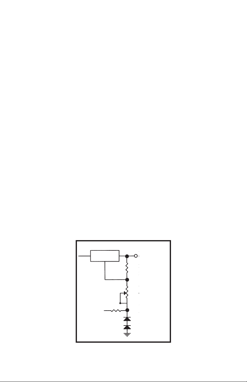
REGULATOR CIRCUIT
Figure 6
The regulator circuit in the Model XP-15 Power Supply consists of
a LM317 integrated circuit. This IC is specially designed to perform
the regulation function. Figure 6 shows a simplified circuit of how
the LM317 IC works.
1.25V
Output
R1
R2
Divider
Q1
Q2
1.5V
Q3
Q4
Q5
Current
Source
Equalized
to 1 Meg.
Page 5
-4-
Transistors Q1 and Q2 form a circuit known as a differential
amplifier. Transistor Q1’s base is connected to a stable 1.5V
reference voltage. The base of Q2 is connected to the regulator
output circuit through a voltage divider network. The collector of
transistor Q2 is connected to a current source. This basically is a
PNP transistor biased to draw about 1mA current. Transistor Q2
sees the current source as a very high resistor of about 1 meg
ohms. Thus, the gain of transistor Q2 is very high.
Transistor Q5 is called the pass transistor. It controls the current
reaching the output. Transistors Q3 and Q4 are emitter followers.
Their function is to raise the impedance of the pass transistor. Note
that transistor Q2, Q3, Q4, Q5 and resistor R1 form a closed loop.
Also, note that the feedback to the base of Q2 is negative, that is,
the output at emitter Q5 goes negative. Now, if the 1.25V output
voltage goes down because of current drain at the output, the base
of Q2 will drop, forcing the collector voltage of Q2 to go higher. This
will bring the output voltage back to 1.25V. This is the basis of all
negative feedback regulators.
Another feature of the LM317 regulator is to protect the IC against
overload and output shorts. If the IC is overloaded, the junction will
overheat. A transistor will sense this overheating and shut down
transistor Q5.
The LM317 IC is basically a 1.25V regulator. To be able to vary the
output 0 - 15V, we stack the IC on the negative 1.25VDC voltage
as shown in Figure 7. When R3 equals 0, the output voltage is 0
volts.
0V - 15V
R2
R3
LM-317
–DC
Figure 7
Page 6

SCHEMATIC DIAGRAM
REV-A
-5-
Page 7

-6-
PARTS LIST
RESISTORS
Qty. Symbol Description Part #
r 1 R2 150W 5% 1/4W 131500
r 2 R1, R4 2.2kW 5% 1/4W 142200
r 1 R3 2kW Potentiometer 192421
CAPACITORS
Qty. Symbol Description Part #
r 1 C2 4.7mF 50V Electrolytic 264747
r 1 C4 220mF 16V Electrolytic 282244
r 1 C3 470mF 35V Electrolytic 284746
r 1 C1 2,200mF 35V Electrolytic 292226
SEMICONDUCTORS
Qty. Symbol Description Part #
r 8 D1-8 1N4001 Diode 314001
r 1 U1 LM317 Regulator 330317
r 1 D9 LED Red 350002
MISCELLANEOUS
Qty. Symbol Part #
r 1 Transformer YD-1485 440111
r 1 PC board 510002
r 1 Heat sink 615009
r 1 Knob 622009
r 1 Case top 623061
r 1 Case bottom 623062
r 1 Strain relief 2-wire 624002
r 1 Binding post black 625031
r 2 Nut binding post 625031HN
r 2 Lockwasher binding post 625031LW
r 1 Binding post red 625032
r 4 Screw 3 x 8mm 641102
r 1 Screw 4-40 x 1/4” 641430
r 2 Screw 6-32 x 3/8” Blk 641652
r 1 Nut 7mm 644101
r 1 Nut 4-40 644400
r 2 Nut 6-32 644600
r 1 Washer flat 8 x 14mm 645101
r 4 Washer fiber #6 645602
r 2 Lockwasher #6 646600
r 4 Rubber foot 662015
r 1 Label top 723071
r 1 Line cord 2 wire 862100
r 2” Shrink tubing 890120
Page 8

ELENCO
®
150 Carpenter Ave.
Wheeling, IL 60090
(847) 541-3800
Website: www.elenco.com
e-mail: elenco@elenco.com
TWO YEAR WARRANTY
All Elenco®models are guaranteed for two
full years on all parts and service. For the
first 3 months, your power supply is covered
at absolutely no charge. For the remaining
21 months, a nominal service charge is
required to cover shipping and handling.
When returning merchandise for repair,
please include proof of purchase, a brief
letter of explanation of problem, and
sufficient packing material. Before
returning any merchandise please call
our service department at (847) 541-3800
to obtain a return authorization number
(RMA).
 Loading...