

Page 1
Page 2
Outline
Page # Title Page # Title
3 Parts List 17 Project 10: S-R NAND Latch
4-7 Introduction 18 Project 11: Gated S-R Latch
8 Project 1: NOT Gate (Inverter) 19-20 Project 12: J-K Latch
9 Project 2: AND Gate 21-22 Project 13: Gated D Latch
10 Project 3: OR Gate 23-24 Project 14: Comparator
11 Project 4: NAND Gate 25 Project 15: Half Adder
12 Project 5: NOR Gate 26 Project 16: Half Subtractor
13 Project 6: Exclusive OR (XOR) Gate 27-28 Project 17: Multiplexer
2
14 Project 7: De Morgan’s Law
Negation of Conjunction
15 Project 8: De Morgan’s Law
Negation of Disjunction
16 Project 9: S-R NOR Latch
29-33 Quiz
34-41 Quiz Answers
Warning: Shock Hazard – Never connect Snap Circuits® to the electrical outlets in your home in any way!
Warning: Choking Hazard – Small parts. Not for children under 3 years.
Warning: Always check your wiring before turning on a circuit. Never leave a circuit unattended while the batteries are installed. Never connect
additional batteries or other power sources to your circuits. Discard any cracked or broken parts.
Batteries:
• Use only 1.5V AA type, alkaline batteries.
• Insert batteries with correct polarity.
• Do not mix old and new batteries.
• Remove batteries when they are used up.
• Do not short circuit the battery terminals.
• Non-rechargeable batteries should not be recharged.
Rechargeable batteries should only be charged under adult
supervision, and should not be recharged while in the product.
• Do not mix alkaline, standard (carbon-zinc), or rechargeable
(nickel-cadmium) batteries.
• Do not connect batteries or battery holder in parallel.
• Never throw batteries in a fire or
attempt to open its outer casing.
• Batteries are harmful if swallowed,
so keep away from small children.
Page 3

Parts List
ID Part Name Part Number QTY
1 1-snap wire 6SC01 7
2 2-snap wire 6SC02 10
3 3-snap wire 6SC03 5
4 4-snap wire 6SC04 1
5 5-snap wire 6SC05 2
6 6-snap wire 6SC06 1
7 7-snap wire 6SC07 2
B1 Battery Holder 4.5V (3-AA) 6SCB3 1
Base Grid (11.0” x 7.7”) 6SCBG 1
D1 LED red 6SCD1 1
D2 LED green 6SCD2 1
Jumper wire black 6SCJ1 1
Jumper wire red 6SCJ2 1
Jumper wire orange 6SCJ3A 1
Jumper wire green 6SCJ3C 3
Jumper wire gray 6SCJ3E 5
R2
S1 Slide switch 6SCS1 1
U15 NOT Gate 6SCU15 3
U16 AND Gate 6SCU16 2
U17 OR Gate 6SCU17 1
U18 NAND Gate 6SCU18 2
U19 NOR Gate 6SCU19 2
U20 XOR Gate 6SCU20 1
1kΩ Resistor
6SCR2 2
3
Page 4
Introduction
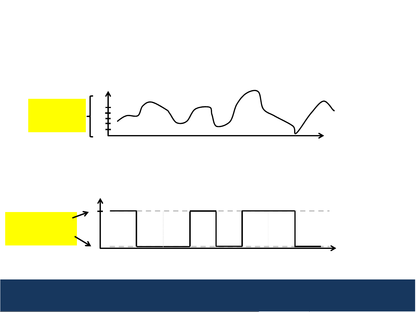
Analog signals can take on a continuum of values while
Analog vs. Digital Waveforms
Analog Waveform – can take on any voltage value
Voltage
4
Analog Signal
takes on a
Continuum of
Voltage values
5
4
3
2
1
0
Time
Digital Waveform – takes on discrete voltage values
Voltage
5
Example of Digital
Signal taking on two
discrete values
(0 Volts and 5 Volts)
0
Time
digital signals take on only discrete values.
Page 5
Introduction
Digital Signals
Digital waveforms can be used to represent digital
signals (e.g. 0 or 1, true or false), for example
• 0 (false) – represented by 0 Volts
• 1 (true) – represented by a small voltage, e.g. 3 Volts
Example of Digital Waveform representing digital
5
signals
3V
0V
Digital signals are represented by a “high” state (1) or “true” state consisting of a small voltage
(e.g. 3V) and “low” state (0) or “false” state consisting of 0 Volts.
True
1 0 0 1 0 1 1 0
False
False
True
False
True
True
False
Time
Page 6
Introduction
only if both inputs are true (batteries are not dead AND it’s the top of the hour).
Logic Problem Statements
Logic problems have outcomes (or outputs) that depend on events
(or inputs).
For example
• The cuckoo clock makes noise if the batteries are not dead AND it’s the top of
the hour.
• In this example, the output is “the cuckoo clock making noise” and the inputs
are “the batteries are not dead” and “it’s the top of the hour”.
6
Batteries not dead?
Top of the hour?
Decision
Cuckoo clock makes noise?
Box
• Note that in this example, the output is true (cuckoo clock makes noise) if and
• You will see that this decision box can be represented by digital logic using an
AND gate, with the inputs and output being represented by digital signals.
You can think of digital logic gates as decision boxes that solve logic problems.
Page 7

Introduction
Logic Gates
A digital logic gate is an Integrated Circuit (IC) device that
makes logical decisions based on various combinations of
digital signals presented to it’s inputs.
Digital logic gates can have more than one input signal,
but generally have a single output signal, just like the
decision box on the previous slide.
In the following projects, the input digital signals will be
represented by A and/or B and the output digital signal
will be represented by Q.
7
The next six projects will demonstrate how the output
Input Digital
digital signal is determined by the input digital signals for
various different digital logic gates (NOT gate, AND gate,
Signals
Output Digital
Signal
OR gate, NAND gate, NOR gate, XOR gate).
A
Digital Logic
The remaining projects will demonstrate the input/output
Gate
characteristics of some common combinations of digital
B
logic gates, called digital logic circuits.
Almost all modern electronics such as computers and cellphones use digital logic circuitry.
Q
Page 8
Project 1: NOT Gate (Inverter)
8
1
0
2
1
3
This circuit demonstrates how the NOT
Gate (U15) works. Turn the slide switch
(S1) on. Connect the loose end of the
A
2
2
U15
1
Q
1
2
1
red wire to either low voltage (denoted
as a “0”) or high voltage (denoted as
“1”). If input A is low (0), then the Q
output will be high (1), and the red LED
(D1) will be on. If input A is high (1),
then the Q output will be low (0) and
3
2
2
1
2
3
1
2
the red LED will be off.
A
Q
The inversion of a state is often
represented with a bar over the
variable, so Q = A.
Input (A) Output (Q)
0 1
1 0
NOT gates are used in digital logic circuits to “invert a voltage level”. A high voltage level (1)
into the NOT gate becomes a low voltage level (0) at the output and vice versa.
Page 9
1
0
9
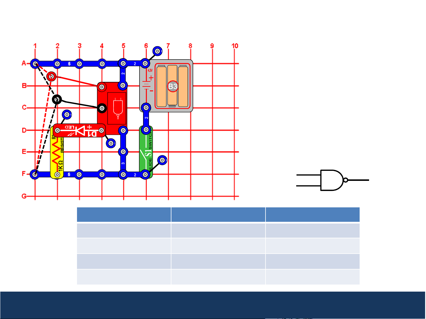
Project 2: AND Gate
This circuit demonstrates how the AND
2
1
2
3
A
2
B
1
2
1
2
3
Q
U16
1
2
2
2
1
3
1
2
Gate (U16) works. Turn the slide switch
(S1) on. Connect the loose ends of the red
and black wires to either low voltage
(denoted as a “0”) or high voltage
(denoted as a “1”). If, and only if, both
input A AND input B are high (both 1s),
then the Q output will be high (1), and the
red LED (D1) will be on.
A
Q
B
The output of an AND gate is often
represented as the product of the
inputs, so Q = AB.
Input (A) Input (B) Output (Q)
0 0 0
0 1 0
1 0 0
1 1 1
AND gates are used in digital logic circuits to perform a logical multiply. When one of the inputs is low (0),
the output is low (i.e. multiply by 0). The output will only be high (1) when both inputs are high.
Page 10
1
0
10
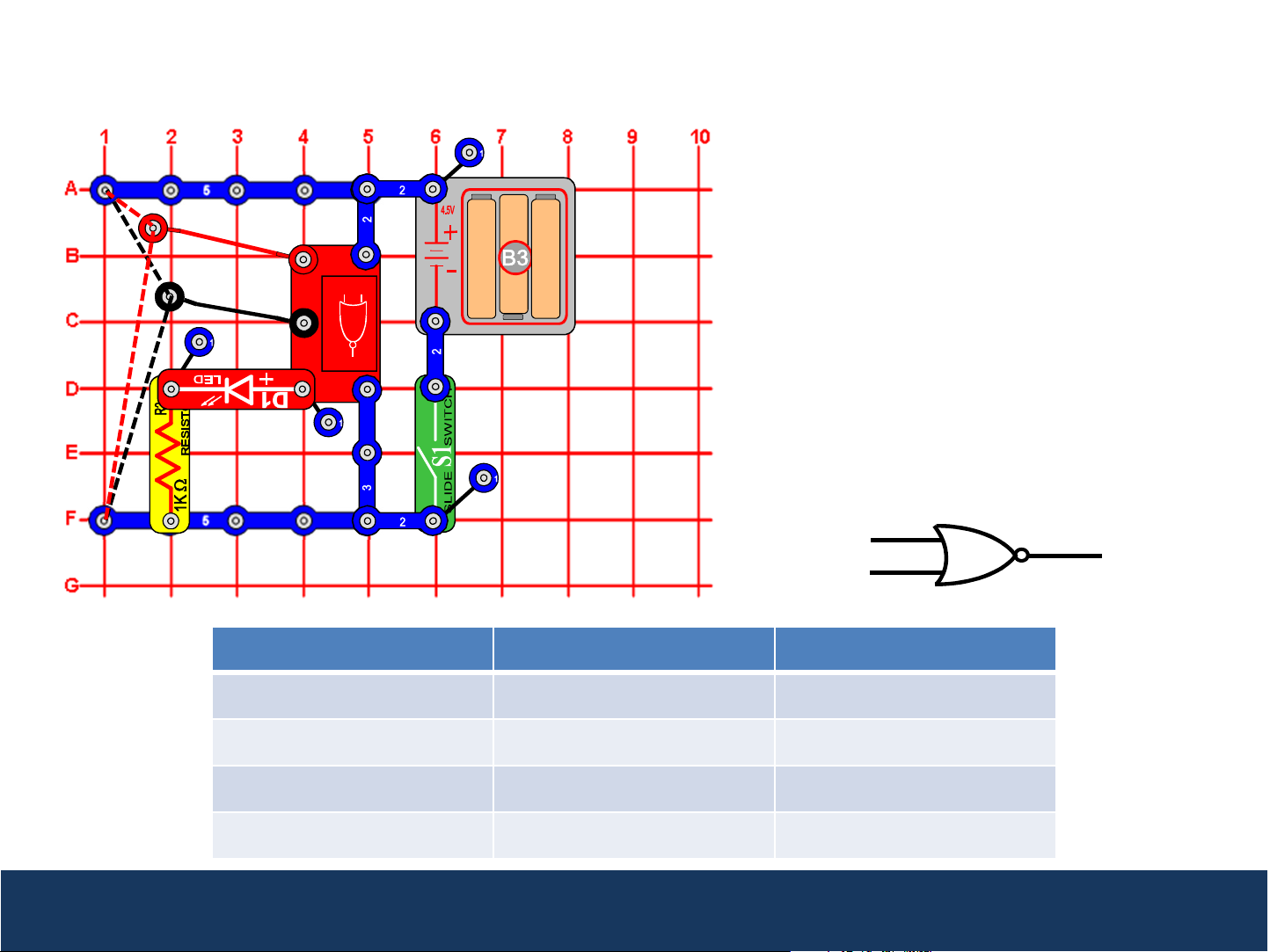
Project 3: OR Gate
2
This circuit demonstrates how the OR Gate
1
2
A
2
B
1
2
1
2
3
Q
2
2
3
(U17) works. Turn the slide switch (S1) on.
Connect the loose ends of the red and
black wires to either low voltage (denoted
as a “0”) or high voltage (denoted as a
U17
“1”). If either input A OR input B are high
1
2
1
(1), then the Q output will be high (1), and
the red LED (D1) will be on.
1
A
Q
B
2
3
The output of an OR gate is often
represented as the sum of the inputs, so
Q = A+B.
Input (A) Input (B) Output (Q)
0 0 0
0 1 1
1 0 1
1 1 1
OR gates are used in digital logic circuits to perform a logical add. When one of the inputs is high (1), the
output is high. The output will only be low (0) when both inputs are low.
Page 11
Project 4: NAND Gate
11
1
0
2
1
3
This circuit demonstrates how the NAND
Gate (U18) works. Turn the slide switch (S1)
on. Connect the loose ends of the red and
2
A
2
B
1
2
U18
1
2
1
black wires to either low voltage (denoted as
a “0”) or high voltage (denoted as a “1”). If
either input A OR input B are low (0), then
the Q output on U18 will be high (1), and the
red LED (D1) will be on. The output logic is
exactly the opposite of the AND gate, hence
3
Q
2
2
1
2
3
1
this gate is called the NOT AND or NAND
Gate.
2
A
Q
B
Input (A) Input (B) Output (Q)
0 0 1
0 1 1
1 0 1
1 1 0
NAND gates are used in digital logic circuits to perform an inverted logical multiply. When one of the
inputs is low (0), the output is high. The output will only be low (0) when both inputs are high.
Page 12
Project 5: NOR Gate
12
1
0
2
1
2
3
A
2
B
1
2
U19
1
2
1
This circuit demonstrates how the NOR Gate
(U19) works. Turn the slide switch (S1) on.
Connect the loose ends of the red and black
wires to either low voltage (denoted as a
“0”) or high voltage (denoted as a “1”). If,
and only if, both input A AND input B are
low (0), then the Q output on U19 will be
high (1), and the red LED (D1) will be on.
3
Q
2
2
1
2
3
1
2
The output logic is exactly the opposite of
the OR gate, hence this gate is called the
NOT OR or NOR Gate.
A
Q
B
Input (A) Input (B) Output (Q)
0 0 1
0 1 0
1 0 0
1 1 0
NOR gates are used in digital logic circuits to perform an inverted logical add. When one of the inputs is
high (1), the output is low. The output will only be high (1) when both inputs are low.
Page 13
Project 6: Exclusive OR (XOR) Gate
2
13
1
0
1
2
A
2
B
1
2
3
This circuit demonstrates how the Exclusive
OR (XOR) Gate (U20) works. Turn the slide
switch (S1) on. Connect the loose ends of
the red and black wires to either low voltage
U20
1
2
1
(denoted as a “0”) or high voltage (denoted
as a “1”). If input A and input B are
exclusive (i.e. different), then the Q output
3
Q
2
2
1
2
3
1
2
on U20 will be high (1), and the red LED (D1)
will be on.
A
Q
B
Input (A) Input (B) Output (Q)
0 0 0
0 1 1
1 0 1
1 1 0
XOR gates are used in digital logic circuits to perform a comparison. When the inputs are mutually exclusive
(i.e. different), then the output is high (1). When the inputs are the same, then the output is low (0).
Page 14
14
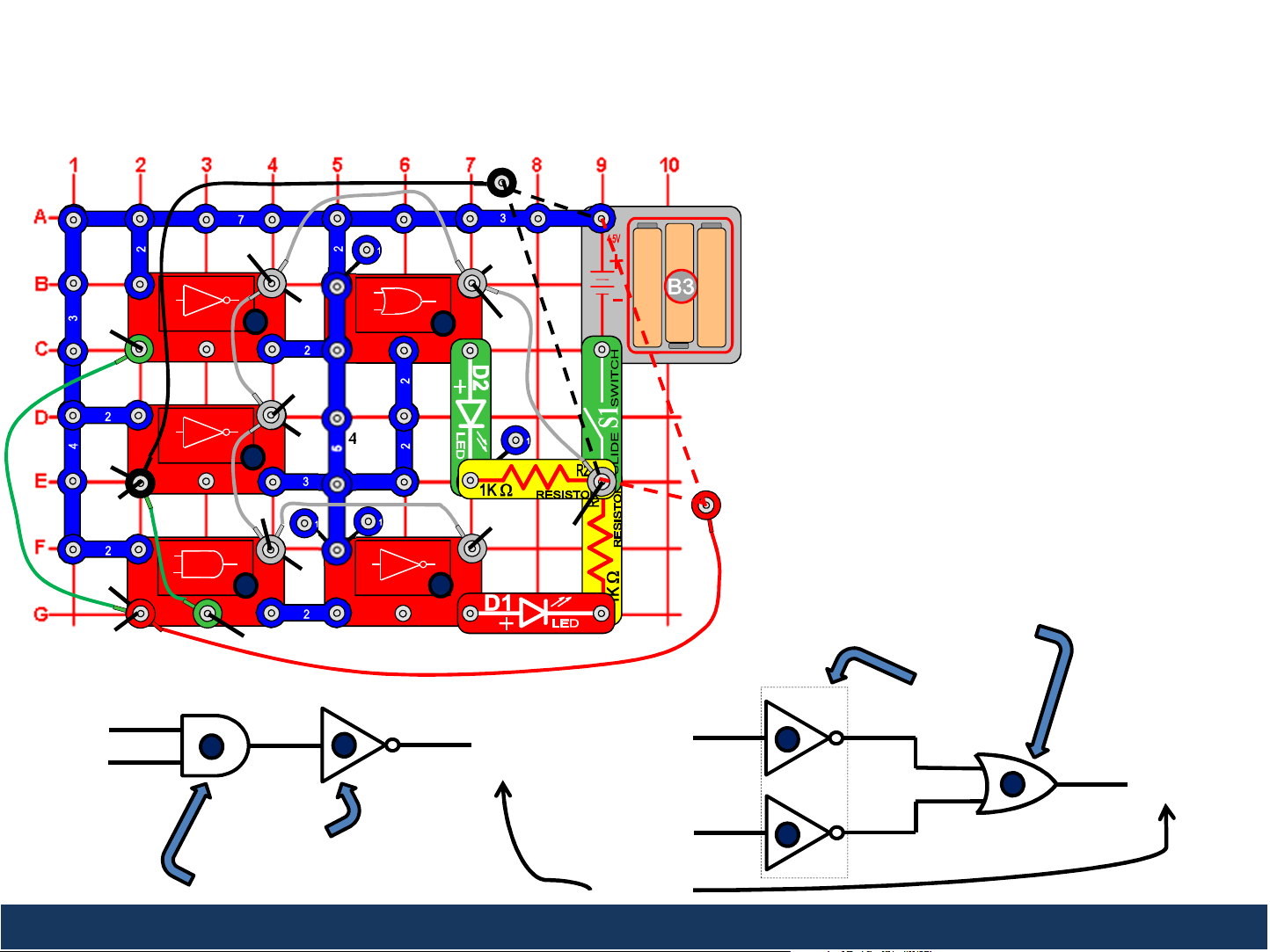
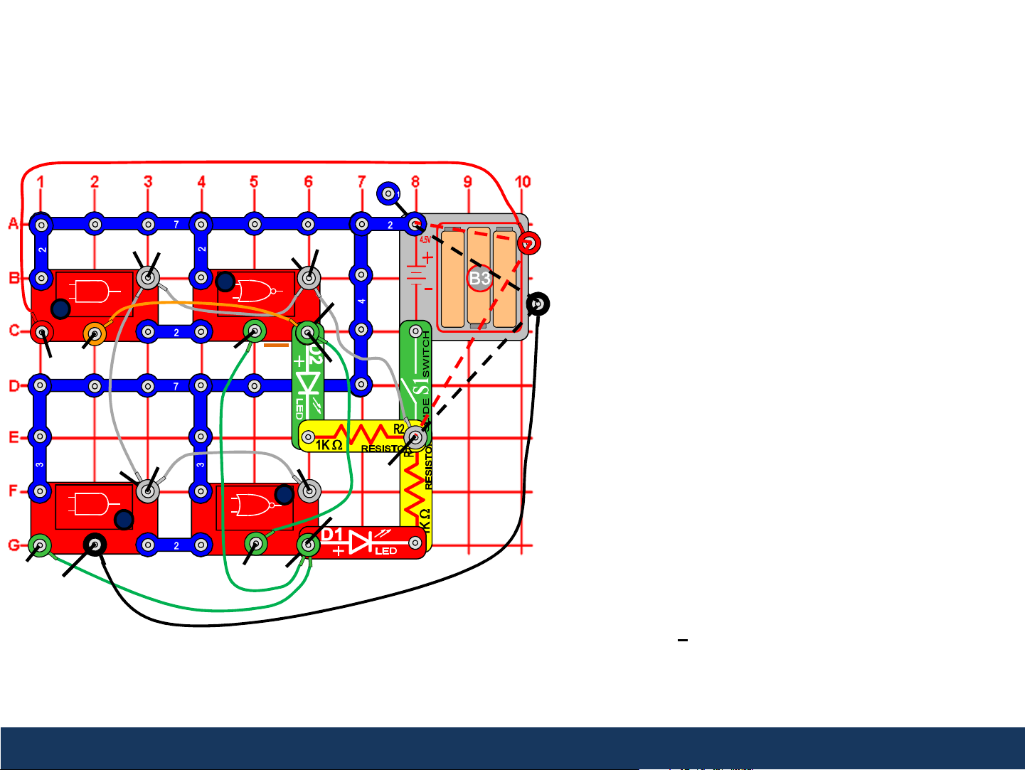
Project 7: De Morgan’s Law
Negation of Conjunction
This circuit demonstrates De Morgan’s Law of
1
2
2
2
2
1
2
3
2
2
U15
U15
B
U16
3
1
3
1
4
3
1
1
2
2
2
3
2
2
3
2
2
3
1
U17
5
2
4
2
U15
1
1
2
2
2
Q
2
2
3
1
3
2
1
1
2
4
0
1
Negation of Conjunction which states that the
negation of a conjunction is equivalent to
disjunction of the negations. Turn the slide switch
(S1) on. The green wire on the left connects the A
inputs of the top U15 module and the U16 module
(representing the A input in the diagrams below)
while the green wire on the right connects the B
inputs of the second U15 module and the U16
module (representing the B input in the diagrams
below). Connect the loose ends of the red wire and
the black wire to either high voltage (1) or low
voltage (0). No matter what combination you
connect, the green LED and red LED will always
either both be on or both be off, demonstrating that
any combination of inputs to the two diagrams
always provides the same outputs.
A
B
3
A
2
Q
Disjunction
of
Negations
1
Negation
2
Q
A
=
B
3
5
4
Q
of
Conjunction
Same
Negation of Conjunction = Disjunction of Negations.
Page 15

15
Project 8: De Morgan’s Law
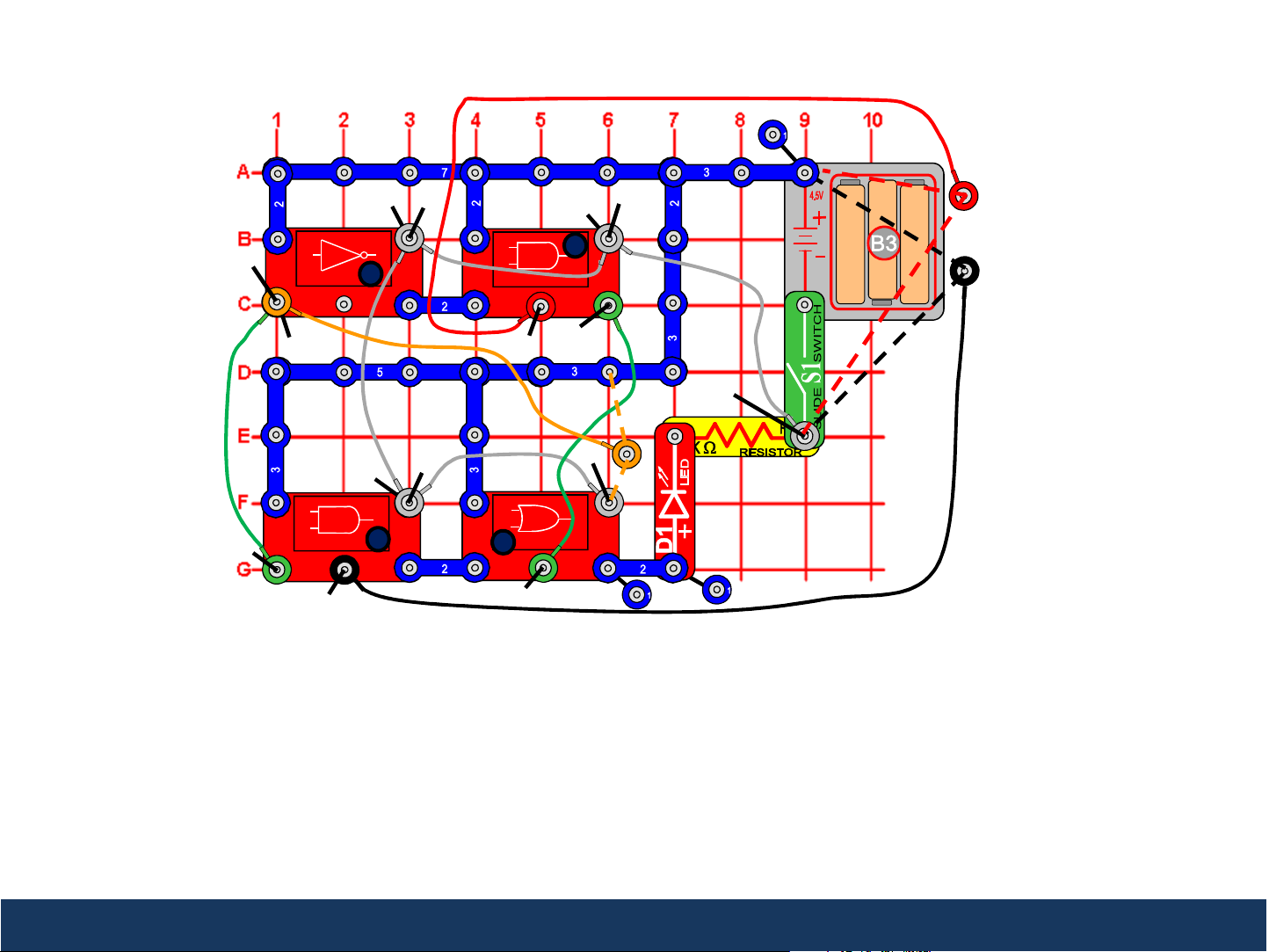
Negation of Disjunction
This circuit demonstrates De Morgan’s Law of
3
1
2
2
2
2
1
2
3
2
2
U15
U15
B
3
1
3
1
4
3
1
U17
1
2
2
2
3
2
2
3
2
2
3
1
U16
5
2
4
2
U15
1
1
2
2
Q
2
2
2
3
1
3
2
1
1
2
4
0
1
Negation of Disjunction which states that the
negation of a disjunction is equivalent to
conjunction of the negations. Turn the slide switch
(S1) on. The green wire on the left connects the A
inputs of the top U15 module and the U17 module
(representing the A input in the diagrams below)
while the green wire on the right connects the A
inputs of the second U15 module and the U17
module (representing the B input in the diagrams
below). Connect the loose ends of the red wire and
the black wire to either high voltage (1) or low
voltage (0). No matter what combination you
connect, the green LED and red LED will always
either both be on or both be off, demonstrating that
any combination of inputs to the two diagrams
always provides the same outputs.
A
B
3
A
2
Q
Conjunction
of
Negations
1
Negation
2
Q
A
=
B
3
5
4
Q
of
Disjunction
Same
Negation of Disjunction = Conjunction of Negations.
Page 16

S
16
Project 9: S-R NOR Latch
This circuit demonstrates how the S-R NOR Latch works.
Turn the slide switch (S1) on. Connect the loose end of
the red wire (S input) to 0 and the loose end of the black
wire (R input) to 1. The red LED will be off (S=0, R=1
1
1
2
U19
2
2
4
0
3
1
1
2
2
Q
1
2
1
2
2
1
U19
2
2
2
1
Q
2
2
2
3
2
1
3
R
1
resets output Q to 0). Now disconnect the black wire
from 1 and connect it to 0. The red LED remains off (S=0,
R=0 holds the last output state). Now disconnect the red
wire from 0 and connect it to 1. The red LED will be on
(S=1, R=0 sets the output to 1). Now disconnect the red
wire from 1 and connect it to 0. The red LED remains on
(S=0, R=0 holds the last output state). S=R=1 is the
forbidden state, can you explain why? The green LED
should always be the opposite of the red LED (green LED
off when red LED on and green LED on when red LED off)
since the green LED represents Q which is the opposite
of Q.
R
1
Q
Input (S) Input (R) Output (Q) Output (Q)
0 0 Hold State Hold State
1 0 1 0
0 1 0 1
1 1 Not Allowed Not Allowed
S-R NOR Latches can be used to eliminate bouncing in switches.
2
Q
S
Stays the same when S=R=0
Reset to 0 when S=0 & R=1
Set to 1 when S=1 & R=0
S=R=1 is forbidden
Page 17

S
Project 10: S-R NAND Latch
This circuit demonstrates how the S-R NAND Latch
works. Turn the slide switch (S1) on. Connect the loose
end of the red wire (S input) to 1 and the loose end of
1
1
2
U18
2
4
2
0
3
2
1
2
Q
2
1
1
2
2
1
U18
2
2
1
1
2
Q
2
2
2
3
1
3
1
R
the black wire (R input) to 0. The red LED will be off
(S=1, R=0 resets output Q to 0). Now disconnect the
black wire from 0 and connect it to 1. The red LED
remains off (S=1, R=1 holds the last output state). Now
disconnect the red wire from 1 and connect it to 0. The
red LED will be on (S=0, R=1 sets the output to 1). Now
disconnect the red wire from 0 and connect it to 1. The
red LED remains on (S=1, R=1 holds the last output
state). S=R=0 is the forbidden state, can you explain
2
why? The green LED should always be the opposite of
the red LED (green LED off when red LED on and green
LED on when red LED off) since the green LED represents
Q which is the opposite of Q.
S
17
1
Q
Input (S) Input (R) Output (Q) Output (Q)
0 0 Not Allowed Not Allowed
1 0 0 1
0 1 1 0
1 1 Hold State Hold State
S-R NAND Latch is an alternative to S-R NOR Latch where the inputs S and R are now active low.
2
R
Q
Stays the same when S=R=1
Reset to 0 when R=0 & S=1
Set to 1 when R=1 & S=0
S=R=0 is forbidden
Page 18

Project 11: Gated S-R Latch
18
2
S
2
1
3
2
U16
2
1
2
2
2
E
1
U19
1
3
2
3
0
2
1
3
1
This circuit demonstrates how a Gated S-R Latch
works. Turn the slide switch (S1) on. Connect one
the loose end of the orange wire to 1 (Latch
enabled). Repeat the experiments from Project 9
to verify that this now functions as an S-R NOR
Latch. Now with S=1 and R=0 (red LED should be
on), disconnect the orange wire from 1 and
3
3
2
1
2
3
2
Q
2
1
connect it to 0 (Latch disabled). The red LED
should now remain on no matter whether you
connect the red and black wires to 1 or 0. Now
with S=0 and R= 1, move the orange wire back to 1
2
2
1
U16
3
2
1
2
1
U19
2
4
Q
3
4
2
0
1
(Latch enabled so red LED should go off). Now
move the orange wire back to 0 again (Latch
disabled). The red LED should now remain off no
matter whether you connect the red and black
wires to 1 or 0. The green LED should always be the
2
2
R
2
3
opposite of the red LED (green LED off when red
LED on and green LED on when red LED off) since
the green LED represents Q which is the opposite
of Q.
Input (E) Q, Q
0 Hold State
1 Same as S-R Latch
The Enable input (E) can be used as a clock input, or a read/write strobe.
Operates as S-R
Latch when E=1
Holds output
state when E=0
R
S
E
1
2
4
3
Q
Q
Page 19
2
J
19
Project 12: J-K Latch
This circuit demonstrates how a J-K Latch works. Turn
the slide switch (S1) on. Connect the loose ends of
2
1
2
2
1
U16
1
2
2
2
1
2
U16
K
2
3
2
2
1
4
U19
2
Q
1
3
2
2
2
1
U19
2
3
2
3
2
4
2
2
3
3
4
2
3
Q
1
3
1
2
0
4
1
the red and black jumper wires to either 0 or 1.
When the red jumper is connected to 0 & the black
jumper is connected to 1, then the red LED will be
off (J=0, K=1 resets the output to 0)
When the red jumper is connected to 1 & the black
jumper is connected to 0, then red LED will be on
(J=1, K=0 sets the output to 1)
When the red & black jumpers are both connected
to 0, then the red LED will stay the same
• Try starting with the LED off (J=0, K=1) and then move the
black lead to 0 (K=0) to see that the red LED stays off
• Try starting with the LED on (J=1, K=0) and then move the
red lead to 0 (J=0) to see that the red LED stays on
When the red & black jumpers are both connected
to 1, then the red LED will toggle between on & off
continuously (J=1, K=1 toggles output)
• Note that the red and green LEDs appear dim when J=K=1
since they are toggling between on and off
The green LED should always be the opposite of the
red LED (green LED off when red LED on and green
LED on when red LED off) since the green LED
represents Q which is the opposite of Q.
Details of the J-K Latch Block Diagram and Logic Chart on Next Page.
Page 20

K
20
Project 12: J-K Latch
Stays the same when J=K=0
1
4
Q
Reset to 0 when J=0 & K=1
Set to 1 when J=1 & K=0
Toggles when J=K=1
J
2
Input (J) Input (K) Output (Q) Output (Q)
0 0 Hold State Hold State
1 0 1 0
0 1 0 1
1 1 Toggle Toggle
J-K Latches and flip flops are used for memory devices and counters.
3
Q
Page 21

Project 13: Gated D Latch
21
3
2
U16
4
2
2
E
2
2
1
U16
2
1
1
3
5
U15
1
2
2
3
D
3
2
2
1
4
1
2
Q
3
3
3
2
2
2
3
2
2
4
2
3
2
2
1
U19
2
3
U19
3
1
2
1
3
2
0
2
1
2
2
2
4
3
1
2
1
Q
This circuit demonstrates how a Gated D Latch works. Turn the slide switch (S1) on. Connect one end of the red
jumper wire to the A input of the lower U16 module and the B input of the upper U16 module (this represents the E
input) and connect the loose end of the red wire to 1 (Latch enabled). Connect one end of the black wire to the A
input of the U15 on the left and the B input of the lower U16 module (this represents the D, or data, input). Note that
when you connect the loose end of the black wire to 1, the red LED is on, and when you connect the loose end of the
black wire to 0, the red LED is off. With the black wire connected to 1 (red LED on), connect the red wire to 0. Note
that the red LED remains on now, regardless of whether the black wire is connected to 1 or 0. The green LED should
always be the opposite of the red LED (green LED off when red LED on and green LED on when red LED off) since the
green LED represents Q which is the opposite of Q.
Details of the Gated D Latch Block Diagram and Logic Chart on Next Page.
Page 22

Project 13: Gated D Latch
22
D
5
1
4
Q
Stays the same when E=0
Reset to 0 when D=0 & E=1
Set to 1 when D=1 & E=1
E
2
3
Q
E D Output (Q) Output (Q)
0 0 or 1 Hold State Hold State
1 0 0 1
1 1 1 0
The Gated D Latch exploits the fact that the active input combinations on an S-R Latch
(S=1, R=0 and S=0, R=1) produce opposite outputs. Thus, the Gated D Latch can be thought of
as a single input Gated S-R Latch. Gated D Latches can be used as Input/Output (I/O) ports.
Page 23

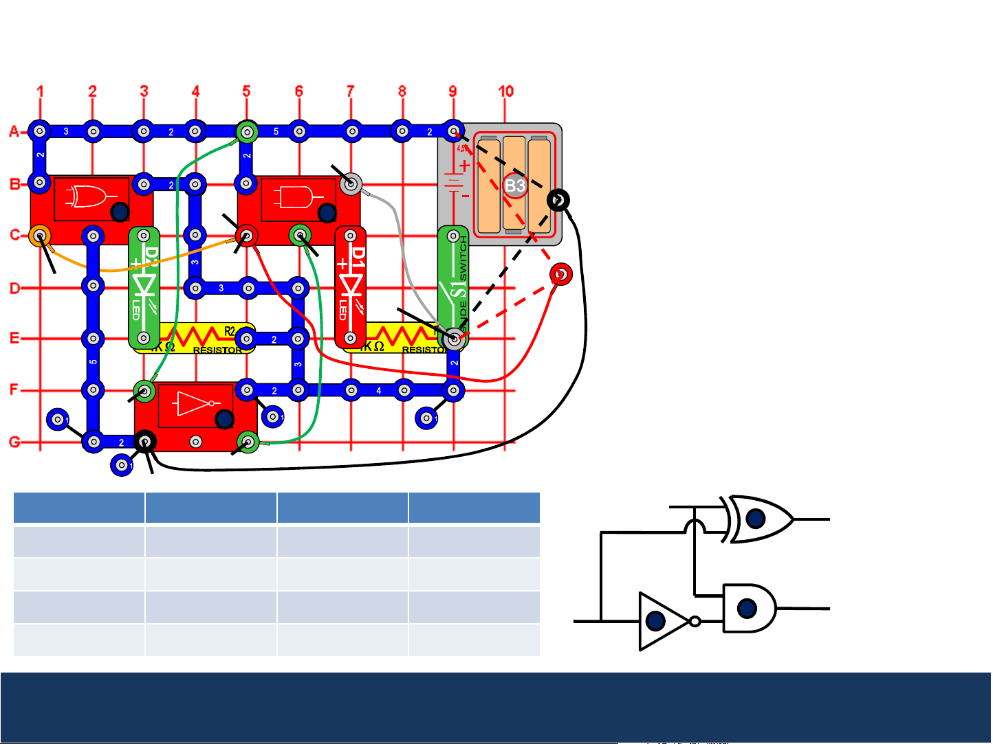
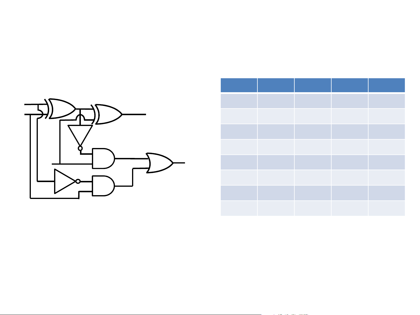
Project 14: Comparator
2
23
2
3
A
1
2
2
2
2
1
1
U15
2
U15
2
3
B
3
2
1
2
1
3
2
2
1
U16
2
1
U16
3
2
4
2
3
2
2
3
3
2
2
3
2
0
1
U19
1
1
2
1
2
3
2
1
5
2
Q
1
2
This circuit demonstrates how a comparator works. Turn the slide switch (S1) on. When the loose ends
of the red and black wires are connected to the same input (either 1 or 0), the red LED will be on
(indicating the inputs are the same). When the loose ends of the red and black wires are connected to
different inputs (one to 1 and the other to 0), the red LED is off (indicating the inputs are different).
Can you think of a much simpler circuit than the one above that achieves the same result (hint: it can
be done with just 2 gates)?
Details of the Comparator Block Diagram and Logic Chart on Next Page.
Page 24

Project 14: Comparator
Comparators are used in Central Processing Units (CPUs) and
24
A
B
1
4
Equal to 1 when A=B
Equals 0 when A ≠ B
5
3
2
Q
Simpler Comparator Circuit
A
Q
B
A B Output (Q)
0 0 1
0 1 0
1 0 0
1 1 1
Page 25

Project 15: Half Adder
in computers and processors as arithmetic logic units,
25
1
2
U20
1
2
2
2
S
1
2
1
U16
2
2
2
1
1
B
1
2
2
2
3
1
2
1
A
2
3
2
3
2
1
Input (A) Input (B) Output (S) Output (C)
0 0 0 0
C
2
4
1
3
2
0
1
This circuit demonstrates how a half adder
works. Turn the slide switch (S1) on. The
green LED represents the Sum (S) and the red
LED represents the Carry (C). When the loose
ends of the red and black wires are both
connected to 0 (0+0), both LEDs are off
(S=C=0). When one of the loose ends of the
red and black wires are connected to different
inputs (one to 0 and the other to 1), the green
LED is on and the red LED is off (S=1, C=0).
When the loose ends of the red and black
wires are both connected to 1 (1+1), the green
LED is off and the red LED is on (S=0, C=1)
indicating an overflow condition.
A
1
Represents the
S
Sum
0 1 1 0
1 0 1 0
1 1 0 1
2
B
Represents the
C
Carry
Adders are used
as well as to calculate addresses, table indices, etc..
Page 26
Project 16: Half Subtractor
26
2
1
2
1
1
This circuit demonstrates how a half
subtractor works. Turn the slide switch (S1)
2
2
U20
1
2
2
1
U16
2
3
1
B
1
2
2
3
1
2
1
2
2
2
2
4
on. The green LED represents the Difference
(D) of input A minus input B and the red LED
represents the Borrow (B). When the loose
ends of the red and black wires are both
connected to 0 (0-0) or to 1 (1-1), both LEDs
are off (D=B=0). When the loose end of the
red wire is connected to 1 and the loose end
of the black wire is connected to 0 (1-0), the
green LED is on and the red LED is off (D=1,
2
1
2
3
1
U15
2
1
3
2
2
1
0
3
1
A
2
4
2
B=0). When the loose end of the red is
connected to 0 and the loose end of the black
wire is connected to 1 (0-1), the green and red
LEDs are both on (D=1, B=1), indicating a
borrow condition.
Input (A) Input (B) Output (D) Output (B)
B
1
Represents the
D
0 0 0 0
0 1 1 1
1 0 1 0
A
2
3
Represents the
B
1 1 0 0
Subtractors are often implemented with adders since the incremental cost is low (one
additional NOT gate).
Difference
Borrow
Page 27
Project 17: Multiplexer
2
27
1
2
2
3
1
U15
1
2
2
1
2
2
U16
2
3
3
2
2
1
3
2
1
U16
2
1
U17
3
2
2
3
2
2
4
2
2
2
1
3
2
3
3
2
1
1
A
1
B
2
1
0
This circuit demonstrates how a multiplexer works. Turn the slide switch (S1) on. The loose end of the orange wire
represents the Selector (S). First connect the loose end of the orange wire to 1 (this selects the black input). The red
LED will now be on when the black wire is connected to 1 and off when the black wire is connected to 0 (regardless of
what the red wire is connected to). Now connect the loose end of the orange wire to 0 (this selects the red input).
The red LED will now be on when the red wire is connected to 1 and off when the red wire is connected to 0
(regardless of what the black wire is connected to).
Details of the Multiplexer Block Diagram and Logic Chart on Next Page.
Page 28

Project 17: Multiplexer
S represents the Selector
28
A
B
4
S
Equals A when S=1
Equals B when S=0
1
2
3
Q
Input (A) Input (B) Input (S) Output (Q)
0 or 1 0 0 0
0 or 1 1 0 1
0 0 or 1 1 0
1 0 or 1 1 1
Multiplexers are often used as switches (e.g. telephone line switch, HDMI switch, etc.).
Page 29

Quiz
1. The output will be LOW (0) for any case when one or more input is LOW (0) for a(n):
a) OR gate
b) NAND gate
c) AND gate
d) XOR gate
2. The output of a NOR gate is HIGH (1) if:
a) All inputs are HIGH (1)
b) Any input is HIGH (1)
c) Any Input is LOW (0)
d) All inputs are LOW (0)
29
3. Which of the following is true about a 2-input NAND gate:
a) If one of the inputs is HIGH (1), then the output is always the same as the opposite of the other input
b) There are 8 possible input combinations
c) The output is LOW (1) if any input is HIGH (1)
d) If one of the inputs is LOW (0), then the output is always the same as the other input
Page 30

30
Quiz
4. Explain why S=R=1 is not allowed for the S-R NOR circuit.
5. Using De Morgan’s laws, show how you can derive the S-R NAND gate circuit from the S-R
NOR circuit. Note that the outputs of an S-R NOR latch are the opposite of the S-R NAND
latch.
6. Draw the truth table for the circuit below?
A
B
Q
Q
Input
(A)
0 0
1 0
0 1
1 1
Input
(B)
Output
(Q)
Output
(Q)
Page 31

Quiz
7. What latch is the circuit in question 8 equivalent to?
a) D Latch
b) S-R NOR Latch
c) S-R NAND Latch
d) J-K Latch
8. Show how you would create a gated S-R NAND latch.
9. Which of the following is NOT true about a J-K latch:
a) It has a “not allowed” state
31
b) J-K latches are sometimes used in counters
c) J-K latches are sometimes used in memory devices
d) The J-K latch is an extension of the S-R NOR latch that eliminates the “not allowed” state
Page 32

Quiz
10. Show how a comparator can be built with only 2 gates.
11. The figure below represents a full adder circuit. A & B are the inputs and Ci is the carry
input, while S is the output and Co is the carry output. Complete the truth table for the
outputs of this full adder circuit.
A B Ci S Co
0 0 0
32
A
B
Ci
0 0 1
S
0 1 0
0 1 1
1 0 0
Co
1 0 1
1 1 0
1 1 1
Page 33
Quiz
12. The figure below represents a full subtractor circuit. A & B are the inputs and Bi is the
borrow input, while S is the output and Co is the borrow output. Complete the truth
table for the outputs of this full adder circuit.
A B Bi S Bo
33
A
B
S
Bi
13. Design a 4-input multiplexer circuit.
Bo
0 0 0
0 0 1
0 1 0
0 1 1
1 0 0
1 0 1
1 1 0
1 1 1
Page 34

Quiz Answers
1. The output will be LOW (0) for any case when one or more input is LOW (0) for a(n):
a) OR gate
b) NAND gate
c) AND gate
d) XOR gate
2. The output of a NOR gate is HIGH (1) if:
a) All inputs are HIGH (1)
b) Any input is HIGH (1)
c) Any Input is LOW (0)
d) All inputs are LOW (0)
34
3. Which of the following is true about a 2-input NAND gate:
a) If one of the inputs is HIGH (1), then the output is always the opposite of the other input
b) There are 8 possible input combinations
c) The output is LOW (1) if any input is HIGH (1)
d) If one of the inputs is LOW (0), then the output is always the same as the other input
Page 35

Quiz Answers
4. Explain why S=R=1 is not allowed for the S-R NOR Latch circuit.
When S=R=1, this forces both the Q and Q outputs to always be low (0), thus violating the
logical equation that Q = not Q
35
Page 36

Quiz Answers
5. Using De Morgan’s laws, show how you can derive the S-R NAND gate circuit from the
S-R NOR circuit. Note that the outputs of an S-R NOR latch are the opposite of the S-R
NAND latch.
36
S-R NOR
R
S
=
R
S
Q
Q
=
R
S
Q
Q
=
R
S
R
Q
=
Q
S
S-R NAND
Q
Q
Q
Q
This shows that
outputs of S-R
NAND latch are
the opposite of
the S-R NOR
latch
Page 37

Quiz Answers
6. Draw the truth table for the circuit below?
37
A
B
Q
Q
7. What latch is the circuit in question 8 equivalent to?
a) D Latch
b) S-R NOR Latch
c) S-R NAND Latch
d) J-K Latch
Input
(A)
0 0 Hold Hold
1 0 1 0
0 1 0 1
1 1
Input
(B)
Output
(Q)
Not
Allowed
Output
Allowed
(Q)
Not
Page 38

Quiz Answers
8. Show how you would create a gated S-R NAND latch.
38
R
E
S
9. Which of the following is NOT true about a J-K latch:
a) It has a “not allowed” state
b) J-K latches are sometimes used in counters
c) J-K latches are sometimes used in memory devices
d) The J-K latch is an extension of the S-R NOR latch that eliminates the “not allowed” state
10. Show how a comparator can be built with only 2 gates.
A
B
Q
Q
Q
Page 39

Quiz Answers
11. The figure below represents a full adder circuit. A & B are the inputs and Ci is
the carry input, while S is the output and Co is out carry output. Complete the
truth table for the outputs of this full adder circuit.
39
A
B
Ci
S
Co
A B Ci S Co
0 0 0 0 0
0 0 1 1 0
0 1 0 1 0
0 1 1 0 1
1 0 0 1 0
1 0 1 0 1
1 1 0 0 1
1 1 1 1 1
Page 40

Quiz Answers
12. The figure below represents a full subtractor circuit. A & B are the inputs and Bi is the
borrow input, while S is the output and Co is the borrow output. Complete the truth
table for the outputs of this full adder circuit.
A B Bi S Bo
40
A
B
Bi
S
Bo
0 0 0 0 0
0 0 1 1 1
0 1 0 1 1
0 1 1 0 1
1 0 0 1 0
1 0 1 0 0
1 1 0 0 0
1 1 1 1 1
Page 41

Quiz Answers
13. Design a 4-input multiplexer circuit.
41
S1
S0
A
B
Q
C
D
When S0=S1 = 0, then Q=A
When S0=1, S1=0, then Q=B
When S0=0, S1=1, then Q=C
When S0=S1=1, then Q=D
Page 42

®
ELENCO
150 Carpenter Avenue
Wheeling, IL 60090
(847) 541-3800
42
Website: www.elenco.com
e-mail: elenco@elenco.com
 Loading...