

Page 1
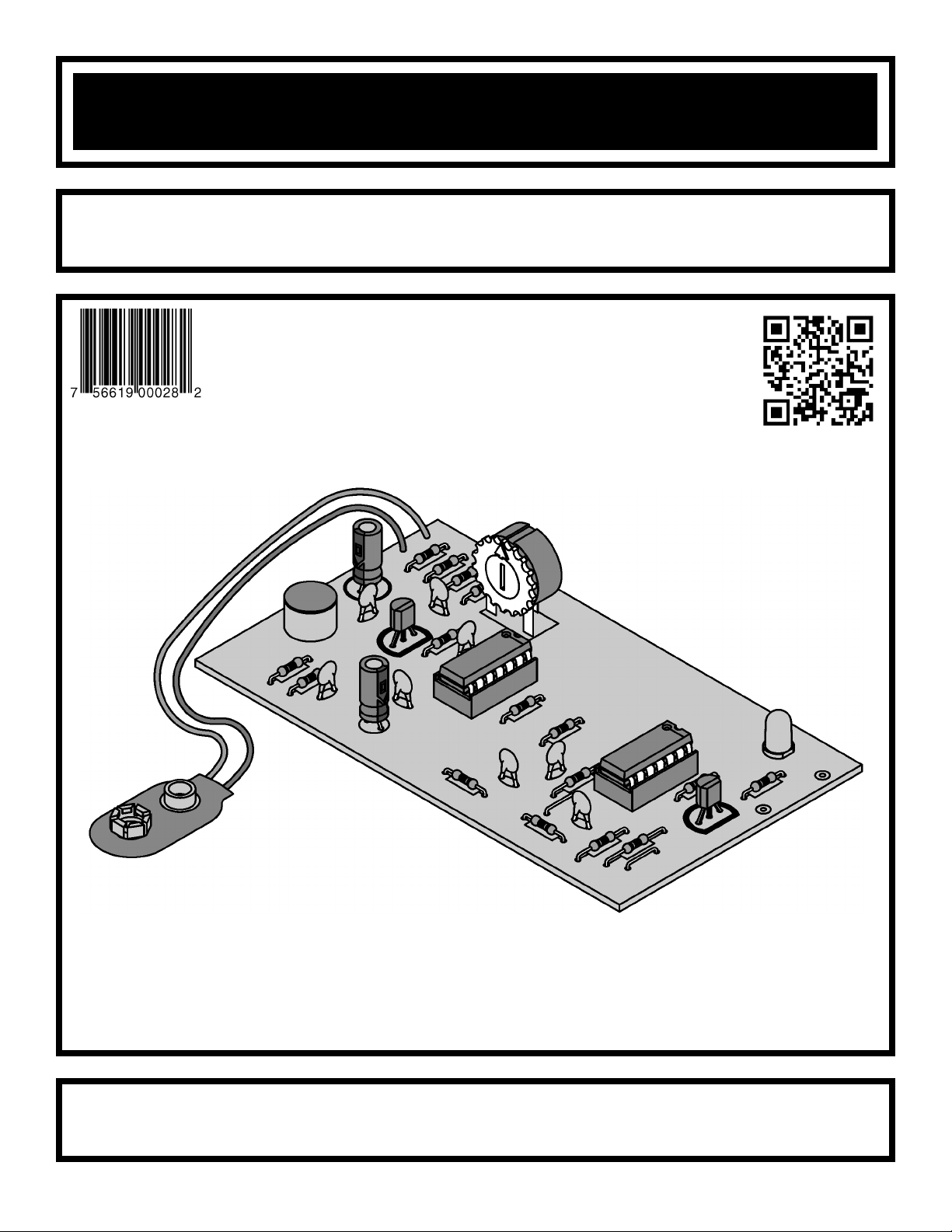
SOUND ACTIVATED SWITCH KIT
MODEL K-36
Assembly and Instruction Manual
ELENCO
®
Copyright © 2012, 1989 by Elenco®Electronics, Inc. All rights reserved. Revised 2012 REV-L 753236
No part of this book shall be reproduced by any means; electronic, photocopying, or otherwise without written permission from the publisher.
Page 2
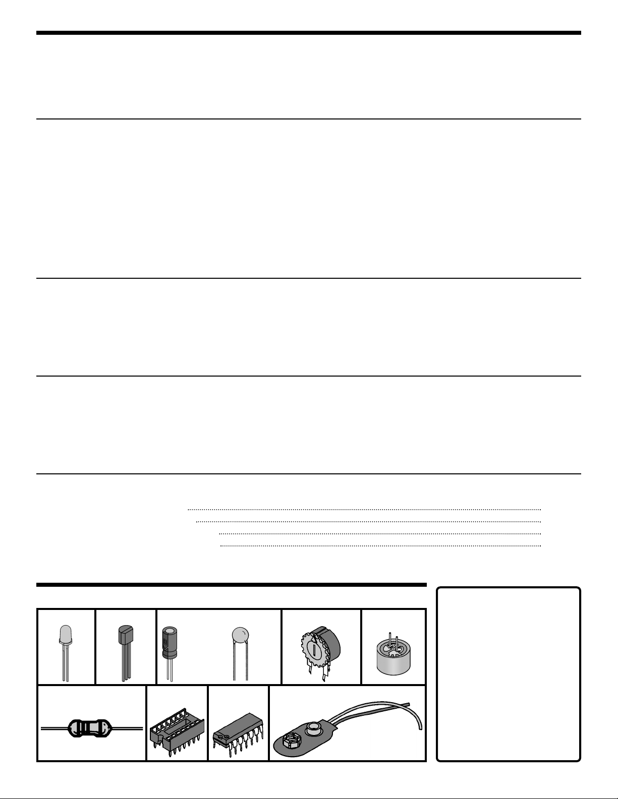
PARTS LIST
If you are a student, and any parts are missing or damaged, please see instructor or bookstore.
If you purchased this kit from a distributor, catalog, etc., please contact Elenco®(address/phone/e-mail is at the
back of this manual) for additional assistance, if needed. DO NOT contact your place of purchase as they will
not be able to help you.
RESISTORS
Qty. Symbol Value Color Code Part #
r 1 R17 4.7kΩ 5% 1/4W yellow-violet-red-gold 144700
r 3 R1, R5, R16 10kΩ 5% 1/4W brown-black-orange-gold 151000
r 1 R3 22kΩ 5% 1/4W red-red-orange-gold 152200
r 4 R4, R10, R12, R14 100kΩ 5% 1/4W brown-black-yellow-gold 161000
r 4 R2, R6, R9, R13 220kΩ 5% 1/4W red-red-yellow-gold 162200
r 1 R7 270kΩ 5% 1/4W red-violet-yellow-gold 162700
r 1 R15 330kΩ 5% 1/4W orange-orange-yellow-gold 163300
r 1 R11 1MΩ 5% 1/4W brown-black-green-gold 171000
r 1R8 4.7MΩ 5% 1/4W yellow-violet-green-gold 174700
r 1 P1 100kΩ Trim Pot 191611
CAPACITORS
Qty. Symbol Value Description Part #
r 4 C5, C6, C8, C9 .001μF (102) Discap 231036
r 2 C1, C3 .01μF (103) Discap 241031
r 2 C2, C4 .1μF (104) Discap 251010
r 1C7 1μF Electrolytic (Lytic) 261047
r 1 C10 100μF Electrolytic (Lytic) 281044
SEMICONDUCTORS
Qty. Symbol Value Description Part #
r 1 Q1 2N3904 Transistor 323904
r 1 Q2 MPS6531 Transistor 326531
r 1 U2 4001 Integrated Circuit 334001
r 1 U1 4011 Integrated Circuit 334011
r 1 LED LED Red 350002
MISCELLANEOUS
Qty. Symbol Description Part #
r 1 PC Board 518036
r 1 MIC Microphone 568000
r 1 Battery Snap 9V 590098
r 2 IC Socket 14-pin 664014
Resistor
Transistor
Potentiometer
-1-
PARTS IDENTIFICATION
LED
Capacitors
Battery SnapIC Socket Integrated
Circuit
Microphone
Electrolytic Discap
• Do not short circuit the battery terminals.
• Never throw batteries in a fire or attempt to
open its outer casing.
•
Use only 9V type alkaline battery (not
included).
• Insert battery with correct polarity.
• Do not mix alkaline, standard (carbon-zinc),
or rechargeable (nickel-cadmium) batteries.
• Non-rechargeable batteries should not be
recharged. Rechargeable batteries should
only be charged under adult supervision,
and should not be recharged while in the
product.
• Remove battery when it is used up.
• Batteries are harmful if swallowed, so keep
away from small children.
Batteries:
Page 3
-2-
INTRODUCTION
Just clap your hands together twice and watch the Sound Activated Switch turn on the light emitting diode
(LED). Clap twice more and watch the LED turn off.
THEORY OF OPERATION
Figure 1 shows the block diagram of the Sound Activated Switch. It consists of a transistor amplifier, a transistor
switch and two types of digital circuits, a one-shot and a flip-flop.
TRANSISTOR
AMPLIFIER
TRANSISTOR
SWITCH
ONE-SHOT FLIP-FLOP
Figure 1
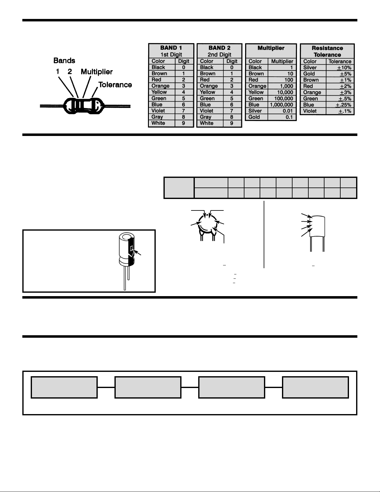
IDENTIFYING RESISTOR VALUES
Use the following information as a guide in properly identifying the value of resistors.
A waveform is created when hands are clapped
together. The MIC senses this waveform and
couples it to the base of Q1 by capacitor C1 (refer
to schematic diagram). The transistor is configured
as a common emitter amplifier since the AC signal
is bypassed to ground by capacitor C2. The
transistor amplifier is set for a gain of 50, so the
waveform is amplified 50 times. Capacitor C3
couples the amplified waveform to the input of the
first digital circuit.
THE TRANSISTOR AMPLIFIER
IDENTIFYING CAPACITOR VALUES
Capacitors will be identified by their capacitance value in pF (picofarads), nF (nanofarads), or μF (microfarads).
Most capacitors will have their actual value printed on them. Some capacitors may have their value printed in
the following manner. The maximum operating voltage may also be printed on the capacitor.
Multiplier
For the No. 0 1 2 3 4 5 8 9
Multiply By 1 10 100 1k 10k 100k .01 0.1
Second digit
First digit
Multiplier
Tolerance*
Note: The letter “R” may be used at times to signify a
decimal point; as in 3R3 = 3.3
The letter M indicates a tolerance of +20%
The letter K indicates a tolerance of +
10%
The letter J indicates a tolerance of +
5%
Maximum working voltage
(may or may not appear on the cap)
The value is 10 x 10 = 100pF, +10%, 50V
*
CERAMIC DISC MYLAR
First digit
Second digit
Multiplier
Tolerance*
2A222J
100V
The value is 22 x 100 =
2,200pF or .0022μF, +
5%, 100V
101K
50V
Electrolytic capacitors have a positive and a
negative electrode. The negative lead is
indicated on the packaging by a stripe with
minus signs and possibly arrowheads. Also,
the negative lead of a radial electrolytic is
shorter than the positive one.
Warning:
If the capacitor is connected
with incorrect polarity, it may
heat up and either leak, or
cause the capacitor to
explode.
Polarity
marking
(+)
(–)
Page 4

-3-
SENSITIVITY
The potentiometer, P1, adjusts the sensitivity of the
Sound Activated Switch. Varying the resistance of
P1 will vary the DC voltage at the input of the first
one-shot. Rotating P1 counter-clockwise causes
the voltage at the input of the first one-shot to
increase. This means that a louder clap is required
to activate the first one-shot, making the Sound
Activated Switch less sensitive to sound. Likewise,
rotating P1 clockwise causes the voltage at the
input of the first one-shot to decrease, making the
Sound Activated Switch more sensitive to sound.
THE ONE-SHOT
A one-shot, or monostable multivibrator, is a circuit
that, once triggered, will switch its output logic level.
The output will remain at this new logic level for a
predetermined period of time, after which the output
will switch back to its previous logic state.
The 4011 IC is a quad 2 input CMOS NAND gate.
There are two separate one shots, each using 2
NAND gates. Both one-shots are configured in
such a way that the normal steady state output is
equal to a high voltage, or logic 1.
When the first one-shot is idle, waiting to be
triggered, the capacitor C4 is completely
discharged. When the input at pin 1 goes low, due
to the waveform from C3, the capacitor C4 begins to
charge. The output of the one-shot changes from a
high voltage, logic 1, to a low voltage, logic 0. The
output will remain at a logic 0 until the capacitor C4
charges through resistor R8. The time the first oneshot remains at a logic 0 is approximately .25
seconds. After the capacitor C4 charges, the output
of the one-shot switches back to a logic 1.
When the first one-shot’s output switches back to a
logic 1, the second one-shot is triggered, causing
capacitor C7 to charge. The second one-shot will
remain at a logic 0 for approximately .7 seconds.
Now, if the first one-shot is triggered again by
another clap within .7 seconds, both one-shot
outputs will be at logic 0. The outputs of both oneshots are connected to the input pins of a NOR
gate. When both inputs of NOR gate U2A are at a
logic 0, the output will be at a logic 1. This output
pulse is then coupled to the input of the flip-flop.
THE FLIP-FLOP
A flip-flop, or a bistable multivibrator, is a circuit
whose output logic level changes when a pulse is
applied to the input. The output will remain at its
logic state until the next pulse is applied. The only
two possible output states for a flip-flop are a logic 1
and a logic 0.
The 4001 IC is a quad 2 input CMOS NOR gate.
The first NOR gate is used as its primary purpose,
a NOR gate. The next two NOR gates are
configured as a flip-flop.
When pin 4 is at logic 1, or 9 volts, pin 10 will be at
a logic 0. The voltage divider of R15 and R14 sets
pin 6 at approximately 2 volts. The voltage needed
at the input of the NOR gates to switch the outputs
from one state to the other is between 4.5 and 5.5
volts. It can be seen that the voltage at pin 6, when
pin 4 is at logic 1, is biased at less than the trigger
voltage. Capacitor C9 couples the output pulse
from the first NOR gate to the input of pin 6. The
pulse is now “riding” on the DC level at pin 6. The
peak of the pulse is now high enough in amplitude
to reach the trigger level of the flip-flop. The flip-flop
will now trigger causing its output logic state to
change.
When pin 4 is at a logic 0, pin 10 will be at a logic 1.
The trigger pulse is then coupled into pin 8 through
capacitor C8 to change the output state of the flipflop.
The last NOR gate is used as an inverting buffer to
separate the input of the transistor switch from the
output of the flip-flop.
THE TRANSISTOR SWITCH
When a transistor is biased on by a high base
current, its collector to emitter saturation voltage is
very low making the transistor look like a closed
switch. When a transistor is off, no base current, the
collector to emitter current is very low making the
transistor look like an open switch.
Resistor R16 sets the current through the base of Q2
at about 1 milliamp when pin 11 of the 4001 is at a
logic 1. This base current turns on Q2 causing
current to flow through the LED and R17. When
current flows through an LED, it will emit light. R17 is
used to limit the current flow through the LED so that
the LED is not damaged.
Although not included in the kit, a relay can be
connected to the two points indicated on the PC
board. When the LED is turned on, the relay will
pick. The relay could then be used to power up
other electronic circuits. If using a relay, we
recommend using a 7 to 9 volt with a coil resistance
of 500 ohms or greater.
Page 5

-4-
CONSTRUCTION
Solder
Soldering Iron
Foil
Solder
Soldering Iron
Foil
Component Lead
Soldering Iron
Circuit Board
Foil
Rosin
Soldering iron positioned
incorrectly.
Solder
Gap
Component Lead
Solder
Soldering Iron
Drag
Foil
1. Solder all components from the
copper foil side only. Push the
soldering iron tip against both the
lead and the circuit board foil.
2. Apply a small amount of solder to
the iron tip. This allows the heat to
leave the iron and onto the foil.
Immediately apply solder to the
opposite side of the connection,
away from the iron. Allow the
heated component and the circuit
foil to melt the solder.
1. Insufficient heat - the solder will
not flow onto the lead as shown.
3. Allow the solder to flow around
the connection. Then, remove
the solder and the iron and let the
connection cool. The solder
should have flowed smoothly and
not lump around the wire lead.
4.
Here is what a good solder
connection looks like.
2. Insufficient solder - let the
solder flow over the connection
until it is covered.
Use just enough solder to cover
the connection.
3. Excessive solder - could make
connections that you did not
intend to between adjacent foil
areas or terminals.
4. Solder bridges - occur when
solder runs between circuit paths
and creates a short circuit. This is
usually caused by using too much
solder.
To correct this, simply drag your
soldering iron across the solder
bridge as shown.
What Good Soldering Looks Like
A good solder connection should be bright, shiny, smooth, and uniformly
flowed over all surfaces.
Types of Poor Soldering Connections
Introduction
The most important factor in assembling your K-36 Sound Activated
Switch Kit is good soldering techniques. Using the proper soldering iron
is of prime importance. A small pencil type soldering iron of 25 - 40 watts
is recommended. The tip of the iron must be kept clean at all times
and well-tinned.
Solder
For many years leaded solder was the most common type of solder
used by the electronics industry, but it is now being replaced by leadfree solder for health reasons. This kit contains lead-free solder, which
contains 99.3% tin, 0.7% copper, and has a rosin-flux core.
Lead-free solder is different from lead solder: It has a higher melting
point than lead solder, so you need higher temperature for the solder to
flow properly. Recommended tip temperature is approximately 700
O
F;
higher temperatures improve solder flow but accelerate tip decay. An
increase in soldering time may be required to achieve good results.
Soldering iron tips wear out faster since lead-free solders are more
corrosive and the higher soldering temperatures accelerate corrosion,
so proper tip care is important. The solder joint finish will look slightly
duller with lead-free solders.
Use these procedures to increase the life of your soldering iron tip when
using lead-free solder:
• Keep the iron tinned at all times.
• Use the correct tip size for best heat transfer. The conical tip is the
most commonly used.
• Turn off iron when not in use or reduce temperature setting when
using a soldering station.
•
Tips should be cleaned frequently to remove oxidation before it becomes
impossible to remove. Use Dry Tip Cleaner (Elenco
®
#SH-1025) or Tip
Cleaner (Elenco®#TTC1). If you use a sponge to clean your tip, then use
distilled water (tap water has impurities that accelerate corrosion).
Safety Procedures
• Always wear safety glasses or safety goggles to
protect your eyes when working with tools or
soldering iron, and during all phases of testing.
• Be sure there is adequate ventilation when soldering.
• Locate soldering iron in an area where you do not have to go around
it or reach over it. Keep it in a safe area away from the reach of
children.
• Do not hold solder in your mouth. Solder is a toxic substance.
Wash hands thoroughly after handling solder.
Assemble Components
In all of the following assembly steps, the components must be installed
on the top side of the PC board unless otherwise indicated. The top
legend shows where each component goes. The leads pass through the
corresponding holes in the board and are soldered on the foil side.
Use only rosin core solder.
DO NOT USE ACID CORE SOLDER!
'
Page 6

Figure B
Be sure that the
flat of the
transistor is in the
same direction as
the marking on
the PC board.
Figure C
Be sure that the
flat of the LED is
facing the line
marked on the
PC board as
shown.
ASSEMBLE COMPONENTS TO THE PC BOARD
-5-
C10 - 100μF Electrolytic Cap.
(see Figure F)
C1 - .01μF Discap (103)
MIC - Microphone (Figure D)
R3 - 22kΩ 5% 1/4W Resistor
(red-red-orange-gold)
R5 - 10kΩ 5% 1/4W Resistor
(brown-black-orange-gold)
C2 - .1μF Discap (104)
C5 - .001μF Discap (102)
C7 - 1μF Electrolytic Capacitor
(see Figure F)
U1 - 14-pin IC Socket
U1 - 4011 IC (see Figure E)
R8 - 4.7MΩ 5% 1/4W Resistor
(yellow-violet-green-gold)
R10 - 100kΩ 5% 1/4W Resistor
(brown-black-yellow-gold)
R11 - 1MΩ 5% 1/4W Resistor
(brown-black-green-gold)
C6 - .001μF Discap (102)
R9 - 220kΩ 5% 1/4W Resistor
(red-red-yellow-gold)
C9 - .001μF Discap (102)
R14 - 100kΩ 5% 1/4W Resistor
(brown-black-yellow-gold)
C8 - .001μF Discap (102)
Jumper Wire (see Figure A)
R12 - 100kΩ 5% 1/4W Resistor
(brown-black-yellow-gold)
R15 - 330kΩ 5% 1/4W Resistor
(orange-orange-yellow-gold)
R13 - 220kΩ 5% 1/4W Resistor
(red-red-yellow-gold)
Jumper Wire (see Figure A)
Battery Snap
R1 - 10kΩ 5% 1/4W Resistor
(brown-black-orange-gold)
R2 - 220kΩ 5% 1/4W Resistor
(red-red-yellow-gold)
R4 - 100kΩ 5% 1/4W Resistor
(brown-black-yellow-gold)
C3 - .01μF Discap (103)
R6 - 220kΩ 5% 1/4W Resistor
(red-red-yellow-gold)
Q1 - 2N3904 Transistor
(see Figure B)
P1 - 100kΩ Tri m Po t
R7 - 270kΩ 5% 1/4W Resistor
(red-violet-yellow-gold)
C4 - .1μF Discap (104)
U2 - 14-Pin IC Socket
U2 - 4001 IC (see Figure E)
R16 - 10kΩ 5% 1/4W Resistor
(brown-black-orange-gold)
LED - Red LED (see Figure C)
R17 - 4.7kΩ 5% 1/4W Resistor
(yellow-violet-red-gold)
Q2 - MPS6531 Transistor
(see Figure B)
Figure D
If the mic has no leads,
bend and solder a cut off
resistor lead to the (+) pad
and another wire to the (–)
pad (the negative pad is
always connected to the
case. Mount the mic
assembly to the board with
the (+) lead in the (+) hole.
Figure E
Insert the IC socket into the PC
board with the notch in the
direction shown on the top
legend. Solder the IC socket into
place. Insert the IC into the
socket with the notch in the same
direction as the notch on the
socket.
Figure F
Electrolytic capacitors have polarity.
Be sure to mount them with the short
negative (–) lead (marked on side) in
the correct hole. The PC board is
marked to show the lead positioning.
Warning:
If the capacitor is connected
with incorrect polarity, it may
heat up and either leak, or
cause the capacitor to explode.
Figure A
Jumper Wire - Use a
discarded resistor lead.
Polarity
marking
(–)
(+)
Notch
IC
Socket
PC Board
Black
Red
1/4”
1/4”
+
–
Page 7

Figure D shows the output waveforms most
important to the operation of the Sound Activated
Switch. When a waveform is created by a clap, it
causes the first one-shot to trigger, causing its
output to switch to a logic 0. When the first oneshot’s output switches back to a logic 1, the second
one-shot triggers, causing its output to change to a
logic 0. When another waveform is created due to
another clap, the one-shot will trigger again causing
its output to go low once more. When the first oneshot switches to a logic 0 the
second time, the flip-flop is
activated, causing its output logic
level to change.
Rotate P1 fully counter-clockwise and connect a 9
volt battery. Stand about 10 to 20 feet away from the
Sound Activated Switch. Clap twice with a short
pause between the two claps. The LED should turn
on, or it should turn off if it was already on. If the
LED did not change, rotate P1 clockwise a small
amount and repeat the same steps as above.
Repeat this procedure until the Sound Activated
Switch is operating properly.
OPERATING PROCEDURE
Figure D
-6-
1. One of the most frequently occurring problems is
poor solder connections.
a) Tug slightly on all parts to make sure that
they are indeed soldered.
b) All solder connections should be shiny.
Resolder any that are not.
c) Solder should flow into a smooth puddle
rather than a round ball. Resolder any
connection that has formed into a ball.
d) Have any solder bridges formed? A solder
bridge may occur if you accidentally touch
an adjacent foil by using too much solder or
by dragging the soldering iron across
adjacent foils. Break the bridge with your
soldering iron.
2. Be sure that all components have been mounted
in their correct places.
a) The LED will not light if it has not been
installed correctly. The flat side of the LED
should be in the same direction as shown in
the top legend.
b) Are capacitors C7 and C10 installed
correctly? These capacitors have polarity,
be sure that the positive lead is in the correct
hole.
c) Be sure that the ICs are installed correctly.
d) Be sure that transistors Q1 and Q2 have
been installed correctly. The flat side should
be in the same direction as shown on the top
legend.
e) Microphones have polarity. The negative
lead is always from the pad and shorted to
the case. The PC board is marked to show
the lead positioning.
Consult your instructor or contact Elenco®if you have any problems. DO NOT contact your place of purchase
as they will not be able to help you.
TROUBLESHOOTING
Page 8

SCHEMATIC DIAGRAM
QUIZ
1. The Sound Activated Switch consists of a transistor amplifier, a transistor switch and _______ types of digital
circuits.
2. A ____________ is created when hands are clapped together.
3. A one-shot is also called a _____________ multivibrator.
4. When triggered, the first one-shot will remain at a logic 0 for ______ second(s).
5. When both inputs of NOR gate U2A are at a logic 0, the output will be at a logic ______.
6. A flip-flop is also called a _____________ multivibrator.
7. A flip-flop is a circuit whose output __________ __________ changes when a pulse is applied to the input.
8. The voltage needed at the input of the NOR gates to switch the outputs from one state to the other is between
______ and ______ volts.
9. When current flows through an LED, it will emit ____________.
10. The transistor amplifier is a ____________ emitter amplifier set at a gain of ________.
+
+
+
Answers: 1. two; 2. waveform; 3. monostable; 4. 0.25; 5. 1; 6. bistable; 7. logic level; 8. 4.5, 5.5; 9. light; 10. common, 50
FOIL SIDE OF PC BOARD
ELENCO
®
150 Carpenter Avenue
Wheeling, IL 60090
(847) 541-3800
Fax: (847) 520-0085
Website: www.elenco.com • e-mail: elenco@elenco.com
 Loading...